-4-
ELECTRICAL MAIN PARTS LIST -1/2
REF. NO PART NO. KANRI DESCRIPTION
NO.
REF. NO PART NO. KANRI DESCRIPTION
NO.
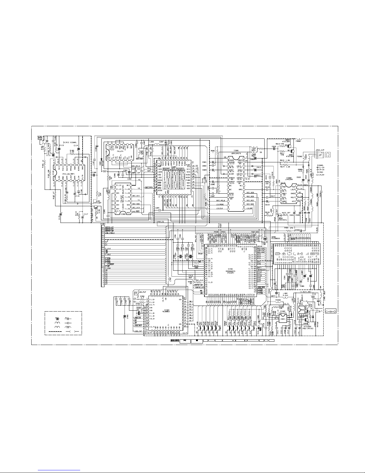
IC
S2-153-410-180 IC,BA3410AF-E2
S2-157-47S-002 IC,HD74LV74
S2-157-41S-003 IC,HD74LV157
S2-163-50S-002 IC,MAS3507D
S2-166-65S-001 IC,MSM66Q573
S2-151-67S-011 IC,MAX1675
87-A21-589-080 IC,R1120N251A-TL
S2-166-08S-001 IC,ML60851C
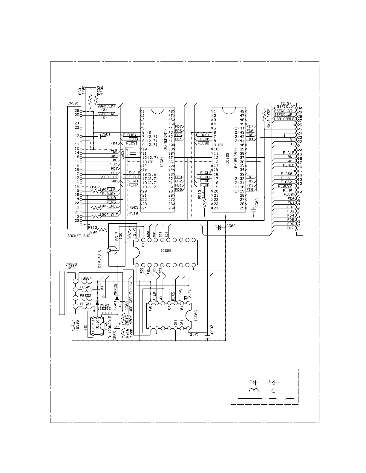
S2-151-28S-001 IC,KM29U128000T
S2-171-12S-002 IC,R1120N331B-TL
S2-157-43S-001 IC,HD74LV32
S2-157-40S-003 IC,HD74LVC245
S2-161-34S-001 IC,UDA1345TS
S2-154-53S-058 IC,LA4534M
TRANSISTOR
S2-461-500-060 C-TR,KTA1504S-Y
S2-482-30S-001 C-FET,SI2305DS
S2-453-260-180 C-TR,KTC3265-Y
S2-451-300-060 C-TR,KTD1304
87-026-334-080 C-TR,DTA143TU
DIODE
S2-550-000-050 D-SCHOTTKY/CHIP MA729
87-017-779-080 C-DIODE,1SS355
MAIN C.B
C111 S8-552-269-210 CAP,TA 22UF-6.3V
C112 S8-552-249-810 CAP,TA 0.22UF-35V
C113 S8-553-359-210 CAP,TA 3.3UF-6.3V
C114 S8-552-269-210 CAP,TA 22UF-6.3V
C115 S8-552-269-210 CAP,TA 22UF-6.3V
C116 S8-552-269-210 CAP,TA 22UF-6.3V
C117 S8-552-269-210 CAP,TA 22UF-6.3V
C206 S8-564-769-110 CAP,TA 47UF-6.3V
C207 S8-564-769-110 CAP,TA 47UF-6.3V
C306 S8-552-259-310 CAP,TA 2.2UF-10V
C307 S8-552-259-310 CAP,TA 2.2UF-10V
C308 S8-552-259-310 CAP,TA 2.2UF-10V
C409 S8-552-269-210 CAP,TA 22UF-6.3V
C412 S8-564-769-110 CAP,TA 47UF-6.3V
C414 S8-564-769-110 CAP,TA 47UF-6.3V
C419 S8-552-269-210 CAP,TA 22UF-6.3V
C420 S8-564-769-110 CAP,TA 47UF-6.3V
C423 S8-564-769-110 CAP,TA 47UF-6.3V
C601 S8-552-269-210 CAP,TA 22UF-6.3V
C603 S8-552-269-210 CAP,TA 22UF-6.3V
C606 S8-552-269-210 CAP,TA 22UF-6.3V
C609 S8-552-269-210 CAP,TA 22UF-6.3V
C612 S8-552-269-210 CAP,TA 22UF-6.3V
C619 S8-552-269-210 CAP,TA 22UF-6.3V
C622 S8-612-211-030 CAP,E 220UF-5,4V
C623 S8-612-211-030 CAP,E 220UF-5,4V
C628 S8-552-269-210 CAP,TA 22UF-6.3V
C631 S8-552-269-210 CAP,TA 22UF-6.3V
C705 S8-564-769-110 CAP,TA 47UF-6.3V
CN401 S1-670-20S-008 BOARD CONN 30P
FB201 S4-453-R30-230 C-COIL,3.3UH
FB401 S4-461-020-100 FERRITE BEAD-CHIP
FB402 S4-461-020-100 FERRITE BEAD-CHIP
FB601 S4-461-020-100 FERRITE BEAD-CHIP
FB602 S4-461-020-100 FERRITE BEAD-CHIP
FB603 S4-461-020-100 FERRITE BEAD-CHIP
FB604 S4-461-020-100 FERRITE BEAD-CHIP
FB605 S4-461-020-100 FERRITE BEAD-CHIP
J201 S5-110-000-510 JACK,HP 3.5-ST BLK
J401 S5-130-000-020 JACK,DC 2.35 BLK
L202 S4-451-000-050 C-COIL,10UH
L203 S4-451-000-050 C-COIL,10UH
L204 S4-451-000-050 C-COIL,10UH
L401 S4-452-200-040 C-COIL,22UH
L402 S4-453-R30-230 C-COIL,3.3UH
L403 S4-453-R30-230 C-COIL,3.3UH
L406 S4-451-000-050 C-COIL,10UH
L605 S4-453-R30-230 C-COIL,3.3UH
L607 S4-451-000-050 C-COIL,10UH
L608 S4-451-000-050 C-COIL,10UH
L609 S4-453-R30-230 C-COIL,3.3UH
L701 S4-451-000-050 C-COIL,10UH
LCD301 S2-730-00S-037 DISPLAY LCD(MMVX100)
MC501 S9-320-000-110 MIC,CON/UNIT
S0 S6-750-300-010 SW,TACT CHIP SKQDABE010(MMVX10
S1 S6-750-300-010 SW,TACT CHIP SKQDABE010(MMVX10
S2 S6-750-300-010 SW,TACT CHIP SKQDABE010(MMVX10
S3 S6-750-300-010 SW,TACT CHIP SKQDABE010(MMVX10
S4 S6-750-300-030 SW,TACT CHIP SKQTLBE010(MMVX10
S5 S6-750-300-030 SW,TACT CHIP SKQTLBE010(MMVX10
S6 S6-750-300-030 SW,TACT CHIP SKQTLBE010(MMVX10
S7 S6-750-300-010 SW,TACT CHIP SKQDABE010(MMVX10
S8 S6-750-300-010 SW,TACT CHIP SKQDABE010(MMVX10
S9 S6-750-300-010 SW,TACT CHIP SKQDABE010(MMVX10
S10 S6-750-300-010 SW,TACT CHIP SKQDABE010(MMVX10
S11 S6-750-300-010 SW,TACT CHIP SKQDABE010(MMVX10
S12 S6-750-300-010 SW,TACT CHIP SKQDABE010(MMVX10
S13 S6-250-120-130 SW,SLIDE CHIP 1C2P(MMVX100)
X401 S3-510-000-190 X’TAL,SEAM14.725M 20PPM(MMVX10
X402 S3-510-000-050 X’TAL,32.768KHZ 20PPM(MMVX100)
X701 S3-510-00S-025 X’TAL(SMD)CSTCW4800MX-4100
SUB C.B
C505 S8-552-269-210 CAP,TA 22UF-6.3V
C506 S8-552-269-210 CAP,TA 22UF-6.3V
C508 S8-552-269-210 CAP,TA 22UF-6.3V
CN402 S1-670-20S-007 BOARD CONN 30P
CN501 S1-670-20S-010 SMART CONN CN015R-3123
CN503 S1-670-20S-023 USB CONN 4P
FB501 S4-461-020-100 FERRITE BEAD-CHIP
FB502 S4-461-020-100 FERRITE BEAD-CHIP
FB503 S4-461-020-100 FERRITE BEAD-CHIP
FB504 S4-461-020-100 FERRITE BEAD-CHIP
FB505 S4-461-020-100 FERRITE BEAD-CHIP