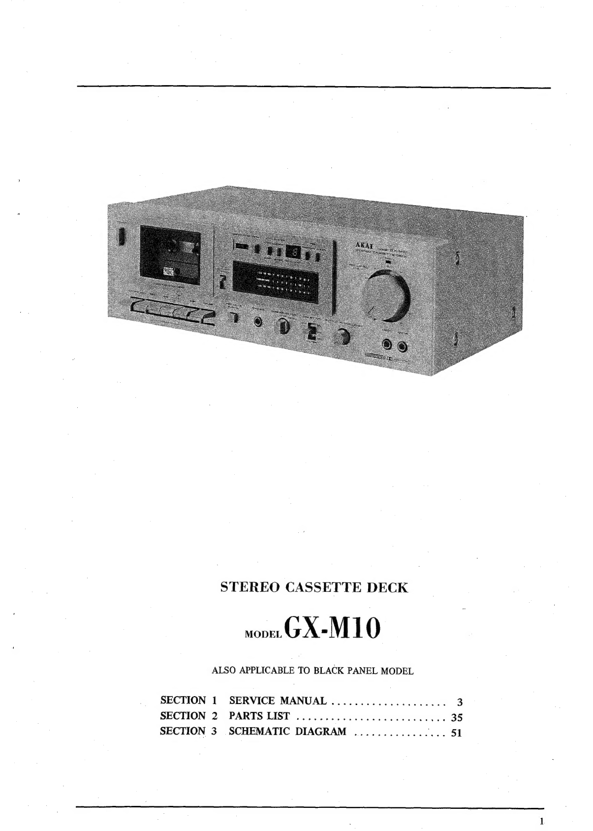
Akai GX-M10 User manual

I
SERVICE
MANUAL
AKAL
pose
etgdtlecds
ery
SJ
Sree
——
==
=
Ih
10008.
ete
|
Cex
=
STEREO
CASSETTE
DECK
MODEL
GX-M!1
Oo

STEREO
CASSETTE
DECK
MODEL
GX-M
1
0
ALSO
APPLICABLE
TO
BLACK
PANEL
MODEL
SECTION
1
SERVICE
MANUAL
....................
3
SECTION
2
PARTS
LIST
............
000s.
esas
ceeee
35
SECTION
3.
SCHEMATIC
DIAGRAM
................
51


SECTION
1
SERVICE
MANUAL
TABLE
OF
CONTENTS
I.
TECHNICAL
DATA...
2.0.2
cece
cece
tenet
e
ee
en
ec
ene
eenes
4
I
DISMANTLING
OF
UNIT
......6
0.
0cceceeeeeesteeeeteeeesees
5
Wil:
-CONTROLS
ccc
sack
Pah
a
tenensaeesd
ats
cal
ce
trata
6
IV.
PRINCIPAL
PARTS
LOCATION
.........55.0+0
00005:
snsehcahanes
7
V.
VOLTAGE
AND
CYCLE
CONVERSION
..........0020000
000s
ava
8
i:
VOLTAGE
CONVERSION
a.s0:5:k4
Okc
voto
toneeoseeatenes
8
A
CVGLE
CONVERSION
cia
yids
Scion
dd
vbe
teh
bame
dn
et
ar
ee
8
VI.
IPSS
CIRCUITRY
OPERATION
EXPLANATION
.........2--0+0
0005
9
VIL
TIMER
START
SWITCH
OPERATION
...........000
00s
ee
seers
17
VIN.
AUTO
STOP
MECHANISM
OPERATION
.........0-.000
0
ee
eres
18
IX,
MECHANISM
ADJUSTMENT
.........0-
00.0
0ee
secu
eeeee
eens
20
X.
HEAD
ADJUSTMENT
..........00000
eee
cere
Lada
eeu
eaies
22
XI.
AMPLIFIER
ADJUSTMENT
.......
Selon’
S
fclasde
ace
aaa
ahecontetonitat
e
_
XII.
DC
RESISTANCE
OF
VARIOUS
HEADS
.......---
00-000
ee
ee
eees
28
XIII.
CLASSIFICATION
OF
VARIOUS
BC
BOARDS
&:
sebas
eeetieeiaws
28
For
basic
adjustments,
measuring
methods,
and
operating
principles,
refer
to
GENERAL
TECHNICAL
MANUAL.
.
:

1.
TECHNICAL
DATA
nn
nn
EEE
EESss
EES
TRACK
SYSTEM
4
track
2
channel
stereo
system
TAPE
Philips
type
cassette
TAPE
SPEED
4.76
cm/s
+
1.5%
(1-7/8
ips.
+
1.5%)
.
HEADS
(2):
Erase
head
x
1
ite
Twin
field
Super
GX
head
x
1
MOTOR
(1):
Electronically
speed
controlled
DC
motor
WOW
&
FLUTTER
i
Less
than
0.04%
WRMS.
0.14%
(DIN
45500)
TAPE
WINDING
TIME
90
sec.
using
a
C-60
cassette
tape
FREQUENCY
RESPONSE
LN
30
to
15,000
Hz
+
3
dB
(-20
VU)
LH
30
to
16,000
Hz
+
3
dB
(20
VU)
CrO,
(SA)
30
to
16,500
Hz
+
3
dB
(-20
VU)
30
to
8,000
Hz
+
3
dB
(0
VU)
Metal
30
to
19,000
Hz
+
3
dB
(-20
VU)
30
to
12,000
Hz
+
3
dB
(0
VU)
SIGNAL
TO
NOISE
RATIO
LN
better
than
58
dB
LH
better
than
59
dB
CrO,(SA)
better
than
60
dB
Metal
better
than
61
dB
(Measured
via
tape
with
peak
recording
level)
Dolby
NR
switch
ON:
Improves
up
to
10
dB
above
5
kHz
HARMONIC
DISTORTION
CHANNEL
SEPARATION
LN
less
than
0.8%
LH
less
than
0.8%
CrO,
(SA)
less
than
0.7%
Metal
less
than
0.6%
27
dB
at
1,000
Hz
©
ee
ee
CROSS
TALK
60
dB
at
1,000
Hz
INPUT
MIC:
0.3
mV
(Input
impedance
5.0
kohms)
Required
microphone
impedance:
600
ohms
Line:
70
mV
(Input
impedance
47
kohms)
OUTPUT
Line:
410
mV
at
0
VU
;
Required
load
impedance:
more
than
20
kohms
Phone:
100
mV/8
ohms
at
0
VU
DIN
Input:
2.0
mV
(Input
impedance
10
kohms)
Output:
410
mV
Required
load
impedance:
more
than
20
kohms
DIMENSIONS
440(W)
x
143(H)
x
250(D)
mm_=
(17.3
x
5.6
x
9.8")
WEIGHT
6.0
kg
(13.2
lbs)
POWER
CONSUMPTION
POWER
REQUIREMENTS
7
12
W
100V,
50/60
Hz
for
Japan
120V,
60
Hz
for
U.S.A.
&
Canada
220V,
50
Hz
for
European
countries
except
U.K.
240V,
50
Hz
for
U.K.
&
Australia
110/120/220/240V
switchable,
50/60
Hz
for
the
other
countries
*
For
improvement
purposes,
specifications
and
design
are
subject
to
change
without
notice.
*
“Dolby”
and
the
Double
D
symbol
are
trademarks
of
Dolby
Laboratories.
(Manufactured
under
license
from
Dolby
Laboratories).

DISMANTLING
OF
UNIT
In
case
of
trouble,
etc.
necessitating
dismantling,
please
dismantle
in
the
order
shown
in
the
photographs.
Reassemble
in
reverse
order.
SCREWS
SCREWS
FRONT
PANEL
SCREWS
UPEER
COVER
BACK
BOARD
SCREWS
CONTROL
KNOBS
LID
PANEL
Pult
toward
you
both
lower-ends
of
folder.

i.
CONTROLS
No
10.
11.
12.
POWER
SWITCH
CASSETTE
RECEPTACLE
TIMER
START
SWITCH
INDEX
COUNTER
AND
RESET
BUTTON
AUTO
SYSTEM
SWITCH
|
MEMORY/IPSS
SWITCH
PROGRAM
DISPLAY
.
IPSS
PROGRAM
SWITCH
CLEAR
SWITCH
FL
DISPLAY
BAR
METER
RECORDING
INDICATOR
LAMP
LEFT
—*}-RIGHT
RECORDING
LEVEL
CONTROLS
13.
14.
15.
16.
17.
18.
19.
20.
21.
22.
23.
Fig.
1
Controls
MICROPHONE
JACKS
OUTPUT/PHONES
LEVEL
CONTROL
DOLBY
NR
SWITCH
AND
FILTER
TAPE
SELECTOR
HEADPHONE
JACK
REC
MUTE
OPERATING
KEYS
LINE
OUTPUT
JACKS
DIN
JACK
(The
JPN,
USA
models
do
not
have
this
facility)
LINE
INPUT
JACKS
INPUT
SELECTOR
SWITCH
(The
JPN,
USA
models
do
not
have
this
facility)

iv.
PRINCIPAL
PARTS
LOCATION
_REC/PB
HEAD
H9O!
PR4-7
POWER
SWITCH
WIND.
SWITCH
SWE
SW903:
=:
os
PROGRAM_LED
;
“SWITCH
SWI.
RC
BOARD
CE-5206B
UsTIMER
“START:
=~:
[oss5:s
MEMORY/IPSS:
|
ss
PROGRAM.
SWITCH
SWITCH
>
fo
Se
SWITCH
SW2
vote
SW4
CLEAR
SWITCH
sw3
LED
P.C_
BOARD
CE-5201B
MUTE
SWITCH
Sw902
BAR
METER
INDI
ERASE
HEAD
H902
E-921
PHONES
JACK
J3
DOLBY
NR
AND
FILTER
REC
LEVEL.
SWITCH
SW3
CONTROLS
VR!
REC
MUTE
SWITCH
TAPE
SELECTOR
sw5 Sw4
OUTPUT
LEVEL
CONTROL
VR!
L
R
Ld
MIC
JACKS
Fig.2
Front
View
VOLTAGE
SELECTOR
vsi
POWER
SUPPLY
P.C
BOARD
CE-5202
POWER
TRANSFOMER
CET-
2!
PRE
AMP
_P.C
BOARD
CE-S5201A
POWER
SWITCH
MOTOR
sw!
M901
MMI-6A2LK
SYS.CON
RC
BOARD
CE-5206A
Fig.3
Top
View

V.
VOLTAGE
AND
CYCLE
CONVERSION
POWER
SUPPLY
RC
BOARD
CE-5202
POWER
CORD
SHORT
PIN
Fig.
4
Voltage
Conversion
(U/T
Model)
1.
VOLTAGE
CONVERSION
2.
Loosen
holding
screws
and
remove
upper
cover
Models
for
Canada,
Europe,
USA,
UK,
Australia
and and
back
board.
;
Japan
are
not
equipped
with
this
facility.
3.
Remove
short
pin
plug
from
present
holes
and
Each
machine
is
preset
at
the
factory
according
to
replace
in
correct
holes.
Follow
the
markings
destination,
but
some
machines
can
be
set
to
110V,
explicitly.
120V,
220V
or
240V
as
required.
If
voltage
change
is
necessary,
this
can
be
accom-
plished
as
follows:
2.
CYCLE
CONVERSION
1.
Disconnect
power
cord.
With
DC
motor,
cycle
conversion
is
not
necessary.

Vil.
IPSS
CIRCUITRY
OPERATION
EXPLANATION
¥
©
CLEAR
PROGRAM
©
\
LINE
OUT
De
(LEFT)
BLANKING
DISPLAY
COMPARATOR
REFERENCE
VOLTAGE
LINE
OUT
2
(RIGHT)
he
LINE
AMP
-
TAPE
COUNTER
&
(000)
ONE
SHOT
PULSE
:
GENERATOR
STOP
|
peu
ON
OorF
|
IPSS
OMEMORY
ae
OOFF
AUTO
SYSTEM
1.
IPSS
(Instant
Program
Searching
System)
is
the
pro-
graming
in
advance
of
the
song
or
songs
(up
to
9
from
the
present
position
on
the
tape)
you
want
to
listen
to.
When
the
FF
or
RWD
and
PLAY
keys
are
depressed
simultaneously,
the
no
signal
portion
between
songs
is
detected
by
the
REC/PB
head
and
the
number
of
these
is
counted
down
according
to
the
programmed
number
of
songs.
As
it
goes
from
1
to
0,
the
FF
or
RWD
key
is
released
and
it
enters
the
Play
mode.
2.
CIRCUITRY
DETECTING
THE
NO
SIGNAL
PORTION
(Refer
to
Figs.
6,
7,
&
8)
When
the
FF
or
RWD
and
PLAY
keys
are
depressed
simultaneously,
the
REC/PB
contacts
the
tape
and
the
signal
on
the
tape
is
picked
up
by
REC/PB
head.
The
head
is
about
1.7
mm
lower
than
it
would
be
in
the
playback
mode.
The
picked
up
signal
is
added
to
input
IC1-1
@
in
the
Limiter
Amp.,
it
is
amplified,
detected
by
D2
and
added
as
TR1’s
base
bias.
TR1
is
ON
and
IC1-2
©
is
practically
earth
potential.
The
standard
voltage
of
the
Comparator
(IC1-2)
is
1/2
Vcc
(about
6V)
so
the
output
@
becomes
Vcc
(about
12V).
When
a
no
signal
portion
is
reached,
base
bias
is
not’
added
to
TRI
and
it is
turned
OFF.
C3
charges
and
IC1-2
@
becomes
Low
Level
at
the
point
that
|,
[i
F.F./RWD
KEYS
REC
KEY
REC
MUTE
BUTTON
Fig.5
IPSS/MEMORY
SYSTEMS
BLOCK
DIAGRAM.
NOTE
1.
SWITCHS
ENCLOSED
BY
[___]
ARE
MANUAL.
2.
&
1S
A
SWITCH
CIRCUIT.
LEFT
AND
RIGHT
ARE
CONNECTED
ONLY
WHEN
A
COMMAND
IS
INPUT
4.
IC1-2
©’s
potential
exceeds
the
standard
voltage
(1/2
Vcc)
in
the
comparator.
As
a
result,
charging
current
flows
into
C5
and
a
trigger
pulse
is
generated
at
the
cathode
side
of
D14.
IC2
counts
down
by
this
pulse’s
falling
portion.
C2
and
RS
are
to
compensate
for
the
high
frequency
level
drop
caused
by
the
head
not
touching
the
tape
perfectly.
When
there
is
noise
in
the
portion
between
songs
on
the
tape,
there
is
more
than
one
trigger
pulse
generated
in
the
portion
making
miscounting
a
probability.
C5’s
charged
and
discharged
electricity
are
used
to
prevent
this
occuring.
C5
is
charged
through
D3
and
R56
while
IC1-2
@
is
at
Low
Level
(no
signal
portion
between
the
songs
on
the
tape)
and
both
terminal’s
voltage
difference
is
almost
Vcc
(+12V).
When
the
no
signal
portion
is
over
IC1-2
@
becomes
High
Level
and
because
it
is
piled
on
to
the
potential
charged
to
C5,
D14’s
cathode
side’s
potential
becomes
higher
than
+B’s
(+12V)
potential.
Then
C5
will
discharge
through
R14
until
both
terminal’s
potentials
are
equal.
Until
C5
discharged
down
to
a
certain
level
even
if
IC1-2
@
becomes
Low
Level,
only
a
small
trigger
pulse
is
created
in
the
D14
cathode
side
and
does
not
reach
the
IC2’s
DOWN
COUNT
operation
level.
Therefore
the
programme
counter
does
not
count.
rn
a
ee
ne
ems
aaa]
SERGE
9

C1
TRt
NJM4558D
28C945L(PH(Q)
IS2473VE
03
i
4
@
WOK
R
100td}
R56
4,7K
02
R4
IS2473VE
1
|
Lech
INO—”——+
(7)
ut
Rch
INO—w—-+1
2
=
a
©
i
I
§
<
os
6)
ae
pees
Bla
ded
&
m2
wo
m
a
1p
PEO
:
a
EP
eee:
—t
FL)
=
soelsi
ti
a&
©
(10)
nu
+17V
tIqo
)
KON
Poul
ae
|
eOw
(3)
Prerrreae
ga
gaa
a
a
@10
I
I
!
sw90l
'
w
WIND
i.
Fa
sWw903
28c945L(P)(Q)
!
23¥
|
|
i
ies
H
O
18247
3VE
ae
!
=
i
¥
i
S
g
tf
i
S
.
lye
3S
OO
OF
2
t
°
2Sa733(
PQ)
sw5-2t—4
H
i
—=ON
|
7%
ONE
SHOT
PULSE
GENERATOR
(REC
MUTE]
EC
MOT
I
I
IPSS
PROGRAM
TRS
2SC945L(P}(Q)
+17V0
+27VO0
IS2473VE
x2
SL30]
O520PLT1
r
Ise
1s
fe
1g
“7,
MONOSTABLE
ASTABLE
MULTIVIBRATOR
MULTIVIBRATOR
Fig.6
IPSS/MEMORY
SYSTEMS
SCHEMATIC
DIAGRAM
10

MUSIC-I_
MUSIC
-2
(a)
I¢
1-1
@)
tb)
IC
1-1
o—_—
st
(atc
1-2
6)
1/2Vec
enc
i-2
@
{f)
DI4
CATHODE
DOWN
COUNT
Fig.
7
>
BLANK
NOSE
|
MusIC
|
4
he
1
MUSIC
“@ici-2
@
}
|
;
.
|
|
|
ie
C5~RI4
DISCHARGE
ae
CHARACTERISTICALY
DOWN
COUNT
OPERATION
LEVEL
OF
Ic2
{b)
DI4.
CATHODE
Fig.
8
When
there
is
noise
in
the
portion
between
songs
on
the
tape
11

3.
CIRCUIT
CONSTRUCTION
OF
IC2
MSM
5953RS
Function
BCD
UP/DOWN
COUNTER/7
SEGMENT
DECODER/DRIVER
Construction
CMOS
IC
1)
Block
Diagram
uP
IN
C1)
1
SCHMIDT
CONTROL
j
1
I
I
|
{
I
|
I
'
!
i
u/D
()
DOWN
OUT
DOWN
IN
r
2)
Terminals
and
their
functions
1.
2
3.
UP
IN:
Counts
up
(+1)
using
the
raised
portion
_FL
of
the
pulse.
DOWN
IN:
Counts
down
(—1)
using
the
falling
portion
+J
of
the
pulse.
Does
not
count
at
0.
DOWN
OUT:
Outputs
when
there
is
DOWN
IN
input.
,
When
a
condenser
is
attached
between
this
and
GND,
after
input
enters
the
DOWN
IN
terminal,
the
delayed
time
can
be
adjusted
up
—
until
the
counter
counts
down.
.
U/D
(UP/DOWN):
There
is
input
to
the
DOWN
IN
terminal
but
counts
down
only
when
this
‘terminal
is
Low
Level.
f
(3)
COUNTER
I
\
I
(2)
SCHMIDT
|
I
|
BCD
7
SEGMENT
DECODER
1a)
~
(6)
BORROW
OUT
SEGMENT
DRIVER
OUT
ant
eaerFr
Aa
-----©®OG0O@---
Fig.9
MSM5953RS
.
RBI
(Ripple
Blanking
Input):
When
put
to
Low
Level
the
counter
display
(LED)
is
extin-
guished.
BORROW
OUT:
There
is
momentary
output
when
there
is
DOWN
input
after
the
counter
goes
from
1
to
Qor
from
0.
.
RESET:
When
put
to
Low
Level
the
counter
is
reset
to
0.
to
15
SEGMENT
OUT:
Connects
the
Anode
Common
7
Segment
LED.
Light
up
when
put
to
Low
Level.

3)
Function
Table
COUNT
CONDITION
BORROW
OUT
X
=
Doesn’t
matter
Chart-2
RESET
uD
|
DOWNIN
|
UPIN
|
COUNT
CONDITION
|
COUNT
H
#H
xX
a
xX
a
NO
.
|
a
X
x
UPCOUNT(#1)
|
art
ee
=F
an
eee
ae?
ae.
X
|_NO
|
H
L L
a
X
UPCOUNTGH)
|
H
|
OL
=e
H
1
to9
|
DOWN
COUNT
(-1)
a
a
ee
ae
H
0
No.
[
4
ae
ee
X
X
CLEAR
(0)
X
=
Doesn’t
matter
Chart-1
13

+8
REwso!
~1C
2D
UP
IN
OFF
REC
MUTE
SW
Fig.
10
Oscillation
Stopped
.
+8
+B
*swao!
IC
2)
uP
IN
=
ON
REC
MUTE
SW
cis
ip:
R48
!
2
~=>
UP
COUNT
(b)
O
(a)
a
ei
Fig.
11
Oscillation
14

4.
OSCILLATOR
CIRCUITRY
FOR
REC
TIME
COUNT
(Refer
to
Figs.
10
and
11)
This
circuit
is
to
indicate
the
Rec
Mute
Time
Count
in
Program
LEDs
-and
to
add
one
second
interval
pulses
to
the
UP
IN
terminal
of
IC2.
When
the
Rec
Mute
button
is
not
depressed,
IC3a’s
input
terminal
@3
is
“L”
and
IC3b’s
output
terminal
@
is
“L”.
C13
has
been
discharged
as
in
Fig.
10
and
1C3a’s
input
terminal
@
is
changed
to
“H”
by
this
potential.
At
this
point,
when
the
REC
MUTE
switch
is
depressed,
IC3a’s
@3
changes
to
“H”
IC3a’s
output
terminal
@D
to
“L”
and
IC3b’s
@
to
“H’”.
As
IC3’s
@
has
become
“L”,
C13
discharged
through
R44.
During
this
discharging
period
(time
constants
of
C13
and
R44)
IC3’s
@
becomes
“H”
due
to
the
voltage
drop
at
both
terminals
of
R44.
Once
C13
has
finished
discharging,
there
is
no
current
flowing
in
R44
and
the
voltage
drop
is
0
so
IC3a’s
@
changes
to
“L”.
As
a
result
IC3a’s
@)
becomes
“H”,
IC3b’s
GO
“L”
and
this
time
the
charging
current
flows
from
IC3a’s
@)
throught
R44
to
C13.
During
this
charging
period
(Fixed
time
constants
of
R44
and
C36)
IC3a’s
@)
becomes
“L”.
After
C36
has
been
charged,
due
to
this
potential,
IC3a’s
@,
changes
to
“H”,
@
to
“L”
and
IC3b’s
@
to
‘“H’’.
The
above
operation
is
repeated
and
a
1
Hz
square
wave
appears
at
IC3b’s
output
terminal
®
.
MONOSTABLE
MULTIVIBRATOR
OPERATION
(Refer
to
Fig.
6)
A
plunger
is
activated
by
IC2’s
output
©
to
release
the
FF
or
RWD
key
in
the
IPSS
mode.
However
in
IC2’s
output
there
is
a
pulse
width
which
is
too
narrow
to
drive
the
transistor
directly
so
the
pulse
width
is
enlarged
by
a
Monostable
vibrator,
the
transistor
drive
is
corrected
and
then
the
plunger
is
activated.
.
ONE
SHOT
PULSE
GENERATOR
(Refer
to
Fig.
6)
This
circuit
resets
the
counter
for
an
instant
when
the
REC
key
has
been
depressed
while
the
REC
Mute
switch
is
being
depressed.
When
the
REC
key
has
been
depressed
after
the
REC
Mute
key,
if
TR14
has
not
been
attached,
TR4
turns
off
and
the
IC2
counter
does
not
reset.
If
the
counter.
is
counting
down
numbers
with
the
program
switch
these
numbers
will.
be
increased
by
the
time
taken
to
depress
the
REC
Mute
switch.
To
prevent
this,
when
the
REC
switch
is
put
on
TR14
is
put
on
simultane-
ously
for
a
certain
period
(the
difference
between
C70’s
and
C71’s
charging
periods)
of
time
only.
When
TR14
is
turned
on
TR4
turns
on
and
the
counter
is
reset.
Therefore
the
REC
MUTE
TIME
indication
begins
from
0.
15

CAM
LEVER(A)
PLAY,RWD
KEY
.
DESCRIPTION
OF
KEYBOARD
OPERATION
(Refer
to
Fig.
12)
With
IPSS
and
MEMORY
operation
the
PLUNGER
is
activated
and
pulls
the
KEYBOARD
CAM
back.
Only
the
FF
or
the
RWD
keys
are
released
and
the
deck
is
put
in
the
playback
mode
by
the
combination
of
the
KEYBOARD
CAM,
the
PLAY
CAM
and
the
CAM
LEVERS
(A)
and
(B).
The
PLAY
CAM
and
the
KEYBOARD
CAM
are
fixed
by
slotting
CAM
LEVERS
(A)
and
(B)
into
section
A
of
the
KEYBOARD
CAM.
(Refer
to
Fig.
12a.)
Now
in
the
IPSS
mode,
when
the
RWD
and
PLAY
keys
are
depressed
simultaneously,
the
RWD
key
attaches
to
the_J
L
section
of
the
KEYBOARD
CAM
and
the
PLAY
key
to
the
[
L
section
of
the
PLAY
CAM.
.
CAM
LEVER
(B)
which
is
being
held
up
with
CAM
LEVER
(A)
by
the
RWD
key
also
moves
in
the
_
direction
of
the
arrow.
(Fig.
12a,
b)
CAM
LEVER(B)
CAM
LEVER(A)
Fig.
12
CAM
LEVERS
(A)
and
(B)
separate
from
the
section
A
which
is
fixing
the
KEYBOARD
CAM
and
the
PLAY
CAM
so
even
if
the
KEYBOARD
CAM
is
pulled
backwards,
PLAY
CAM
remains
attached
to
the
PLAY
key
and
does
not
move
backwards.
Therefore
even
when
the
PLUNGER
pulls
the
KEYBOARD
CAM
backwards
because
of
the
IPSS
and
MEMORY
operation,
the
PLAY
CAM
does
not
move
back
with
the
result
that
only
the
RWD
key
is
released
and
the
deck
goes
in
to
the
play
mode.
(Fig.
12c)
This
will
be
the
same
when
the
FF
key
is
depressed
simultaneously
with
the
PLAY
key.
After
the
FF
or
RWD
and
PLAY
keys
have
been
depressed
simultaneously,
when
the
STOP
key
is
depressed
once
only
the
FF
or
RWD
key
will
be
released
so
to
release
the
PLAY
key
the
STOP
key
must
be
depressed
one
more
time.
This
is
due
to
the
operation
outlined
above.
a

VIL.
THMER
START
SWITCH
OPERATION
WORM
PULLY
Fig.
13
The
TIMER
START
SWITCH
is
designed
to
put
the
deck
in
the
REC
or
PLAY
modes
by
releasing
the
PAUSE
key
automatically
(the
PAUSE,
REC
and
PLAY
keys
have
already
been
depressed)
when
the
power
is
turned
on
by
the
timer.
In
the
PAUSE
mode,
the
PAUSE
SLIDE
is
lifted
up
and
fixed
by
attaching
the
LOCK
PIN
to
the
LOCK
CAM
so
to
release
the
PAUSE
mode
all
you
have
to
do
is
to
detach
the
LOCK
PIN
from
the
LOCK
CAM.
When
put
into
the
PAUSE
mode,
the
LOCK
PIN
is
attached
to
the
LOCK
CAM
and
the
PAUSE
SLIDE
is
locked.
When
the
TIMER
START
SWITCH
is
put
on
—
TIMER
SLIDE
(A)
moves
upwards
and
as
a
result,
TIMER
SLIDE
(B)
moves
upwards
to
the
inside
in
the
direction
of
the
arrow
and
downwards
to
the
outside.
See
Fig.
13b.
If
the
power
switch
is
turned
on
here,
the
WORM
-
PULLEY
and
the
WORM
GEAR
revolve.
The
pin
on
the
WORM
GEAR
CAP
moves
in
the
direction
of
the
arrow
TIMER
SLIDE
(B)
is
pushed
down
so
the
LOCK
CAM
is
pushed
upwards
by
this
section.
Then
the
LOCK
PIN
is
detached,
the
PAUSE
SLIDE
lowers
and
the
PAUSE
key
is
released.
The
TIMER
START
SWITCH
is
also
released
because
TIMER
SLIDE
(A)
is
pushed
down
by
TIMER
SLIDE
(B).
17

VII.
AUTO
STOP
MECHANISM
OPERATION
~—
RELEASE
LEVER
AS
ARM
SPRING
f
oan
AS
LEVER
Lig
aia
PULLY
Fig.
14
WORM
GEAR
(a)
(b)
(c)
AS
ARM
SPRING
Fig.
16

a
AUTO
STOP
puts
the
deck
into
the
STOP
mode
by
releasing
the
keys
when
the
end
of
the
tape
is
reached
in
the
PLAY,
FF,
RWD
REC/PB
modes.
1.
HOW
EACH
PART
OPERATES
—__
a.
CLUTCH
PLATE
(B)
(Fig.
14)
©
There
is
felt
attached
to
this
and
friction
force
is
generated
(Shown
by
the
arrow)
and
it
seems
as
if
it
is
pushing
the
AS
ARM
outwards.
b.
AS
LEVER
(Figs.
14,
16)
The
pin
attached
to
the
rear
of
the
AS
LEVER
enters
the
groove
of
the
WORM
GEAR.
It
touches
against
thet
section
a
as
the
WORM
GEAR
revolves
and
moves
to
the
left
or
right
or
is
pushed
down
by
ct
section
B.
c.
RELEASE
LEVER
(Fig.
14)
Adds
the
same
friction
force
to
the
AS
ARM
by
pulling
down
the
AS
ARM
Spring
in
the
pause
mode
as
when
the
reel
revolves.
-
2.
When
put
into
the
PLAY
(FF,
RWD)
mode
the
fly-
wheel
revolves
and
the
WORM
pulley
and
WORM
gear
revolves.
The
reel
revolves
and
the
CLUTCH
PLATE
goes
to
push
the
AS
ARM
outwards
with
the
friction
force
so
the
pin
at
the
rear
of
the
AS
LEVER
‘receives
this
force
to
the
left
then
it
contacts
the
ridged
sectionc!
4A
of
the
WORM
GEAR
and
move
to
the
left
and
right.
At
the
end
of
the
tape,
the
reel
stops
revolving
so
the
friction
disappears.
In
the
PLAY
(FF,
RWD)
mode
the
RELEASE
LEVER
drops
so
friction
is
not
added
to
the
AS
ARM
from
the
AS
ARM
SPRING.
The
Worm
Lever
continues
to
revolve
and
the
AS
LEVER
pin
is
taken
up
to
the
top
of
the
ridged
C4
section
where
it
then
stops.
It
is
then
pushed
down
by
the
WORM
GEAR
section
Bl,
and
pushes
down
the
AS
SLIDE
with
the
AS
LEVER
and
releases
the
PLAY
(FF,
RWD)
keys.
When
the
PAUSE
key
is
depressed
from
the
PLAY
mode
the
reel
stops
revolving
and
the
force
from
the
CLUTCH
PLATE
tothe
AS
ARM
stops.
However
the
PAUSE
SLIDE
moves
upwards
and
pushes
up
the
RELEASE
LEVER
which
had
been
held
down
so
the
same
force
is
applied
as
to
the
AS
ARM
by
the
AS
ARM
SPRING
so
AUTO
STOP
does
not
operate.
Other manuals for GX-M10
1
Table of contents
Other Akai Cassette Player manuals