manuals.online logo
Brands
  1. Home
  2. •
  3. Brands
  4. •
  5. Allview
  6. •
  7. Telephone
  8. •
  9. Allview X1 SOUL User manual

Allview X1 SOUL User manual

Service Manual
X1 Soul
Page 1 of 21
Contents
1. OUTLINE................................................................................................................3
1.1. Mobile Introduction..................................................................................................................................3
1.2. Motherboard Components Distribution.................................................................................................5
2. SIGNAL FLOW AND FAULT ANALYSIS.............................................................5
2.1. RF Part.......................................................................................................................................................5
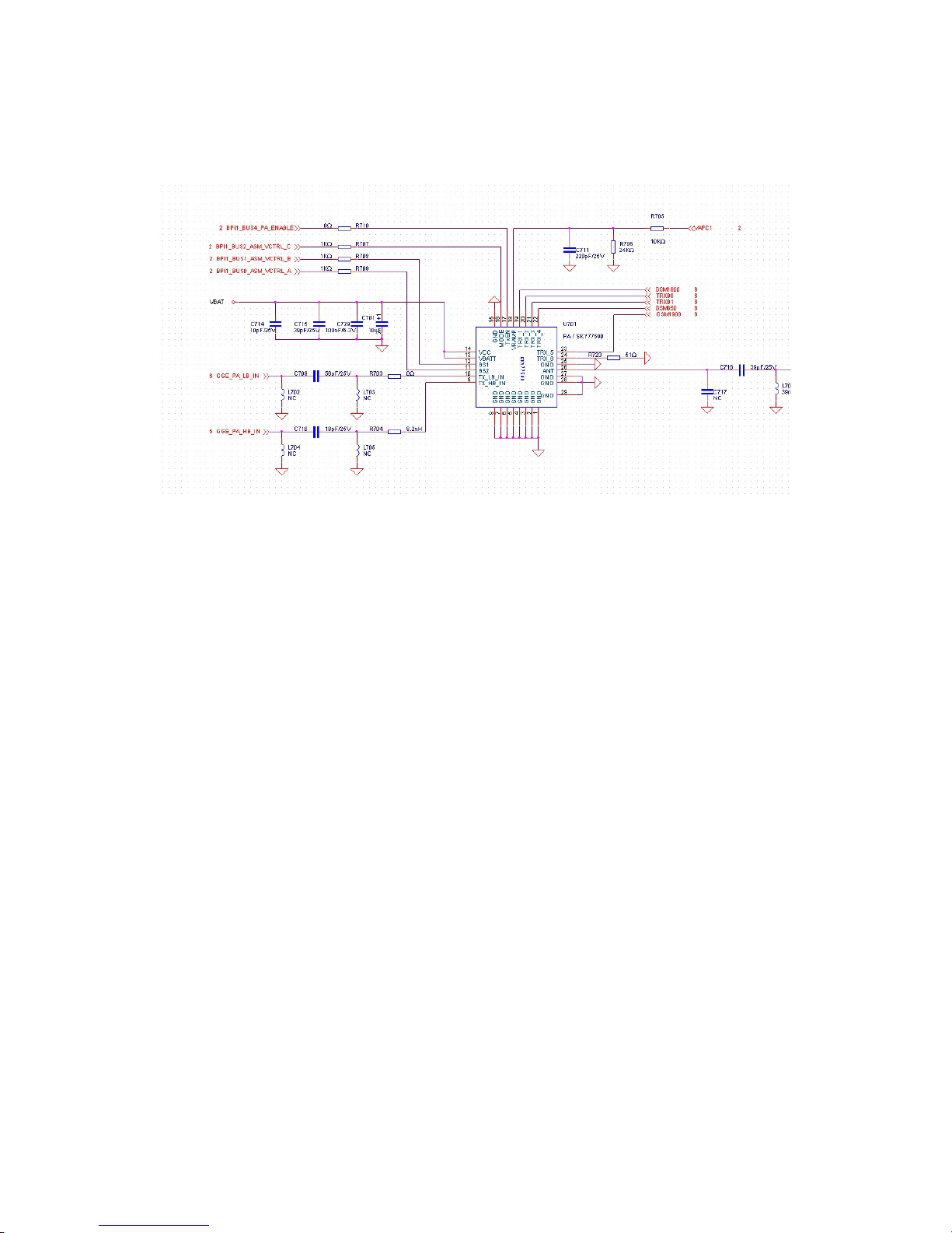
2.1.1. Block Diagram of the RF Section.......................................................................................................5
2.1.2. Signal flow of the RF Transmitting Part.............................................................................................6
2.1.2.1. Transmitting Path...............................................................................................................................6
2.1.2. Signal Flow of the RF Receiving Part................................................................................................7
2.1.3.1. Receiving Path Components...........................................................................................................7
2.2. Baseband part..........................................................................................................................................10
2.2.1 Block diagram of the Baseband part.....................................................................................................10
2.2.2 Power Management...............................................................................................................................11
2.2.3 Audio Section........................................................................................................................................12
2.2.3.1 Audio Codec Circuit.....................................................................................................................12
2.2.3.2 MIC& Receiver Loop...................................................................................................................13
2.2.3.3 Headset Loop................................................................................................................................13
2.2.4 Baseband Fault issues...........................................................................................................................14
2.2.4.1 Analysis of the keyboard fault......................................................................................................15
2.2.4.2 Analysis of Display module circuit..............................................................................................15
2.2.4.3 FM Module...................................................................................................................................16
2.2.4.4 Camera Module............................................................................................................................16
2.2.4.5 IO Interface...................................................................................................................................17
2.2.4.6 SIM Card Circuit..........................................................................................................................17
2.2.4.7 BT/WIFI/GPS Circuit...................................................................................................................18
2.2.4.8 G-sensor Circuit............................................................................................................................18
2.2.4.9 M-sensor Circuit.......................................................................................................................18
2.2.4.10 Gyroscope Circuit....................................................................................................................19
Page 2 of 21
1. Outline
1.1. Mobile Introduction
Product Hardware Definition
Base Chip Set BB MT6589WTK
PMIC MT6320
Transceiver MT6167
Camera DSP/MMP NA
RFPA SKY77590
FM MT6628
BT MT6628
Audio
CODEC&PA
YD165C
Memory Samsung KMI2U000MA-B800
TP IC GT915
Peripheral
Configuration
LCD 5.0"
Backlight driver LM3630
CAMERA 13million pixel
Memory card NA
Antenna monopole
Basic
Performance
Indicators
Leakage current ≤ 90uA
Standby current ≤ 7mA
Call current as
maximum power
TBD
Board-level power GSM 32.5dBm
DCS 29.5dbm
Board-level receiver
sensitivity
GSM -108dbm
DCS -109dbm
TRP GSM 27dbm
DCS 25dbm
Band1 23dbm
Band8 22dbm
TIS GSM -103dbm
DCS -105dbm
Band1 -104dbm
Page 3 of 21
System Block Diagram
Page 4 of 21
CPU
MT6589
PMIC
MT6320
BATTRY
CAMERA
FM 、BT 、
WiFi 、GP
S
LCD&CTP
KEYPAD
MEMORY
MT6167
SKY77590
YD165 SPK
HP
REC
single SIM
CARD
MIC
1.2. Motherboard Components Distribution
2. Signal Flow and Fault Analysis
2.1. RF Part
2.1.1. Block Diagram of the RF Section
RF Block Diagram
Page 5 of 21
A
N
T
PA &
Ant
Switch
SKY7
7590
Transceiver
MT6167
CPU
MT658
9
GG
G
2.1.2.Signal flow of the RF Transmitting Part
2.1.2.1. Transmitting Path
Maintenance Flow Chart of the Transmitting Issue:
Page 6 of 21
2.1.2. Signal Flow of the RF Receiving Part
2.1.3.1. Receiving Path Components
Receiving path is shown in the following figure:
Page 7 of 21
(NO launch )Connect the PC and the phone with maintenance line,
then making the phone into the RF state with META software
Check Transceiver to
see if IQ signals exist.
`
Check the PA output to
see if there is RF signal
in the path.
Y
Check CPU
N
Check RF coaxial
switch or matching
network.
Y
Check the
Transceiver to see if
there is RF signal
output.
N
VBAT,PA_EN,BA
NDSW_DCS,VAP
C whether OK?
Replace PA
Y
Check CPU
Y
Check Transceiver if
LE 、SCLK/SDAT 、RF
VCOEN 、VCXOEN
have the correct signal.
N
N
N
N
Y
Replace Transceiver
Maintenance flow chart of the receiving Issues:
Page 8 of 21
Page 9 of 21
No receiving
Start the META software to connect the PC and the phone ,making the phone into the
receiving state. Signal generator is also adjusted to the correspond CH. And signal lines
connected to the phone.
Coaxial switch on 。
Transceiver has
IQ?
Check CPU Y
Transceiver has
received signal?
Number ?
N
Transceiver SDATA 、
SCLK 、LE 、CXOE
N are correct ?
Y
Check CPU
N
Whether the
voltage of the
transceiver is
normal? Whether
26MHZ is
normal?
Normal ?
Y
Check the
corresponding
power supply and
26MHZ resulting
circuit
N
Replace transceiver
Y
PA has
received
signal?
N
Check to see if there has
signal in the matching
circuit between PA and
ANT
N
Check to see if there
has signal in the
matching circuit
between PA and
transceiver
Y
2.2. Baseband part
2.2.1 Block diagram of the Baseband part
Page 10 of 21
CPU
MT6589
PMIC
MT6320
BATTRY
CAMERA
FM 、BT 、
WiFi 、GP
S
LCD&CTP
KEYPAD
MEMORY
MT6167
SKY77590
YD165 SPK
HP
REC
SINGLE
SIM CARD
MIC
2.2.2 Power Management
The power management module is PMU IC:MT6320.
2.2.2.1 Mobile power supply system
DC-DC:
LDO:
Page 11 of 21
2.2.3 Audio Section
2.2.3.1 Audio Codec Circuit
This phone applies YD165 which is a class D and non-crack noise YAMAHA amplifier to drive speaker.
Block diagram of the audio system is as below:
Page 12 of 21
2.2.3.2 MIC& Receiver Loop
MIC Audio path is shown below :MIC must have a bias voltage in order to operate normally——
2.0±0.1V. When MIC is in good condition but loop MIC has no echo, then you need to check the basic
bias voltage signal of the MICBIASP and MICBIASSP, the language signals of the RECEIVER and MIC
also need to be checked.
Receiver loop is simple. The output of BB drive Receiver directly through Filter and ESD protected
network, as shown below:
2.2.3.3 Headset Loop
Headset loop includes two signals: Headset speaker and MIC ,If the headset fitting were in good
condition, when the headset plug in, it appears abnormal, such as: The Headset speaker has no sound、the
Page 13 of 21
MIC is invalid. All this need to check the access conditions of the circuit above.
2.2.4 Baseband Fault issues
Maintenance process of the download failure Issues:
Page 14 of 21
2.2.4.1 Analysis of the keyboard fault
This handset has 3 side keys. All the keyboard circuits use the scanning method to detect
except the power button .When a button is pressed the scanning signal will be triggered, then
the corresponding row and column will be detected. The function of the key can be identified
according to software definition.
Page 15 of 21
Download Fail
Check to see if it is caused by other
factors such as: configuration, download
cable, power supply, software and PC
Exclude the reason of
download failure
caused by other factors
Yes
Check to see if the serial ports between
pc and cell phone is smooth
Check if the system
connector is poor
soldered or damaged.
NO
NO
Check the resistance,
capacitance and the
EDC devices between
the system connector
and the CPU.
NO
Connect the download cable then
observe the Ammeter to see if it
shows high current (The normal
current generally about 30mA )
Yes Quickly disconnect the
connection, and gently
touch the chip to see if it is
hot. If not, then focus point
using the multi-meter to
measure the short circuit.
Yes
Check the power manager and open the
LDO to see if the voltage supply is
normal and whether there is power
supply circuit open.
Little or no current
Check VCORE 、VDD 、VADD 、VTCXO 、
VRTC 、VMEM 、Measure the clock signal
of 26MHZ 、32KHZ.
Current normal but download fail
Check CPU and NAND FLASH 、SDRAM
to see if they are OK and the LDO is normal.
a. The cell phone can power on ,but all the keys are invalid.
In general, this situation is caused by some key short-circuit, the equivalent of a
long pressing this button.
At this point ,you should analyze the following first:
⑴ Check the connector external exclusion and varistor to see if they are short-
circuit.
⑵ Then ,check the connector to see whether it is short-circuit when it is welded.
b. Failure of a single button
This situation needs to check whether the beneath of the DOME key is dirty. If the
problem still exists, you have to check whether the circuit is open.
c. Failure of a few buttons
This situation is usually caused by a short-circuit row or column. Checking the
interface circuit to see if it has open weld phenomena and detect the
disconnected phenomena of the resistance.
2.2.4.2 Analysis of Display module circuit
Display module use the 5.0"FHD LCD.
Page 16 of 21
2.2.4.3 FM Module
FM adopts the design of MT 6628.
2.2.4.4 Camera Module
This module uses the 5million pixel front camera and 13 million pixel rear camera,
connecting to baseband chip through connector. The welding of the connector is the main
reason for the camera malfunction.
Camera Interface Circuit:
Page 17 of 21
5million pixel front camera
13 million pixel rear camera
Power supply circuit : VGP2_PMU _1.8V for camera I/O port, VGP1_PMU provided 1.5V
for camera core, VCAMA_PMU _2.8V for analog power.
2.2.4.5 IO Interface
IO applies 5pin standard interface ,which realize the functions of USB, charging and
download.
Page 18 of 21
2.2.4.6 SIM Card Circuit
Switch of dual SIM cards is integrated into baseband.
SIM Card Tray
2.2.4.7 BT/WIFI/GPS Circuit
BT/WiFi/GPS are integrated into MT6628.
Page 19 of 21
2.2.4.8 G-sensor Circuit
2.2.4.9 M-sensor Circuit
Page 20 of 21

Other manuals for X1 SOUL

1

Other Allview Telephone manuals

Allview M9 Join User manual

Allview

Allview M9 Join User manual

Allview H4 Join User manual

Allview

Allview H4 Join User manual

Allview M9 Luna User manual

Allview

Allview M9 Luna User manual

Popular Telephone manuals by other brands

LG LML413DL user guide

LG

LG LML413DL user guide

Panasonic T7436 - KX - Corded Phone user manual

Panasonic

Panasonic T7436 - KX - Corded Phone user manual

Mitel 6915 installation guide

Mitel

Mitel 6915 installation guide

Alcatel T56 user manual

Alcatel

Alcatel T56 user manual

Clarity VCO specification

Clarity

Clarity VCO specification

Polycom Integra VVX 500 Getting to know

Polycom

Polycom Integra VVX 500 Getting to know

AT&T Four-Line Intercom Speakerphone 955 user manual

AT&T

AT&T Four-Line Intercom Speakerphone 955 user manual

Serene HDPhone HD 65 operating guide

Serene

Serene HDPhone HD 65 operating guide

Olympia CDP24106 user guide

Olympia

Olympia CDP24106 user guide

Panasonic Easy-Phone Auto-Logic KX-T1450 operating instructions

Panasonic

Panasonic Easy-Phone Auto-Logic KX-T1450 operating instructions

NEO Ellipse quick guide

NEO

NEO Ellipse quick guide

Curtis TID991 Owner's manual & operating instructions

Curtis

Curtis TID991 Owner's manual & operating instructions

Comdial Quick Q user guide

Comdial

Comdial Quick Q user guide

NEC ESERIES user guide

NEC

NEC ESERIES user guide

GE TRIMLINE PHONE 29253 user guide

GE

GE TRIMLINE PHONE 29253 user guide

Panasonic KX-TDA15 installation manual

Panasonic

Panasonic KX-TDA15 installation manual

Panasonic EASA-PHONE KX-T123211D Program guide

Panasonic

Panasonic EASA-PHONE KX-T123211D Program guide

Keo KEO K100 user guide

Keo

Keo KEO K100 user guide

manuals.online logo
manuals.online logoBrands
  • About & Mission
  • Contact us
  • Privacy Policy
  • Terms and Conditions

Copyright 2025 Manuals.Online. All Rights Reserved.