AMS AS7030B User manual

Document Feedback
AS7030B
Content Guide
Demo Kit Manual •PUBLIC
UG000493 •v1-00 • 2020-Jun-25
63 │2
Content Guide
1Introduction....................................3
1.1 Kit Content.................................................... 3
1.2 Ordering Information .................................... 4
2Getting Started...............................5
3Hardware Description....................7
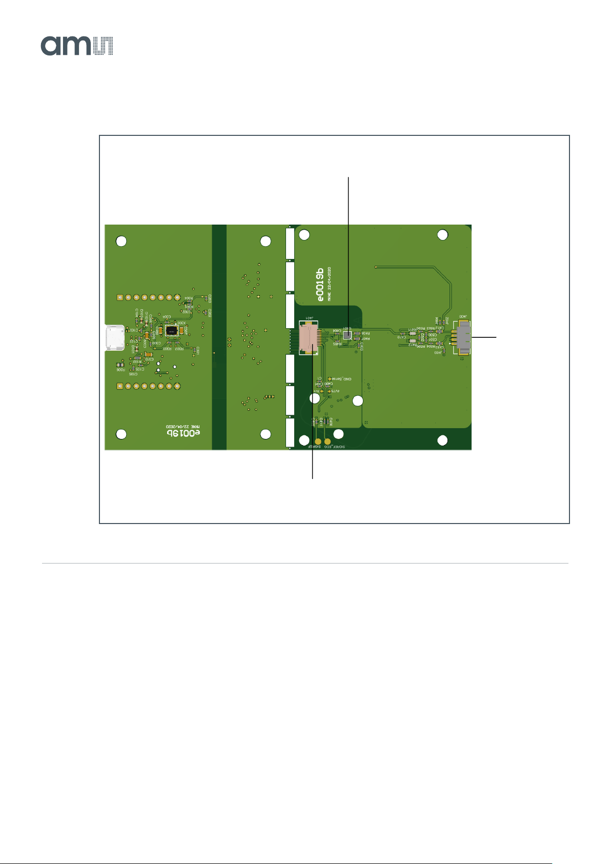
3.1 Hardware Architecture .................................7
3.2 Power Supply............................................... 8
4AS7030B Overview........................9
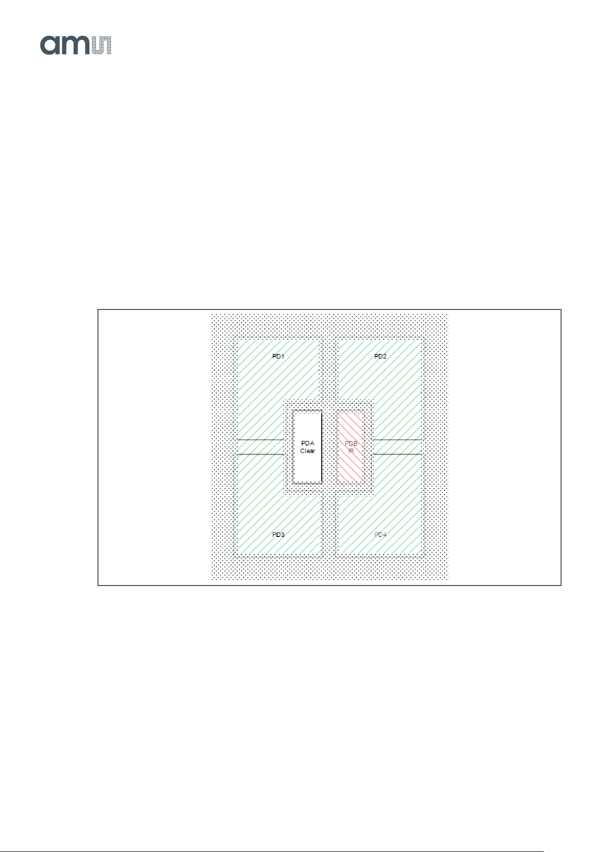
4.1 Optical Front End (OFE) .............................. 9
4.2 ECG Amplifier............................................. 12
4.3 Electrical Analog Front End (EAFE)........... 14
4.4 Light-to-Frequency Converter (LTF) .......... 15
4.5 ADC and FIFO ........................................... 15
4.6 Digital Interface.......................................... 17
4.7 Sampling Sequencer.................................. 17
5Software Description................... 23
5.1 Software Architecture................................. 23
5.2 Graphical User Interface............................ 27
5.3 FW, Driver, API.......................................... 55
6Revision Information................... 62
7Legal Information ........................ 63

Document Feedback
AS7030B
Introduction
Demo Kit Manual •PUBLIC
UG000493 •v1-00 • 2020-Jun-25
63 │3
1 Introduction
The AS7030B Evaluation Kit allows evaluation of all functions on the AS7030B Biosensor and test
them in various applications.
The initial Evaluation Kit works with USB connection to the PC and comes with a GUI, which enables
the user to change AS7030B register settings, see measurement results and many more.
The SDK (Software Development Kit) currently contains algorithms for HRM, HRV and BP and is
supplied with the Evaluation Kit. The compiled firmware can be flashed onto the STM32 ARM Cortex-
M4 low power MCU.
1.1 Kit Content
Figure 1:
Evaluation Hardware Board
For full flexibility, the vital signs sensor (AS7030B), an accelerometer (LIS2DH12) and three
electrodes are located on the break out board, which can be used in any application and re-connected
to the main board via FPC cable once broken off. There is also the option to attach external
electrodes. If you are using an optional Wristband evaluation kit, AS7038 wristband needs to be
connected to the Wristband PicoBlade connector K500 on Mainboard and sensor part of the kit need
to be separated from Mainboard.
Any signals important for development are accessible for probing at pin headers.

Document Feedback
AS7030B
Getting Started
Demo Kit Manual •PUBLIC
UG000493 •v1-00 • 2020-Jun-25
63 │5
2 Getting Started
The client software latest version is available for download at https://ams.com/as7030B#tab/tools or
the software is possible to find on the USB stick as a part of the evaluation kit. To install, start the
installer executable and follow the instructions as shown in Figure 2 (left to right top to bottom).
Figure 2:
AS7030B Vital Signs Sensor Installation

Document Feedback
AS7030B
Getting Started
Demo Kit Manual •PUBLIC
UG000493 •v1-00 • 2020-Jun-25
63 │6
For Windows OS versions prior to Windows®10, the STSW-STM32102 virtual COM port driver needs
to be installed as well. The driver can be found in the <drivers\STM32_vcp_driver> folder contained
within the client software installation path. To install it, go to your OS version directory (Win7 or Win8,
OS versions prior to Windows®7 are compatible with the Windows®7), then:
1. Double click on dpinst_x86.exe if you are running a 32-bits OS version
2. Double click on dpinst_amd64.exe if you are running a 64-bits OS version
3. Follow the instructions
For updating the FW on the evaluation board over USB, the DfuSe driver from STMicroelectronics has
to be installed. This is available in the <drivers\DFU> folder contained within the client software
installation path. To install it, go to your OS version directory (Win7, Win8 or Win8.1), then:
1. Go to [x86] directory or [x64] directory based on your OS version:
2. Double click on dpinst_x86.exe if you are running a 32-bits OS version
3. Double click on dpinst_amd64.exe if you are running a 64-bits OS version
4. Follow the instructions
Information
In some cases, it can be necessary that the driver needs to be installed even on a Windows 10
system. In this case chose the driver installer from the Win 8.1 folder and install.

Document Feedback
AS7030B
Hardware Description
Demo Kit Manual •PUBLIC
UG000493 •v1-00 • 2020-Jun-25
63 │7
3 Hardware Description
3.1 Hardware Architecture
Figure 3:
Evaluation Hardware Board –Top View
SWD
Interface IEC 60601
Compilant DC-DC
converter AS7030
ECG INN Electrode
ECG REF Electrode
ECG INP Electrode
Break Out Line
Test Point for External ECG REF Electrode
Test Point for External ECG INN Electrode
Test Point for External ECG INP Electrode
STM32L476RET6
MCU Isolators for all
Signals
Pin Header
DFU Button
Micro USB
Pin Header
Current
Consumption
ADC ADS114
Connector for
Sensor Board
Molex PN:
53261_1071, 10
Contacts

Document Feedback
AS7030B
Hardware Description
Demo Kit Manual •PUBLIC
UG000493 •v1-00 • 2020-Jun-25
63 │8
Figure 4:
Evaluation Hardware Board –Bottom View
3.2 Power Supply
The AS7030B Eval Kit is supplied by the USB connection. In order to avoid a direct connection from
the electrodes to the power grid, an IEC 60601-1 compliant RECOM DCDC converter (R0.25S-0505/H
or R0.25S-0505/HP) is assembled on the board as well as isolator ICs for all signals passing to the
sensor board. This means that there is no galvanic connection between the sensor board and the
power grid.
Accelerometer
LIS2DH12
Connector for
External
Electrodes
Connector for
Break out Board

Document Feedback
AS7030B
AS7030B Overview
Demo Kit Manual •PUBLIC
UG000493 •v1-00 • 2020-Jun-25
63 │9
4 AS7030B Overview
The AS7030B is a photocurrent and voltage sensor capable of taking PPG, ECG, proximity and skin
temperature/resistivity measurements. It integrates an optical front end, ECG amplifier, electrical
analog front end and light to frequency (LTF) converter. It features a built-in sampling sequencer, 128-
byte FIFO, a 14-bit SAR ADC, four GPIO pins and an I2C interface.
4.1 Optical Front End (OFE)
The figure below shows the block diagram of the optical front end.
Figure 5:
Optical Front End

Document Feedback
AS7030B
AS7030B Overview
Demo Kit Manual •PUBLIC
UG000493 •v1-00 • 2020-Jun-25
63 │10
The optical front end consists of:
●4 LED drivers, individually configurable, operated manually or controlled by the built-in sampling
sequencer
●2 built-in green LEDs (VD1 and VD2)
●1 built-in IR LED (VD4)
●1 free for connecting an external LED to VD3
●6 photodiodes
●4 with green filters (PD1, PD2, PD3 and PD4)
●1 with IR filter (B) (PD5)
●1 Clear (A) (PD6)
Figure 6:
Photodiode Arrangement

Document Feedback
AS7030B
AS7030B Overview
Demo Kit Manual •PUBLIC
UG000493 •v1-00 • 2020-Jun-25
63 │11
Trans-Impedance Amplifier (TIA)
●Configurable photodiode connection
●Photodiode input current offset compensation
●Configurable gain
●2 different modes of operation –photocurrent to voltage converter or photocurrent integrator
●Clip detection
Figure 7:
Trans-Impedance Amplifier
●TIA output filter (Prefilter, see Figure 8)
●Adjustable anti-aliasing low-pass filter
●Configurable high-pass filter to remove DC component
●Adjustable gain stage
●Clip detection
●2 identical signal conditioning blocks (OFE1 and OFE2, see Figure 8)
●Synchronous demodulator –Used to extract small optical signals in noisy environment
(ambient light)
●Adjustable synchronous demodulator output low pass filter
●Adjustable high pass filter for DC component removal
●50/60 Hz notch filter
●Adjustable output gain stage
●Adjustable low pass OFE1/2 output anti-aliasing filter (Figure 8)

Document Feedback
AS7030B
AS7030B Overview
Demo Kit Manual •PUBLIC
UG000493 •v1-00 • 2020-Jun-25
63 │12
Figure 8:
Optical Signal Conditioning
Each of the blocks depicted on Figure 8 can be individually enabled or disabled/bypassed.
4.2 ECG Amplifier
The ECG (electro cardiogram) amplifier is a high impedance, low noise instrumentation amplifier with
analog circuitry to band pass filter the signal. Gain is distributed between 3 gain stages. The gain in
the first stage determines the tradeoff between achievable noise level and achievable input offset
voltage. With the highest gain of 4 at the first gain stage (G1) about 400 mV of offset can be managed.
This value scales up to a max of 1.6 V of offset at gain 1. An optional 50/60 Hz notch filter can be
enabled to attenuate unwanted noise from mains coupling.
The recommended gain settings are 4-6-8 and 4-6-16

Document Feedback
AS7030B
AS7030B Overview
Demo Kit Manual •PUBLIC
UG000493 •v1-00 • 2020-Jun-25
63 │13
Figure 9:
ECG Amplifier Circuit
Figure 10:
Recommended ECG Frontend Filter
to electrical
frontend
Leads off
detect
ecg_ref_en
SIGREF
ecg_low_leakage_en for diode leakage
reduction on ECG_INP and ECG_INN
1G=1..128
SIGREF
ADC
800Hz
G_ina=18
(programmable 1 .. 48)
Ga i n Stage
Sta ge1 Di fferential
Ampl ifier
Sta ge2
Hi gh Pass Filter
Filter Gain
1 .. 41 .. 12
G2
G1
0.33Hz 50 Hz 40-200 Hz
Notch
Fi lter
Low Pa ss
Fi lter
Anti Aliasing
Fi lter
800 Hz
Instrumentational
Amplifier
AS7030_ECG_INP
AS7030_ECG_INN
AS7030_ECG_REF
ECG
Electrodes
ECG_INP
ECG_INN
ECG_REF

Document Feedback
AS7030B
AS7030B Overview
Demo Kit Manual •PUBLIC
UG000493 •v1-00 • 2020-Jun-25
63 │14
4.3 Electrical Analog Front End (EAFE)
The four general-purpose pins and ECG_REF can be used as analog input pins for the electrical
analog front end.
The analog inputs configuration sets up different non-inverting amplifier topologies:
●With offset and input voltage divider (temperature sensor)
●With current source and offset (temperature sensor)
●With current source and reference path (temperature sensor)
●With high impedance, GND referenced
●With DC-Blocking, referenced to V_ADCRef/2
●With DC-blocking and fast settling time, referenced to ADCRef /2
Figure 11:
Electrical Analog Front End

Document Feedback
AS7030B
AS7030B Overview
Demo Kit Manual •PUBLIC
UG000493 •v1-00 • 2020-Jun-25
63 │15
4.4 Light-to-Frequency Converter (LTF)
The LTF module can use any of the photodiodes. Photodiodes connected to the LTF cannot be used
at the same time with TIA. Integration time (itime) is configured in unit steps, one unit step is 3.702 ms.
The unit step can be reduced by 2, 4 or 8, this also reduces the resolution of the conversion. The LTF
modulator can be set to run continuously and write the result of each integration to the FIFO.
Figure 12:
Light-to-Frequency Converter
4.5 ADC and FIFO
4.5.1 ADC
The ADC is a 14-bit successive approximation register type with input clock of 1 MHz. A configurable
clock divider can reduce the input clock. One conversion takes 25 clock cycles plus configurable
number of ADC settling clock cycles (64 the default for ADC settling cycles).The ADC can be manually
triggered by register or automatically triggered by the built-in sampling sequencer. Two channel
selection registers ADC_CHANNEL_MASK_L and ADC_CHANNEL_MASK_H define the channels the
ADC will convert. The ADC will start with the channels in ADC_CHANNEL_MASK_L from the LS
asserted bit to the MS asserted bit, then continue with the channels in ADC_CHANNEL_MASK_H
register again from LS asserted bit to MS asserted bit. Then wraps back to the LS bit of
ADC_CHANNEL_MASK_L. Thus, the ADC will go through each channel in the order as shown in
Figure 13 with TIA being the first (smallest index), OFE1 second, SD1 third and so on to the GPIO2
being the last.

Document Feedback
AS7030B
AS7030B Overview
Demo Kit Manual •PUBLIC
UG000493 •v1-00 • 2020-Jun-25
63 │16
When triggered from the sequencer, the channel selection is always set to the smallest channel when
the sequencer starts for the first time. When sequencer starts, then stops and starts again, channel
selection will not reset, it will stay at the channel it was on when the sequencer stopped.
When triggered manually, the channel selection resets with every write to one of the channel selection
registers.
After each conversion, the sample goes to the FIFO and the channel selection automatically advances
to the next enabled channel. The current ADC output is also available in the ADC data register, but as
there is no latch mechanism, the data from this register can be inconsistent as the ADC might be
running at the time of ADC data register access.
ADC can trigger an interrupt after conversion has finished.
Figure 13:
ADC Channels
4.5.2 FIFO
The AS7030B FIFO is 256 bytes long. ADC samples are 2 bytes each, which means, FIFO can hold
up to 128 samples. There is a FIFO length register, which indicates how much samples are currently

Document Feedback
AS7030B
AS7030B Overview
Demo Kit Manual •PUBLIC
UG000493 •v1-00 • 2020-Jun-25
63 │17
available in the FIFO. The FIFO can send an interrupt when the number of available samples reaches
a certain configurable threshold.
4.6 Digital Interface
4.6.1 GPIO Pins
All four GPIO pins can be digitally controlled and can have pull up/down enabled. They can also be
used as analog input pins for the EAFE, GPIO2 and GPIO3 can additionally be used with the ADC.
4.6.2 Interrupts
An interrupt output pin INT is used to interrupt the host. Depending on the setting in register INTENAB
each of the interrupt source below can assert INT output pin (active low).
●irq_adc: End of ADC conversion
●irq_sequencer: End of sequencer sequence reached.
●irq_ltf: A light-to-frequency conversion is finished.
●irq_adc_threshold: ADC threshold triggered
●irq_fifothreshold: FIFO almost full (as defined in register fifo_threshold)
●irq_fifooverflow: FIFO overflow (error condition, data is lost)
●irq_clipdetect: TIA output and/or SD output exceeded threshold–see details in CLIPSTATUS
●irq_led_supply_low: LED supply low comparator triggered
4.7 Sampling Sequencer
The sampling sequencer synchronizes the LED pulsing, the synchronous demodulator, the ADC and
the integrator times. The sequencer configuration sets the LED on and off times, synchronous
demodulator positive and negative multiplication times, the ADC start time and the integrator start and
stop times. The sequencer generates the 8-bit timings based on the 1 μs input clock. The input clock
can be reduced with a configurable clock divider.
The sequencer executes measurement cycles with a period defined by Equation 1 where SEQ_PER
and SEQ_DIV are registers of AS7030B having values from 0 to 255 (see pages 50 and 51 in the
AS7030B datasheet):
Equation 1:
𝑆𝐸𝑄_𝑃𝐸𝑅 ∗ (𝑆𝐸𝑄_𝐷𝐼𝑉 + 1) ∗ 1𝜇𝑠
SEQ_DIV holds the value of the 1 µs input clock divider.

Document Feedback
AS7030B
AS7030B Overview
Demo Kit Manual •PUBLIC
UG000493 •v1-00 • 2020-Jun-25
63 │18
Within one sequencer cycle, the sequencer will:
●Switch on the LEDs at the specified LED start time and then switch them off at the LED stop
time.
●Start the positive and negative synchronous modulator multiplications at the specified start and
stop times for each operation
●Trigger a conversion of the currently selected ADC channel at the time specified by the ADC
start time. After the conversion has finished, ADC channel selection will advance the next
enabled ADC channel, which is measured during the next cycle that gives one ADC channel per
sequencer cycle. For the TIA channel, two additional ADC timings can be specified. That means
TIA can be measured up to 3 times within the same sequencer cycle:
●A 2nd measurement will be done, if the value for “2nd TIA” is specified (> 0) and is greater
than the one given in “1st” plus the time needed for the ADC to finish one conversion.
●A 3rd measurement will be done, if “3rd TIA” value is specified (> 0) and is greater than the
one given in “2nd TIA” plus the time needed for the ADC to finish one conversion.
●In the case of more than one TIA measurement within the same sequencer cycle, it is
important to make sure that the additional measurements can finish within the time of one
sequencer cycle.

Document Feedback
AS7030B
AS7030B Overview
Demo Kit Manual •PUBLIC
UG000493 •v1-00 • 2020-Jun-25
63 │19
Figure 14:
Sequencer Block Diagram
4.7.1 Sampling Rate and Subsampling
Throughout this document, sampling rate refers to the rate at which the sequencer produces samples
of the same ADC channel. This depends on the number of enabled ADC channels and on
configuration of the subsampling feature of the sequencer.
Subsampling is used when the application requires lower sample rates than what is possible with the
configured SEQ_PER and SEQ_DIV values, and with the number of enabled ADC channels. Lower
sample rate can also be achieved by setting SEQ_PER and SEQ_DIV to large enough values, but this
is not advisable as SEQ_DIV is multiplied to all the timings of the sequencer, thus the LED pulses will
become very long, which is probably not desired. SEQ_DIV should be kept relatively small for finer
resolution of the times.

Document Feedback
AS7030B
AS7030B Overview
Demo Kit Manual •PUBLIC
UG000493 •v1-00 • 2020-Jun-25
63 │20
The register SEQ_CFG and SD_SUBS configure how subsampling will be executed:
●sd_subs field in SD_SUBS register defines if subsampling is enabled; when it is 0, no
subsampling is done –every sequencer cycle triggers an ADC measurement (Figure 15);
setting to N>0, enables subsampling and then for N sequencer cycles the sequencer will not
trigger the ADC, followed by one cycle with ADC conversion.
●sd_subs_always bit in SEQ_CFG register defines if all enabled ADC channels are subject to
subsampling. Using this only makes sense for more than one enabled ADC channel.
●sd_subs_always = 1: subsampling of all enabled ADC channels (Figure 16)
●sd_subs_always = 0: subsampling of the first enabled ADC channel only (Figure 17)
The following three figures below show how subsampling is executed by the sequencer. In all of them
ADC cycle means one ADC iteration through all the enabled channels.
Attention
ADC cycle is not the same as sequencer cycle. ADC_SEL is the ADC channel selection;
ADC_ACCESS is an ADC conversion of the currently selected ADC channel; tADC is the configured
ADC start time in the sequencer configuration; tSUB is the sequencer period given by Equation 1.
In Figure 15 three ADC channels are enabled - 1 (OFE1), 6 (EAFE) and 11 (GPIO2). No subsampling
enabled (sd_subs=0).
In Figure 16 three ADC channels are enabled –0 (TIA), 4 (SD2) and 8 (ECGO). Subsampling is
enabled, every second sequencer cycle will trigger the ADC (sd_subs=2) and all enabled ADC
channels are subsampled.
In Figure 17 three ADC channels are enabled –0 (TIA), 4 (SD2) and 8 (ECG0). Subsampling is
enabled, every third sequencer cycle will trigger ADC (sd_subs=3) and only the first enabled ADC
channel is subsampled.
This manual suits for next models
1
Table of contents
Other AMS Motherboard manuals

AMS
AMS JetCis 130 User manual

AMS
AMS AS621 Series User manual

AMS
AMS USB I&P Box User manual

AMS
AMS AS703X_EVALKIT_BT User manual

AMS
AMS T 2672 Series User manual

AMS
AMS AS7058 User manual

AMS
AMS TSL2572 EVM User manual

AMS
AMS TCS3 7 Series User manual

AMS
AMS AS726x-iSPI User manual

AMS
AMS AS5-Series-47 User manual