AMS AS703X_EVALKIT_BT User manual

Document Feedback
AS7030B/AS7038GB/AS7038RB
Content Guide
Eval Kit Manual•PUBLIC
UG001014 •v1-00 • 2021-May-06
53 │2
Content Guide
1Introduction ................................... 3
1.1 Kit Content....................................................3
1.2 Ordering Information ....................................4
2Getting Started .............................. 5
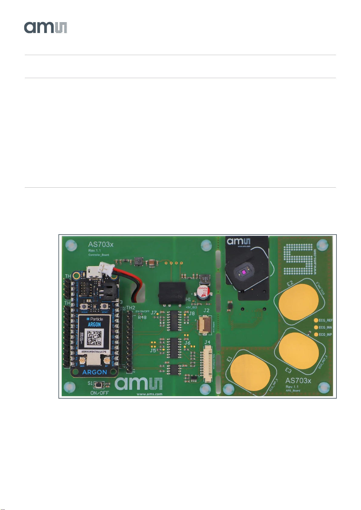
3Hardware Description ................... 6
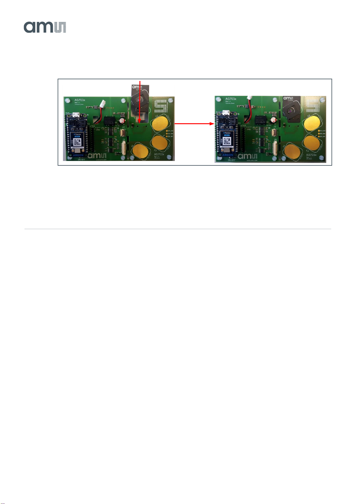
3.1 Hardware Architecture..................................6
3.2 Power Supply ...............................................8
4AS7030B/AS7038GB/AS7038RB
Overview ........................................ 9
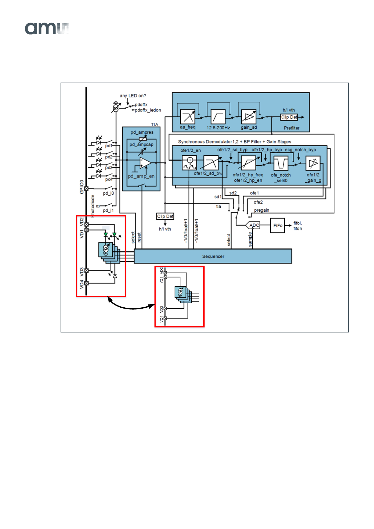
4.1 Optical Front End (OFE)...............................9
4.2 ECG Amplifier.............................................14
4.3 Electrical Analog Front End (EAFE)...........16
4.4 Light-to-Frequency Converter (LTF) ..........17
4.5 ADC and FIFO............................................17
4.6 Digital Interface...........................................19
4.7 Sampling Sequencer ..................................19
5Software Description...................25
5.1 Software Architecture .................................25
5.2 Graphical User Interface.............................26
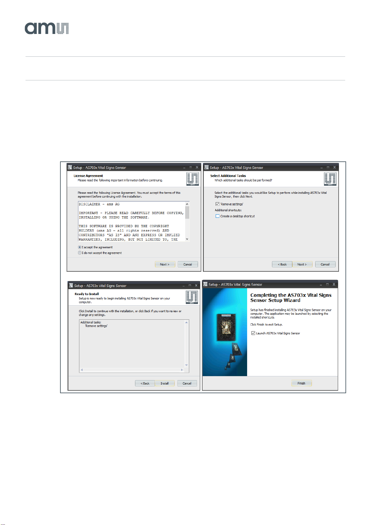
5.3 AS703x Firmware Upgrade........................48
6Revision Information...................52
7Legal Information.........................53

Document Feedback
AS7030B/AS7038GB/AS7038RB
Introduction
Eval Kit Manual •PUBLIC
UG001014 •v1-00 • 2021-May-06
53 │3
1 Introduction
The AS7030B/AS7038GB/AS7038RB Evaluation Kit allows evaluation of all functions on the
AS7030B/AS7038GB/AS7038RB Biosensor and test them in various applications.
The initial Evaluation Kit works with USB connection to the PC and comes with a GUI, which enables
the user to change AS7030B/AS7038GB/AS7038RB register settings, see measurement results and
many more.
The Windows GUI software is part of the kit and currently shows the raw data from FIFO with AGC
(Automatic Gain Control) features only. The Evaluation kit also contains firmware. New versions of the
firmware can be flashed onto the ARGON wireless module with an nRF52480 MCU.
1.1 Kit Content
Figure 1:
Evaluation Hardware Board
For full flexibility, the PCB of the evaluation kit has two parts: a controller boards and sensor board
(submodule or SMOD). The controller board has an accelerometer, three electrodes located and a
connector to interface with the submodule located on the breakout board. The break out part can be
re-connected to the Microcontroller part via an FPC cable if it is broken off.
AS7030B/AS7038GB/AS7038RB SMOD sensor board should be connected for the application

Document Feedback
AS7030B/AS7038GB/AS7038RB
Introduction
Eval Kit Manual •PUBLIC
UG001014 •v1-00 • 2021-May-06
53 │4
purposes. There is also an option to attach external electrodes. If an optional Wristband evaluation kit
is used, the AS7030B/AS7038GB/AS7038RB wristband needs to be connected to the Wristband Pico
Blade connector J502 on the Mainboard. As a result, the sensor part of the kit needs to be separated
from the Mainboard.
Any signals important for development are accessible for probing at pin headers.
1.2 Ordering Information
Ordering Code
Description
AS703X_EVALKIT_BT
Evaluation Kit for AS7030B/AS7038GB/AS7038RB
AS7030B_WRISTBAND
Wristband to connect to AS703x EvalKit
AS7038GB_WRISTBAND
Wristband to connect to AS703x EvalKit
AS7038RB_WRISTBAND
Wristband to connect to AS703x EvalKit

Document Feedback
AS7030B/AS7038GB/AS7038RB
Getting Started
Eval Kit Manual •PUBLIC
UG001014 •v1-00 • 2021-May-06
53 │5
2 Getting Started
The client software latest version is available for download at https://ams.com/as7030B#tab/tools or
https://ams.com/as7038GB#tab/tools or https://ams.com/as7038RB#tab/tools or the software is
possible to find on the USB stick as a part of the evaluation kit. To install, just double as shown in
Figure 2 (left to right, top to bottom)
Figure 2:
AS703x Software Installation
For updating the FW on the evaluation board over USB, please refer to chapter 5.3.1 for more details.

Document Feedback
AS7030B/AS7038GB/AS7038RB
Hardware Description
Eval Kit Manual •PUBLIC
UG001014 •v1-00 • 2021-May-06
53 │6
3 Hardware Description
3.1 Hardware Architecture
Figure 3:
AS703x Controller Board –Top View
Wireless Module IEC 60601
Compilant DC-DC
converter SMOD Interface
ECG INN Electrode
ECG REF Electrode
ECG INP Electrode
Break Out Line
Test Point for External ECG REF Electrode
Test Point for External ECG INN Electrode
Test Point for External ECG INP Electrode
Sensor on/off
Button
Isolators for all
Signals Connector for
Sensor Board

Document Feedback
AS7030B/AS7038GB/AS7038RB
Hardware Description
Eval Kit Manual •PUBLIC
UG001014 •v1-00 • 2021-May-06
53 │7
Figure 4:
AS703x Controller Board –Bottom View
Figure 5:
SMOD703xx –Top View
Current
Measurement
ADC ADS114
Connector for
External
Electrodes
Connector for
Break out Board SMOD module
Connector
External
IR LEDs
External
RED LEDs
External
GREEN LEDs
Internal
LEDs
Connector for AS703x
Controller Board
AS7030B
AS7038GB AS7038RB

Document Feedback
AS7030B/AS7038GB/AS7038RB
Hardware Description
Eval Kit Manual •PUBLIC
UG001014 •v1-00 • 2021-May-06
53 │8
Figure 6:
Fitting the SMOD703xx Sensor Board with the AS703x Controller Board
●The controller board supports AS7030B, AS7038GB & AS7038RB SMOD boards.
●The SMOD board should be mounted very carefully as shown in the Figure 6.
●During the mounting or changing of the SMOD board, the controller board should be turned off.
●Always mount the optical adapter on the top on the chip.
3.2 Power Supply
The AS7030B/AS7038GB/AS7038RB Eval Kit is supplied by the USB connector on the wireless
module. In order to avoid a direct connection from the electrodes to the power grid, an IEC 60601-1
compliant RECOM DCDC converter (R1SE - 3.305/H2) is assembled on the board as well as isolator
ICs for all signals passing to the sensor board. This means that there is no galvanic connection
between the sensor board and the power grid.
Board is Ready
Push

Document Feedback
AS7030B/AS7038GB/AS7038RB
AS7030B/AS7038GB/AS7038RB Overview
Eval Kit Manual •PUBLIC
UG001014 •v1-00 • 2021-May-06
53 │9
4 AS7030B/AS7038GB/AS7038RB Overview
Based on the optical filter and photodiode size, there are three types of AS703xxB sensors. AS7030B
& AS7038GB are most sensitive to green/IR light, and AS7038RB is most sensitive to red/IR light. On
the other hand, AS7030B has internal LEDs (two greens and one IR LED), but AS7038GB/RB
supports only external LEDs.
The operation of the AS7030B/AS7038GB/AS7038RB is based on photoplethysmography (PPG) and
electrocardiogram (ECG). PPG is the most used HRM method, which measures the pulse rate by
sampling light modulated by the blood vessels, which expand and contract as blood pulses through
them. ECG is the reference for any measurement of the biopotential generated by the heart.
Additionally, AS7038RB can measure blood oxygen saturation (SpO2).
In addition, the AS7030B/AS7038GB/AS7038RB devices also provide interfaces to external sensors.
These integrate an optical front end, ECG amplifier, electrical analog front end, and light to frequency
(LTF) converter. Features a built-in sampling sequencer, 128-byte FIFO, a 14-bit SAR ADC, four
GPIO pins, and an I²C interface.
Information
The main architecture of the AS703xxB sensor series is the same except a LED configurations,
●AS7030B has internal LEDs but AS7038GB/RB does not.
In this User Guide, the complete AS703xxB sensor series will be explained. Therefore, the chip
number will be emphasized if the dedicated part will come during the explanation. If there is no chip
number is mentioned in a chapter or portion of the chapter, that implies all the chips.
4.1 Optical Front End (OFE)
The Figure 7 below shows the block diagram of the optical front end.

Document Feedback
AS7030B/AS7038GB/AS7038RB
AS7030B/AS7038GB/AS7038RB Overview
Eval Kit Manual •PUBLIC
UG001014 •v1-00 • 2021-May-06
53 │10
Figure 7:
Optical Front End
For AS7030B
The optical front end consists of:
●4 LED drivers, individually configurable, operated manually or controlled by the built-in sampling
sequencer
●2 built-in green LEDs (VD1 and VD2)
●1 built-in IR LED (VD4)
●1 free for connecting an external LED to VD3
●6 photodiodes
●4 with green filters (PD1, PD2, PD3 and PD4)
●1 with IR filter (B) (PD5)
●1 Clear (A) (PD6)
AS7030B
AS7038GB/RB

Document Feedback
AS7030B/AS7038GB/AS7038RB
AS7030B/AS7038GB/AS7038RB Overview
Eval Kit Manual •PUBLIC
UG001014 •v1-00 • 2021-May-06
53 │11
Figure 8:
Photodiode Arrangement for AS7030B
For AS7038GB / AS7038RB
The optical front end consists of:
●4 LED drivers, individually configurable, operated manually or controlled by the built-in
sequencer
●6 photodiodes
●4 with green filters (PD1, PD2, PD3, and PD4) (If AS7038GB)
4 with RED/IR filters (PD1, PD2, PD3, and PD4) (If AS7038RB)
●1 with IR filter (B) (PD5)
●1 Clear (A) (PD6)

Document Feedback
AS7030B/AS7038GB/AS7038RB
AS7030B/AS7038GB/AS7038RB Overview
Eval Kit Manual •PUBLIC
UG001014 •v1-00 • 2021-May-06
53 │13
Trans-Impedance Amplifier (TIA)
●Configurable photodiode connection
●Photodiode input current offset compensation
●Configurable gain
●2 different modes of operation –photocurrent to voltage converter or photocurrent integrator
●Clip detection
Figure 10:
Trans-Impedance Amplifier
●TIA output filter (Prefilter, see Figure 11)
●Adjustable anti-aliasing low-pass filter
●Configurable high-pass filter to remove DC component
●Adjustable gain stage
●Clip detection
●2 identical signal conditioning blocks (OFE1 and OFE2, see Figure 11)
●Synchronous demodulator –Used to extract small optical signals in noisy environment
(ambient light)
●Adjustable synchronous demodulator output low pass filter
●Adjustable high pass filter for DC component removal
●50/60 Hz notch filter
●Adjustable output gain stage
●Adjustable low pass OFE1/2 output anti-aliasing filter (Figure 11)

Document Feedback
AS7030B/AS7038GB/AS7038RB
AS7030B/AS7038GB/AS7038RB Overview
Eval Kit Manual •PUBLIC
UG001014 •v1-00 • 2021-May-06
53 │14
Figure 11:
Optical Signal Conditioning
Each of the blocks depicted on Figure 11 can be individually enabled or disabled/bypassed.
4.2 ECG Amplifier
The ECG (electro cardiogram) amplifier is a high impedance, low noise instrumentation amplifier with
analog circuitry to band pass filter the signal. Gain is distributed between 3 gain stages. The gain in
the first stage determines the tradeoff between achievable noise level and achievable input offset
voltage. With the highest gain of 4 at the first gain stage (G1) about 400 mV of offset can be managed.
This value scales up to a max of 1.6 V of offset at gain 1. An optional 50/60 Hz notch filter can be
enabled to attenuate unwanted noise from mains coupling.
The recommended gain settings are 4-6-8 and 4-6-16

Document Feedback
AS7030B/AS7038GB/AS7038RB
AS7030B/AS7038GB/AS7038RB Overview
Eval Kit Manual •PUBLIC
UG001014 •v1-00 • 2021-May-06
53 │15
Figure 12:
ECG Amplifier Circuit
Figure 13:
Recommended ECG Frontend Filter
to electrical
frontend
Leads off
detect
ecg_ref_en
SIGREF
ecg_low_leakage_en for diode leakage
reduction on ECG_INP and ECG_INN
1G=1..128
SIGREF
ADC
800Hz
G_ina=18
(programmable 1 .. 48)
Gain Stage
Stage1 Differential
Amplifier
Stage2
Hi gh Pass Filter
Filter Gain
1 .. 41 .. 12
G2
G1
0.33Hz 50 Hz 40-200 Hz
Notch
Filter Low Pass
Filter Anti Aliasing
Filter
800 Hz
Instrumentational
Amplifier
AS7030_ECG_INP
AS7030_ECG_INN
AS7030_ECG_REF
ECG
Electrodes
ECG_INP
ECG_INN
ECG_REF

Document Feedback
AS7030B/AS7038GB/AS7038RB
AS7030B/AS7038GB/AS7038RB Overview
Eval Kit Manual •PUBLIC
UG001014 •v1-00 • 2021-May-06
53 │16
4.3 Electrical Analog Front End (EAFE)
The four general-purpose pins and ECG_REF can be used as analog input pins for the electrical
analog front end.
The analog inputs configuration sets up different non-inverting amplifier topologies:
●With offset and input voltage divider
●With current source and offset
●With current source and reference path
●With high impedance, GND referenced
●With DC-Blocking, referenced to V_ADCRef/2
●With DC-blocking and fast settling time, referenced to ADCRef /2
Figure 14:
Electrical Analog Front End

Document Feedback
AS7030B/AS7038GB/AS7038RB
AS7030B/AS7038GB/AS7038RB Overview
Eval Kit Manual •PUBLIC
UG001014 •v1-00 • 2021-May-06
53 │17
4.4 Light-to-Frequency Converter (LTF)
The LTF module can use any of the photodiodes. Photodiodes connected to the LTF cannot be used
at the same time with TIA. Integration time (itime) is configured in unit steps, one unit step is 3.702 ms.
The unit step can be reduced by 2, 4 or 8, this also reduces the resolution of the conversion. The LTF
modulator can be set to run continuously and write the result of each integration to the FIFO.
Figure 15:
Light-to-Frequency Converter
4.5 ADC and FIFO
4.5.1 ADC
The ADC is a 14-bit successive approximation register type with input clock of 1 MHz. A configurable
clock divider can reduce the input clock. One conversion takes 25 clock cycles plus configurable
number of ADC settling clock cycles (64 the default for ADC settling cycles).The ADC can be manually
triggered by register or automatically triggered by the built-in sampling sequencer. Two channel
selection registers ADC_CHANNEL_MASK_L and ADC_CHANNEL_MASK_H define the channels the
ADC will convert. The ADC will start with the channels in ADC_CHANNEL_MASK_L from the LS
asserted bit to the MS asserted bit, then continue with the channels in ADC_CHANNEL_MASK_H
register again from LS asserted bit to MS asserted bit. Then wraps back to the LS bit of
ADC_CHANNEL_MASK_L. Thus, the ADC will go through each channel in the order as shown in
Figure 16 with TIA being the first (smallest index), OFE1 second, SD1 third and so on to the GPIO2
being the last.

Document Feedback
AS7030B/AS7038GB/AS7038RB
AS7030B/AS7038GB/AS7038RB Overview
Eval Kit Manual •PUBLIC
UG001014 •v1-00 • 2021-May-06
53 │18
When triggered from the sequencer, the channel selection is always set to the smallest channel when
the sequencer starts for the first time. When sequencer starts, then stops and starts again, channel
selection will not reset, it will stay at the channel it was on when the sequencer stopped.
When triggered manually, the channel selection resets with every write to one of the channel selection
registers.
After each conversion, the sample goes to the FIFO and the channel selection automatically advances
to the next enabled channel. The current ADC output is also available in the ADC data register, but as
there is no latch mechanism, the data from this register can be inconsistent as the ADC might be
running at the time of ADC data register access.
ADC can trigger an interrupt after conversion has finished.
Figure 16:
ADC Channels

Document Feedback
AS7030B/AS7038GB/AS7038RB
AS7030B/AS7038GB/AS7038RB Overview
Eval Kit Manual •PUBLIC
UG001014 •v1-00 • 2021-May-06
53 │19
4.5.2 FIFO
The AS7030B/AS7038GB/AS7038RB FIFO is 256 bytes long. ADC samples are 2 bytes each, which
means, FIFO can hold up to 128 samples. There is a FIFO length register, which indicates how much
samples are currently available in the FIFO. The FIFO can send an interrupt when the number of
available samples reaches a certain configurable threshold.
4.6 Digital Interface
4.6.1 GPIO Pins
All four GPIO pins can be digitally controlled and can have pull up/down enabled. They can also be
used as analog input pins for the EAFE, GPIO2 and GPIO3 can additionally be used with the ADC.
4.6.2 Interrupts
An interrupt output pin INT is used to interrupt the host. Depending on the setting in register INTENAB
each of the interrupt source below can assert INT output pin (active low).
●irq_adc: End of ADC conversion
●irq_sequencer: End of sequencer sequence reached.
●irq_ltf: A light-to-frequency conversion is finished.
●irq_adc_threshold: ADC threshold triggered
●irq_fifothreshold: FIFO almost full (as defined in register fifo_threshold)
●irq_fifooverflow: FIFO overflow (error condition, data is lost)
●irq_clipdetect: TIA output and/or SD output exceeded threshold–see details in CLIPSTATUS
●irq_led_supply_low: LED supply low comparator triggered
4.7 Sampling Sequencer
The sampling sequencer synchronizes the LED pulsing, the synchronous demodulator, the ADC and
the integrator times. The sequencer configuration sets the LED on and off times, synchronous
demodulator positive and negative multiplication times, the ADC start time and the integrator start and
stop times. The sequencer generates the 8-bit timings based on the 1 μs input clock. The input clock
can be reduced with a configurable clock divider.
The sequencer executes measurement cycles with a period defined by Equation 1 where SEQ_PER
and SEQ_DIV are registers of AS7030B/AS7038GB/AS7038RB having values from 0 to 255 (see in
the AS7030B/AS7038GB/AS7038RB datasheet):

Document Feedback
AS7030B/AS7038GB/AS7038RB
AS7030B/AS7038GB/AS7038RB Overview
Eval Kit Manual •PUBLIC
UG001014 •v1-00 • 2021-May-06
53 │20
Equation 1:
𝑆𝐸𝑄_𝑃𝐸𝑅 ∗ (𝑆𝐸𝑄_𝐷𝐼𝑉 + 1) ∗ 1𝜇𝑠
SEQ_DIV holds the value of the 1 µs input clock divider.
Within one sequencer cycle, the sequencer will:
●Switch on the LEDs at the specified LED start time and then switch them off at the LED stop
time.
●Start the positive and negative synchronous modulator multiplications at the specified start and
stop times for each operation
●Trigger a conversion of the currently selected ADC channel at the time specified by the ADC
start time. After the conversion has finished, ADC channel selection will advance the next
enabled ADC channel, which is measured during the next cycle that gives one ADC channel per
sequencer cycle. For the TIA channel, two additional ADC timings can be specified. That means
TIA can be measured up to 3 times within the same sequencer cycle:
●A 2nd measurement will be done, if the value for “2nd TIA” is specified (> 0) and is greater
than the one given in “1st” plus the time needed for the ADC to finish one conversion.
●A 3rd measurement will be done, if “3rd TIA” value is specified (> 0) and is greater than the
one given in “2nd TIA” plus the time needed for the ADC to finish one conversion.
●In the case of more than one TIA measurement within the same sequencer cycle, it is
important to make sure that the additional measurements can finish within the time of one
sequencer cycle.
Table of contents
Other AMS Motherboard manuals

AMS
AMS TSL2584TSV User manual

AMS
AMS CCS811 User manual

AMS
AMS AS3933 Operating and installation instructions

AMS
AMS AS5 47 Series User manual

AMS
AMS AS5048 Eval-Kit Manual

AMS
AMS TMD2620 User manual

AMS
AMS AS5270-MF_EK_SB User manual

AMS
AMS TSL2541 User manual

AMS
AMS AN5000 Series Installation and operating instructions

AMS
AMS AS621 Series User manual