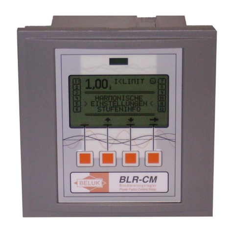
Beluk BLR-CM Modbus Guide

Technical Documentation
BLR-CM Modbus
Rev. 05
2018-09
Beluk GmbH
Taubenstrasse 1
86956 Schongau
Germany
Tel.: +49/(0)8861/2332-0
Fax: +49/(0)8861/2332-22
E-Mail: [email protected]
Web: http://www.beluk.de
Technical Documentation
BLR-CM Modbus

Technical Documentation
BLR-CM Modbus
Rev. 05
2018-09
2
Document history
Date
Name
Revision
Comment
08.11.06
ATh
01
initial document release
20.03.07
ATh
02
features of new software (V2.1.x)
21.09.07
Le
03
New connector on Modbus hardware
valid from firmware V 2.2.x
18.11.08
Le
04
Inserting additional bus address
24.09.18
SMi
05
Adaption to firmware V 2. 7.x
Layout changes

Technical Documentation
BLR-CM Modbus
Rev. 05
2018-09
3
Content
1OVERVIEW .......................................................................................................................................................... 4
2MODBUS/ RS485................................................................................................................................................. 5
2.1 RS485 (defined in EIA485/ISO8482)................................................................................................................. 5
2.1.1 Connection...................................................................................................................................................... 6
2.1.2 Line termination ............................................................................................................................................. 7
2.1.3 Line biasing ..................................................................................................................................................... 7
2.1.4 Communication indicator ............................................................................................................................... 7
2.2 The Modbus protocol ...................................................................................................................................... 8
2.2.1 Modbus - description...................................................................................................................................... 8
2.2.2 Serial data format ........................................................................................................................................... 8
2.2.3 Serial transmission modes .............................................................................................................................. 9
2.2.4 Function codes................................................................................................................................................ 9
2.2.5 Exception codes ............................................................................................................................................ 10
2.2.6 Master-Slave protocol .................................................................................................................................. 10
3BLR-CM MODBUS...............................................................................................................................................10
3.1 Setup..............................................................................................................................................................10
3.2 Address space ................................................................................................................................................10
3.3 Measurement values......................................................................................................................................11
3.4 Work counters ...............................................................................................................................................12
3.5 Parameter settings .........................................................................................................................................13
3.6 Stage status....................................................................................................................................................17
3.7 Device status..................................................................................................................................................18
3.8 Storage settings .............................................................................................................................................20
4TROUBLE SHOOTING ..........................................................................................................................................21

Technical Documentation
BLR-CM Modbus
Rev. 05
2018-09
4
Important information!
If this sign appears besides a text passage, the reader is strongly advised to read the corresponding information. It
may provide important information about the usage of the device, safety advices or information about the correct
handling of the device. If the information is disregarded, the device may be inoperable or even damaged!
Additional Modbus protocol can be found at www.modbus.org.
The Modbus standards are also available from there.
1Overview
The Modbus communication interface of the reactive power controller CM offers the possibility to read out
measurement values or adjusting settings. This can be done by remote computer systems.
Attention: The BLR-CM can send max. 30 Values per request
The present manual describes the data transmission using the Modbus protocol, which defines methods of data
transport and addressing, but does not generally determined a specific transmission medium (physical transmission
level).
The reactive power controller CM uses the industrial standard RS485 for data transmission. This bus system offers the
possibility to operate several devices at the same bus cable.
A multitude of commercial devices and programmable logic controllers (PLC) are compatible with the Modbus protocol,
which is why a bus system can be set up with little effort.
!

Technical Documentation
BLR-CM Modbus
Rev. 05
2018-09
5
2Modbus/ RS485
The communication protocol Modbus RTU basically includes two levels:
The RS485 industrial standard defines the data transmission medium. Here, the physical data byte transmission
between the bus participants is controlled. This part of the protocol is embedded in higher Modbus levels.
The Modbus application protocol uses the underlying RS485 protocol for data transmission. It defines
commands (“Function Codes”, FC), addresses and data structures.
2.1 RS485 (defined in EIA485/ISO8482)
The communication standard RS485 uses two wires for data transport D(+) and D(-). Signals are transmitted with a
differential voltage level of at least ± 200 mV. Thus, the two logical levels “low” and “high” are possible. Due to its
differential transmission technology, the standard RS485 is particularly resistant to electromagnetic interferences and
wire lengths of more than 1000 meters may be reached.
The reactive power controller CM is compatible with the following transmission rates: 1200; 2400; 4800; 19200; 38400;
57600 and 115200 baud. All parity variations (even, odd and none) are supported.
In the RS485 standard, two transmission variations are defined:
2-wire RS485: This type uses two wires for the communication, which is why the same wire pair is used for
both data directions. Therefore, it is necessary to switch between sending and receiving at each device (half-
duplex mode).
4-wire RS485: In this case, a single wire pair is used for each data direction. However, due to the Modbus
protocol, it is also only possible to use the half-duplex mode again. For this reason, it is not possible to increase
the transmission capacity.
The power factor controller CM supports 2-wire RS485 only!
Next to the data lines, a common ground (GND) line must be interconnect all bus participants. It is not allowed to use
the cable shield for this purpose. The shield must be connected to GND, in order to reduce electromagnetic influences.
According to the RS485 standard, up to 32 devices can be connected to a single bus segment. This is done by connecting
all devices in parallel. This concerns the data lines D(+) and D(-) as well as the GND line.
In order to connect more than 32 devices to a bus, a “Repeater” must be used to between the bus-segments.
Technical Documentation
BLR-CM Modbus
Rev. 05
2018-09
6
2.1.1 Connection
There are two Modbus interfaces:
a) 9-pin D-SUB
PIN1 +5V (For data line bias only. It is not allowed to supply external circuits by this pin!)
PIN2 Common ground (GND) for all bus participants.
PIN5 D (B) - Data signal B
PIN9 D (A) - Data signal A
b) 3-pin Connector
The power factor controller CM uses a 3-pin connector, which is
shown on the right side.
In order to establish a Modbus connection, the data lines + and - and
the common ground (middle pin) must be connected.
Attention: Various vendors uses the assignment A and B. Equating this designation (A = +) and (B = -) does not always
apply. This must be checked for each device.
5
4
3
2
1
9
8
7
6

Technical Documentation
BLR-CM Modbus
Rev. 05
2018-09
7
2.1.2 Line termination
The termination of the bus wire is strictly necessary, in order to prevent interferences and set up a stable connection.
For this reason, both wire ends of the bus must be terminated with a resistor. The value of the resistor must fit to the
cable impedance and is generally selected as 120 Ω. A resistor must be connected at each end of the bus-segment.
Some devices, particularly bus converters, include a termination resistor by default. Therefore, it is necessary to check
the user manuals of all implemented bus devices. If devices, with integrated termination resistor, are connected within
the bus segment, their termination resistors must be switched off. In case it is not possible to switch it off, the respective
devices must be placed at the ends of the bus! Consequently, it is only possible to use two devices with fix termination
resistors!
2.1.3 Line biasing
Without a bias voltage, the logic level in the data wires would be undefined while no data is transmitted. Additionally,
external influences may lead to interferences of the signal level. For this reason, line biasing is required.
This is done by two resistors, which must be in the range of 450 Ω…650 Ω. The first resistor is used as pull-up resistor
and is connected between the data wire + resp. D(+) and +5 V. The second resistor is used as pull-down resistor and is
connected between the data wire –resp. D(-) and 0 V. These resistors are required once per bus segment and their
position within the bus segments is freely selectable. However, it is recommend to select a position in the middle of the
bus wire. Before installing these resistors, it must be checked if the implemented devices already include integrated
bias resistors.
Attention: In case of the BLR-CM, a line bias voltage must be provided externally.
2.1.4 Communication indicator
The yellow LED on the backside of the device indicates an active transmission.
It only flashes, when the device is actually communicating with the bus
master.
The communication indicator LED is available for both connector variants.

Technical Documentation
BLR-CM Modbus
Rev. 05
2018-09
8
2.2 The Modbus protocol
2.2.1 Modbus - description
The Modbus protocol uses the RS485 as an underlying physical layer and implements the data transmission control
mechanisms. Therefore, it is located on layer 2 ("link layer") of the OSI layer model for data exchange systems.
2.2.2 Serial data format
The data is transmitted in fixed frames. The frames are separated by the bus being inactive for at least 3,5 characters.
All data is organized in "protocol data units" (PDUs), which are transmitted over the serial bus system by the underlying
physical protocol layer.
PDU
FC
data
1 byte
n bytes
Illustration 1 : "Protocol Data Unit" - PDU
The PDU consists of two parts:
The "function code" (FC) is a command, which defines how the slave has to respond.
The data block contains information, which correspond to the FC. Its usage depends on the FC, it can either
contain data or register addresses for slave data access.
The PDU defines a single data unit, which has to reach a certain bus device in order to perform an action. The type of
the transfer differs dependent on the physical layer.
To be able to control the transmission, the PDU is extended by two additional blocks. In RS485, the frame is now called
"application data unit" (ADU).
ADU
slave #
FC
data
CRC
1 byte
1 byte
n bytes
2 bytes
Illustration 2 : "Application Data Unit" - ADU

Technical Documentation
BLR-CM Modbus
Rev. 05
2018-09
9
The application data unit, contains two additional blocks of data:
The first field specifies the "slave number", which contains the slave address.
In order to secure the transmission, the las block includes a cyclic redundancy check (CRC) value.
2.2.3 Serial transmission modes
The protocol defines two different encodings for the frames' data contents. The RTU- and ASCII-coding.
Attention: The BLR-CM supports the RTU-mode only!
"Remote Terminal Unit" (RTU)
At this transmission mode, every 8-bit data word contains two 4-bit hexadecimal numbers. They are transmitted as
complete byte to reach a maximum transmission density. With every data word, the following information is
transmitted:
1 Start bit
8 Data bits, "least significant bit" first
1 Parity bit (if set)
1 Stop bit for parity even or odd / 2 if parity is none to compensate missing parity bit
2.2.4 Function codes
As it was mentioned before, the data packet contains "function codes", which specify a command from the bus master
to the bus slave. The slave executes the command (if possible) and answers with the same function code to acknowledge
the command. The valid function code range is specified from 1 to 127, but only a part of it is actually used. Please refer
to the Modbus specifications for detailed Information.
If it is impossible for a slave to execute a command, it replies with an error code (exception code). The function code of
an exception package is the function code itself and the most significant bit is set by the slave to signal the error
condition to the master. Moreover, the content of the data block specify the error in more detail.
The BLR-CM supports the function codes 03hex (read holding register), 04 hex (read input register) and 06hex (write single
register).

Technical Documentation
BLR-CM Modbus
Rev. 05
2018-09
10
2.2.5 Exception codes
If a slave is not able to execute a command, it answers with exception codes. A full list of codes can be found in the
Modbus specification. The corresponding list is not provided at this point, because the master software handles the
most exceptions automatically.
2.2.6 Master-Slave protocol
Since the master-slave protocol is used, only the bus master can initialize a transfer. The "master" starts an exchange
by sending data and the corresponding function code (=command) to the slave. Afterwards the slave executes the
command.
Usually, the unicast-mode is used to communicate within a Modbus system. Here, data packages are send to a
single slave, including its address. The valid address range is between 1 and 247. The slave executes the
command and answers by sending a acknowledge data package back to the master.
In multicast-mode all slaves on the bus are addressed in parallel. They all receive and execute the same
command, but none of them respond. The master initiates a multicast command by using "0" as slave number.
3BLR-CM Modbus
3.1 Setup
If the device supports Modbus, an additional entry is available in the “setup” - menu of the device. In this menu the
following settings can be done:
ADDRESS: This is the device’s slave address (slave ID). The valid range is 1-247.
BAUD RATE: Here, the baud rate can be selected. The valid range is 1200 - 115200 baud.
PARITY: The parity can be selected to be none, even or odd.
While baud rate and parity must be the same for all bus devices, the address must be unique for each device.
3.2 Address space
The data in the BLR-CM is organized and accessed by addresses. Each address accesses one data word. The size of a
data word is always 16 bit.
The BLR-CM does not differ between the addresses and the function codes. There is one big address space available
and in order to access each address’s data, any valid function code can be used. Nevertheless, the data will only make
sense when interpreted the correct way!

Technical Documentation
BLR-CM Modbus
Rev. 05
2018-09
11
The data can be of the following types:
FLOAT: 32 bit floating-point number, as it is defined in IEEE-754.
UINT16: Unsigned 16 bit integer value.
UINT32, SINT32: Unsigned/signed 32 bit integer value.
Since the data is organized in 16 bit wide words, a set of sequential addresses has to be read in order to get longer data
items. In this case, only the base address is given in the tables. For example, to read a FLOAT value with base address
12, two 16 bit words must be read (addresses 12 and 13). These two values need to be concatenated to form the desired
result of 32 bits. Most SCADA software packages or PLCs can do this automatically.
There exist different types of addresses:
The Modbus address always starts with 0 and can go up to 65535. It can be used with any
function code.
Certain PLCs cannot handle the address 0 and therefore add 1 to the address. So their
addresses system (Modbus address +1) always start with 1.
Some SCADA tools add an offset to determine the function code, which is used to access the
device at the given address. Sometimes, they also add 1 to the Modbus address.
As an example, the address 40001 would be “read Modbus address 0 with function code
03hex”, 30012 would be “read Modbus address 11 with function code 04hex”.
Please refer to the corresponding software’s manual to find the correct addresses.
Attention: The following tables always give the Modbus addresses mentioned first in above list.
3.3 Measurement values
The measured values are available in an interval of 2 data words, starting at address 0. All values can be accessed with
function codes 03hex and 04 hex..
If the current or voltage is too small to calculate valid harmonics, the value at the base address (= the fundamental) is
0.0%. This also indicates, that the higher harmonic current or voltage values are also invalid!
Attention: The values Apparent power sum, Active power sum, Reactive power sum, Lacking reactive power ΔQ and
Power factor (P/S) refere to a symmetrical power system.
!

Technical Documentation
BLR-CM Modbus
Rev. 05
2018-09
12
Address
Value
Words
Type
Unit
0
Frequency
2
FLOAT
Hz
2
Voltage phase –phase
2
FLOAT
V
4
Voltage phase - neutral
2
FLOAT
V
6
Current I1
2
FLOAT
A
18
Apparent power S-sum
2
FLOAT
VA
26
Active power P-sum
2
FLOAT
W
34
Reactive power Q-sum
2
FLOAT
var
42
Lacking reactive power ΔQ
2
FLOAT
var
50
Power factor (P/S)
2
FLOAT
-
58
Total harmonic distortion THD U
2
FLOAT
%
60
Harmonics U 1. order = fundamental wave
2
FLOAT
%
62
Harmonics U 2. order
2
FLOAT
%
64
Harmonics U 3. order
2
FLOAT
%
…
…
…
…
…
122
Harmonics U 32. order
2
FLOAT
%
124
Total harmonic distortion THD I
2
FLOAT
%
130
Harmonics I 1. order = fundamental wave
2
FLOAT
%
132
Harmonics I 2. order
2
FLOAT
%
134
Harmonics I 3. order
2
FLOAT
%
…
…
…
…
…
192
Harmonics I 32. order
2
FLOAT
%
322
Ambient temperature
2
FLOAT
°C
3.4 Work counters
In order to reach an accurate value, work counters/accumulators are arranged in a special way. Each counter consists
of two parts:
1. A FLOAT-type base counter which simply accumulates/integrates the power. If this counter reaches 1000000.0,
the extended counter is increased by one and 1000000.0 is subtracted from the base counter.
2. A LONG-type extended counter, which is used to count portions of MW / Mvar up to (232-1)106.
To get the real work value, the extended counter must be multiplied with 1000000 and afterwards the base counter
value must be added. This keeps the precision of the FLOAT-type base counter in acceptable range, because huge values
can be handled as well.

Technical Documentation
BLR-CM Modbus
Rev. 05
2018-09
13
All values can be accessed with function codes 03hex and 04 hex.
Address
Value
Words
Type
Unit
1792
WQ inductive –extended counter
2
UINT32
MVarh
1794
WQ inductive –base counter
2
FLOAT
Varh
1796
WQ capacitive –extended counter
2
UINT32
MVarh
1798
WQ capacitive –base counter
2
FLOAT
Varh
1800
WP import –extended counter
2
UINT32
MWh
1802
WP import –base counter
2
FLOAT
Wh
1804
WP export –extended counter
2
UINT32
MWh
1806
WP export –base counter
2
FLOAT
Wh
It is possible to read the work counters already summarized since firmware version 2.7.0. These values can be
accessed with function codes 03hex and 04 hex.
Address
Value
Words
Type
Unit
2048
WQ inductive
2
REAL
kVarh
2050
WQ capacitive
2
REAL
kVarh
2052
WP import
2
REAL
kWh
2054
WP export
2
REAL
kWh
3.5 Parameter settings
Parameters, which are set by the user, are stored in various data types. The base addresses and the data type can be
found in the table below.
All values can be accessed with function codes 03hex,04 hex and 06hex.
Address
Value
Words
Type
Unit
512
PT ratio x 10
1
UINT16
-
513
CT ratio x 10
1
UINT16
-
514
User parameters 1
1
UINT16
-
515
Phase correction
1
UINT16
°
517
Nominal voltage L - L
2
UINT32
V
519
Limit max. voltage
1
UINT16
%
520
Limit min. voltage
1
UINT16
%
522
Switching time delay x 10
1
UINT16
s
523
Target cos φ 1 (0..100..200 = i0.00..1.00..c0.00)
1
UINT16
-

Technical Documentation
BLR-CM Modbus
Rev. 05
2018-09
14
524
Target cos φ 2 (0...100…200 = i0.00...1.00…c0.00)
1
UINT16
-
525
control sensitivity
1
UINT16
%
526
Tolerance switch cycles balancing
1
UINT16
%
527
Alarm Enable Output Mask 1 (OM1)
1
UINT16
-
528
Alarm action: „Switch Alarm Relay (M)“ (OM1)
1
UINT16
-
529
Alarm action: „Switch DO-Relay (DO)“ (OM1)
1
UINT16
-
530
Alarm action: „Show Display Message (D)“ (OM1)
1
UINT16
-
531
Alarm action: „Target COS-PHI 2 (CP)“ (OM1)
1
UINT16
-
532
Alarm action: „Switch Controll off (O)“ (OM1)
1
UINT16
-
533
Alarm action: „Freeze Control (F)” (OM1)
1
UINT16
-
533
Limit alarm temperature 1 x 10
1
UINT16
°C
534
Limit alarm temperature 2 x 10
1
UINT16
°C
535
Hysteresis temperature x 10
1
UINT16
°C
536
Limit alarm THD U x 10
1
UINT16
%
537
Limit alarm THD I x 10
1
UINT16
%
539
Limit warning step size
1
UINT16
%
540
Limit warning switch cycles
2
UINT32
-
542
Limit alarm active power P
2
UINT32
W
544
Limit alarm reactive power Q
2
UINT32
var
546
pf alarm min (0...100...200 = i0.00...1.00...c0.00)
1
UINT16
-
547
pf alarm max (0...100...200 = i0.00...1.00...c0.00)
1
UINT16
-
548
pf alarm delay time
1
UINT16
s
555
Switching time delay Step exchange x 10
1
UINT16
s
556
Delay time fast control
1
UIN16
per
557
Max. step size (fast control)
1
UINT16
var
559
Mean Q. (fast control)
1
UINT16
Var
560
Datalogger storage interval (0…720)
(Only available with option –DM)
1
UINT16
Min
561
Fast Control Output Mask 1 (OM1)
(Only available with option 1PH: -06T, -12T, -12RT)
Note: Just the THD-U Bit is allowed
1
UINT16
-
562
Alarm frequency: lower limit
(450…(MaxValue-10) = 45,0Hz…(MaxValue-0,1Hz))
1
UINT16
Hz
563
Alarm frequency: upper limit
((MinValue+10)…650 = (MinValue+0,1Hz)...65,0Hz)
1
UINT16
Hz
564
Alarm Enable Output Mask 2 (OM2)
1
UINT16
-
565
Alarm action: „Switch Alarm Relay (M)“ (OM2)
1
UINT16
-
566
Alarm action: „Switch DO-Relay (DO)“ (OM2)
1
UINT16
-

Technical Documentation
BLR-CM Modbus
Rev. 05
2018-09
15
567
Alarm action: „Show Display Message (D)“ (OM2)
1
UINT16
-
568
Alarm action: „Target COS-PHI 2 (CP)“ (OM2)
1
UINT16
-
569
Alarm action: „Switch Controll off (O)“ (OM2)
1
UINT16
-
570
Alarm action: „Freeze Control (F)” (OM2)
1
UINT16
-
571
Language Setting
SW 02.07.xx:
Bit 0 =English, Bit 1 = German, Bit 2 = French
SW 02.08.xx:
Bit 0 =English, Bit 1 = Spanish, Bit 2 = Portuguese
1
UINT16
-
572
Asymmetry factor
1
SINT16
-
573
User parameters 2
1
UINT16
-
574
Q-Offset (-32000…32000 = -3200,0kvar…3200,0kvar)
1
SINT16
kvar
575
Temperature Offset (-100…100 = -10°C…10°C)
1
SINT16
°C
The addresses 514 (User parameters 1), 527 –533 (Alarm Output Mask 1), 561 (Alarm Output Mask 1), 564 –470 (Alarm
Output Mask 2) und 573 (User parameters 2) are coded binary. The assignment of the single bits is depicted in the
following tables.
User parameters 1
Bit 15
Bit 0
Bit 0
Synchronization Frequency
00 = Automatic
01 = Fix 50 Hz
10 = Fix 60 Hz
Bit 1
Synchronization Frequency
Bit 2
Measurement connection
1 = LL
0 = LN
Bit 3
Stage recognition
1 = Off
0 = On
Bit 4
Switch cycle distribution
1 = Yes
0 = No
Bit 5
Start AI count down (90 s after each restart)
1 = Yes
0 = No
Bit 6
1
1 = Yes
0 = No
Bit 7
Stage exchange
1 = Yes
0 = No
Bit 8
Control
00 = Auto
01 = LIFO
10 = Combi-filter
Bit 9
Control
Bit 10
I < Limit; lock stage
1 = Yes
0 = No
Bit 11
Fast control; Sync. Impulse
1 = Yes
0 = No
Bit 12
DO Type
1 = N. closed
0 = N. opened
Bit 13
DI Type
1 = Low-active
0 = High-active
Bit 14
Capacitive overcompensation
1 = Allowed
0 = Permitted
Bit 15
Progressive algorithm (Using „On“Control must be set Auto)
1 = On
0 = Off

Technical Documentation
BLR-CM Modbus
Rev. 05
2018-09
16
User parameters 2
Bit 15
Bit 0
Bit 0
CT Type
1 = X/1A
0 = X/5A
Bit 1
Control
00 = Control ON
01 = Control OFF
10 = Control FREEZE
Bit 2
Control
Bit 3
Reserved
X
X
Bit 4
Start AI
1 = Start
0 = Stop
Bit 5
Status AI
1 = Active
0 = Inactive
Bit 6
Reserved
X
X
Bit 7
Reserved
X
X
Bit 8
Reserved
X
X
Bit 9
Reserved
X
X
Bit 10
Reserved
X
X
Bit 11
Reserved
X
X
Bit 12
Data logger synchronization via DI-data logger
1 = Active
0 = Inactive
Bit 13
Reserved
X
X
Bit 14
Logic of DI-Data logger input
1 = Low-active
0 = High-active
Bit 15
Reserved
X
X
Alarm Output Mask 1 (OM1)
Bit 15
Bit 0
Bit 0
VOLTAGE Alarm (Over- or undervoltage)
1 = Selected
0 = Deselected
Bit 1
I-HIGH Alarm (I secondary > 6A)
1 = Selected
0 = Deselected
Bit 2
I-LOW Alarm
1 = Selected
0 = Deselected
Bit 3
TEMP 1 Alarm
1 = Selected
0 = Deselected
Bit 4
TEMP 2 Alarm
1 = Selected
0 = Deselected
Bit 5
THD-U Alarm
1 = Selected
0 = Deselected
Bit 6
THD-I Alarm
1 = Selected
0 = Deselected
Bit 7
Stage warning Alarm (OPC, SPL)
1 = Selected
0 = Deselected
Bit 8
Faulty stage Alarm
1 = Selected
0 = Deselected
Bit 9
Digital input (HT/NT)
1 = Selected
0 = Deselected
Bit 10
Reserved
X
X
Bit 11
P-Overload Alarm
1 = Selected
0 = Deselected
Bit 12
Q-Overload Alarm
1 = Selected
0 = Deselected
Bit 13
P-Export Alarm
1 = Selected
0 = Deselected
Bit 14
CONTROL Alarm
1 = Selected
0 = Deselected
Bit 15
COS-PHI Alarm
1 = Selected
0 = Deselected

Technical Documentation
BLR-CM Modbus
Rev. 05
2018-09
17
Alarm Output Mask 2 (OM2)
Bit 15
Bit 0
Bit 0
FREQUENCY Alarm
1 = Selected
0 = Deselected
Bit 1 - 15
Reserved
X
X
3.6 Stage status
Information about every stage are stored in the stage database. The referring information is available in different data
types. The following bit assignment is used in the subsequent registers.
Output
Bit 15
Bit 0
S1 –S12
Output of stage 1 to 12
1 = Closed
0 = Open
The base addresses and the data types can be found in the table below. All values can be accessed with function codes
03hex and 04 hex.
Address
Value
Words
Type
Units
768
Fast stage (1 = fast, 0 = normal)
1
UINT16
-
769
Fix stage (1 = fix, 0 = automatic)
1
UINT16
-
770
Fix stage on/off (1 = on, 0 = off)
1
UINT16
-
772
Stage status (1 = defective, 0 = o.k.)
1
UINT16
-
1280
Switching state (1 = on, 0 = off)
1
UINT16
-
In the current firmware version it is possible to switch stages manually via Modbus. In order to switch a stage, the
respective stage must be set to “1” under address 769. After this preparation, the stage can be switched on or off using
the bits in address 770. While switching, the discharge time of the respective stage is considered.
Attention: Switching compensation stages via Modbus must not be done as long as it is not ensured that nobody is
working at the compensation system.
Attention: Performing changes in register 769 result in switching all stages off and according to the respective setting
on again.

Technical Documentation
BLR-CM Modbus
Rev. 05
2018-09
18
All further base addresses and data types can be found in the table below. The values of the step sizes are based on the
nominal voltage.
Adress
Value
Words
Type
Unit
773
Step size L-value step 1
2
SINT32
var
779
Step size L-value step 2
2
SINT32
var
773+(6*(n-1))
Step size L-value step n
2
SINT32
var
...
...
839
Step size L-value step 12
2
SINT32
var
845
Step size F-value step 1
2
SINT32
var
851
Step size F-value step 2
2
SINT32
var
845+((6*(n-1))
Step size F-value step n
2
SINT32
var
...
...
911
Step size F-value step 12
2
SINT32
var
917
Switch cycles step 1
2
SINT32
-
919
Switch cycles step 2
2
SINT32
-
...
...
939
Switch cycles step 12
2
SINT32
-
941
Discharge time step 1 x 10
1
UINT16
s
942
Discharge time step 2 x 10
1
UINT16
s
...
...
952
Discharge time step 12 x 10
1
UINT16
s
3.7 Device status
The following mentioned registers contain information of alarms, messages and the status of the digital outputs. The
assignment of the alarms can be seen in the bit mask below. If the referring bit = 1, the alarm is active.
All these values can be accessed with function codes 03hex and 04 hex.
Address
Value
Words
Type
Unit
1536
Alarm status
1
UINT16
-

Technical Documentation
BLR-CM Modbus
Rev. 05
2018-09
19
Output
Bit 15
Bit 0
Bit 0
Over- or undervoltage
1 = Active
0 = Inactive
Bit 1
Overcurrent
1 = Active
0 = Inactive
Bit 2
No current
1 = Active
0 = Inactive
Bit 3
Temperature 1 too high
1 = Active
0 = Inactive
Bit 4
Temperature 2 too high
1 = Active
0 = Inactive
Bit 5
Alarm voltage harmonics
1 = Active
0 = Inactive
Bit 6
Alarm current harmonics
1 = Active
0 = Inactive
Bit 7
Warning decreased stage capacity
1 = Active
0 = Inactive
Bit 8
Alarm defective stage
1 = Active
0 = Inactive
Bit 9
Alarm signal via digital input
1 = Active
0 = Inactive
Bit 10
System error
1 = Active
0 = Inactive
Bit 11
Absolute active power too high
1 = Active
0 = Inactive
Bit 12
Absolute reactive power too high
1 = Active
0 = Inactive
Bit 13
Export active energy
1 = Active
0 = Inactive
Bit 14
Under- or overcompensation
1 = Active
0 = Inactive
Bit 15
Alarm cosφ is not reached
1 = Active
0 = Inactive
The assignment of the alarm reactions can be seen in the bit mask below. If the referring bit = 1, the output or the
message is active.
Address
Value
Words
Type
Unit
1537
Status messages
1
UINT16
-
Output
Bit 15
Bit 0
Bit 0
Alarm relais
1 = Active
0 = Inactive
Bit 1
Digital output
1 = Active
0 = Inactive
Bit 2
Show display message
1 = Active
0 = Inactive
Bit 3
Target cosφ2
1 = Active
0 = Inactive
Bit 4
Controller stopped, stages off
1 = Active
0 = Inactive
Bit 5
Freeze stages
1 = Active
0 = Inactive
Bit 6 - 15
Reserved
X
X
All settings send by Modbus are considered immediately, but are stored in the working memory only. In
case of a power blackout, these settings will be lost. To store settings durable, they must be written into
the non-volatile memory.
!

Technical Documentation
BLR-CM Modbus
Rev. 05
2018-09
20
3.8 Storage settings
Since entered settings are only saved in the RAM, address 4096 can be written with function code 03hex,04 hex or 06hex
to save settings permanently.
Address
Value
Words
Type
Unit
4096
Store parameter data in EPROM
1
UINT16
-
If “29864” is written to the upper address, the previous entered parameters are stored into the EPROM. A successful
writing process is confirmed by a “1” in the same register.
It is not recommended to write data cyclically into the EPROM, since the lifetime of the flash cells is limited!
There are further values in the device’s memory, which are not mentioned in this document. Since they
can contain important device data, the mentioned addresses must be written only.
!
Table of contents
Other Beluk Controllers manuals

Beluk
Beluk CX plus User manual

Beluk
Beluk BLR-CX Installation and operation manual

Beluk
Beluk CX plus User manual

Beluk
Beluk BLR-CM Training manual

Beluk
Beluk BLR-Q(U)06/12R User manual

Beluk
Beluk CX plus User manual

Beluk
Beluk CX plus User manual

Beluk
Beluk BLR-CM 3 phase User manual

Beluk
Beluk BLR-CX-R User manual

Beluk
Beluk BLR-CX User manual
Popular Controllers manuals by other brands

Satel
Satel ACU-270 manual

WeatherTRAK
WeatherTRAK ET Pro 2 Series Manual/quick reference guide

WITTUR
WITTUR sematic SDS Rel. 3 instruction manual

amiad
amiad ADI-X IOM Installation, operation & maintenance instructions

usi
usi SmartStep X Series Installation, operation and technical manual

Siemens
Siemens LME7 Series Basic documentation