Caen N1471 Series Technical document

Technical Information Manual
Revision n. 19
12 February 2016
N1471
PROGRAMMABLE HV
POWER SUPPLY

CAEN will repair or replace any product within the guarantee period if the Guarantor declares that the product is defective d ue
to workma nship or materials and hasnot been caused by misha ndling, negli gence on behalf of the User, a ccident or any
abnorma l conditi ons or operati ons.
CAEN declines all responsibility for damages or injuries
caused by an improper use of the Modules due to
negligence on behalf of the User. It is strongly
recommended to read thoroughly the CAEN User's
Manual before any kind of operation.
CAEN reserves the right to change partially or entirely the contents of this Manual at any time and
without giving any notice.
Disposal of the Product
The product must never be dumped in the Municipal Waste. Please check your local regulations
for disposal of electronics products.
MADE IN ITALY : We stress the fact that all the boards are made in Italy because in this globalized world,
where getting the lowest possible price for products sometimes translates into poor pay and working
conditions forthe peoplewho makethem,at leastyou know that who made your board was reasonablypaid
and worked in a safe environment. (this obviously applies onlyto the boards marked "MADE IN ITALY", we
can not attest to the manufacturing process of "third party" boards).

Programmable HV Power Supply
Revision19
3
n
CAEN
Tools for Discovery
TABLEOF CONTENTS
1General description ..............................................................................................................................................................5
1.1 Overview.......................................................................................................................................................................5
2Technical specifications......................................................................................................................................................6
2.1 Packaging.....................................................................................................................................................................6
2.2 Power requirements....................................................................................................................................................6
2.3 Front and back panel..................................................................................................................................................8
2.4 Front panel connections..........................................................................................................................................10
2.4.1 Local control section...........................................................................................................................................10
2.4.2 Channel control section......................................................................................................................................10
2.4.3 HV Status control section..................................................................................................................................11
2.4.3.1 Alarmsignal..................................................................................................................................................11
2.4.3.2 Interlock signal..............................................................................................................................................11
2.4.4 Remote communication control section..........................................................................................................12
2.5 Rear panel connections...........................................................................................................................................13
2.5.1 HV Channel Output.............................................................................................................................................13
2.6 Imon Zoom................................................................................................................................................................13
2.7 Technical specifications table.................................................................................................................................14
3Operating modes ................................................................................................................................................................15
3.1 Programmable parameters.....................................................................................................................................15
3.1.1 Boards parameters.............................................................................................................................................15
3.1.2 Channel settings..................................................................................................................................................16
3.2 Local Control.............................................................................................................................................................17
3.2.1 HV connection.....................................................................................................................................................17
3.2.2 Module settings...................................................................................................................................................18
3.2.3 Channel settings..................................................................................................................................................19
3.2.3.1 Group Settings..............................................................................................................................................22
3.2.3.2 Smileys.........................................................................................................................................................24
3.3 Currentmonitor offset calibration...........................................................................................................................24
3.4 Remote Control.........................................................................................................................................................25
3.4.1 Serial Links...........................................................................................................................................................25
3.4.1.1 USB communication .....................................................................................................................................25
3.4.1.2 RS232 communication..................................................................................................................................25
3.4.1.3 RS485 communication..................................................................................................................................26
3.4.1.4 Ethernet communication...............................................................................................................................26
3.4.2 Communication Control......................................................................................................................................27
3.4.2.1 Remote Control: Main Menu.........................................................................................................................27
3.4.2.2 Remote Control: General Menu ....................................................................................................................28
3.4.2.3 Remote Control: Channels Menu..................................................................................................................28
3.4.2.4 Remote Control: firmwareupgrade...............................................................................................................29
3.4.2.5 Remote Control: format EEPROM................................................................................................................30
3.4.2.6 Remote Control: Current offset calibration....................................................................................................30
3.5 USB - RS485 Communication Protocol................................................................................................................31
3.5.1 Command Format...............................................................................................................................................31
3.5.2 Format of response string..................................................................................................................................31
3.5.3 MONITOR commands related to the Channels.............................................................................................32
3.5.3.1 Meaning of STATUS bits (value read in decimal Format) .............................................................................32
3.5.4 MONITOR commands related to themodule.................................................................................................33
3.5.4.1 Meaning of BoardAlarmbits.........................................................................................................................34
3.5.5 SET commands related to the Channels........................................................................................................34
3.5.6 SET commands related to the module............................................................................................................34
4Internal Settings..................................................................................................................................................................35
4.1 Polarityselection......................................................................................................................................................35
4.2 Internalswitches.......................................................................................................................................................37
4.2.1 Local Bus termination.........................................................................................................................................37
4.2.2 RS485 –RS232 conversion..............................................................................................................................37
4.3 Groundingspecifications.........................................................................................................................................37
4.3.1 Safety Earth connection.....................................................................................................................................38
LIST OF FIGURES
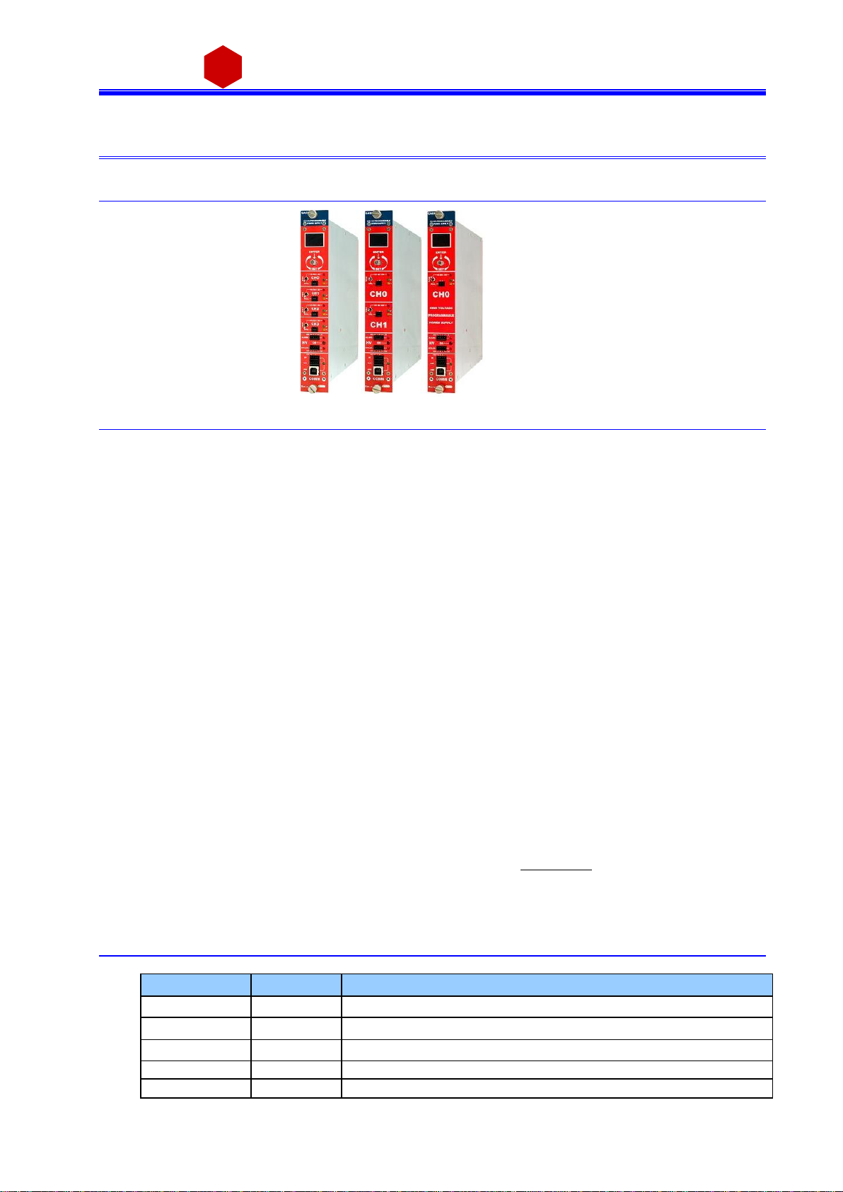
Fig.1.1: Mod. N1471 4 Channel Programmable HVPower Supply........................................................................................5
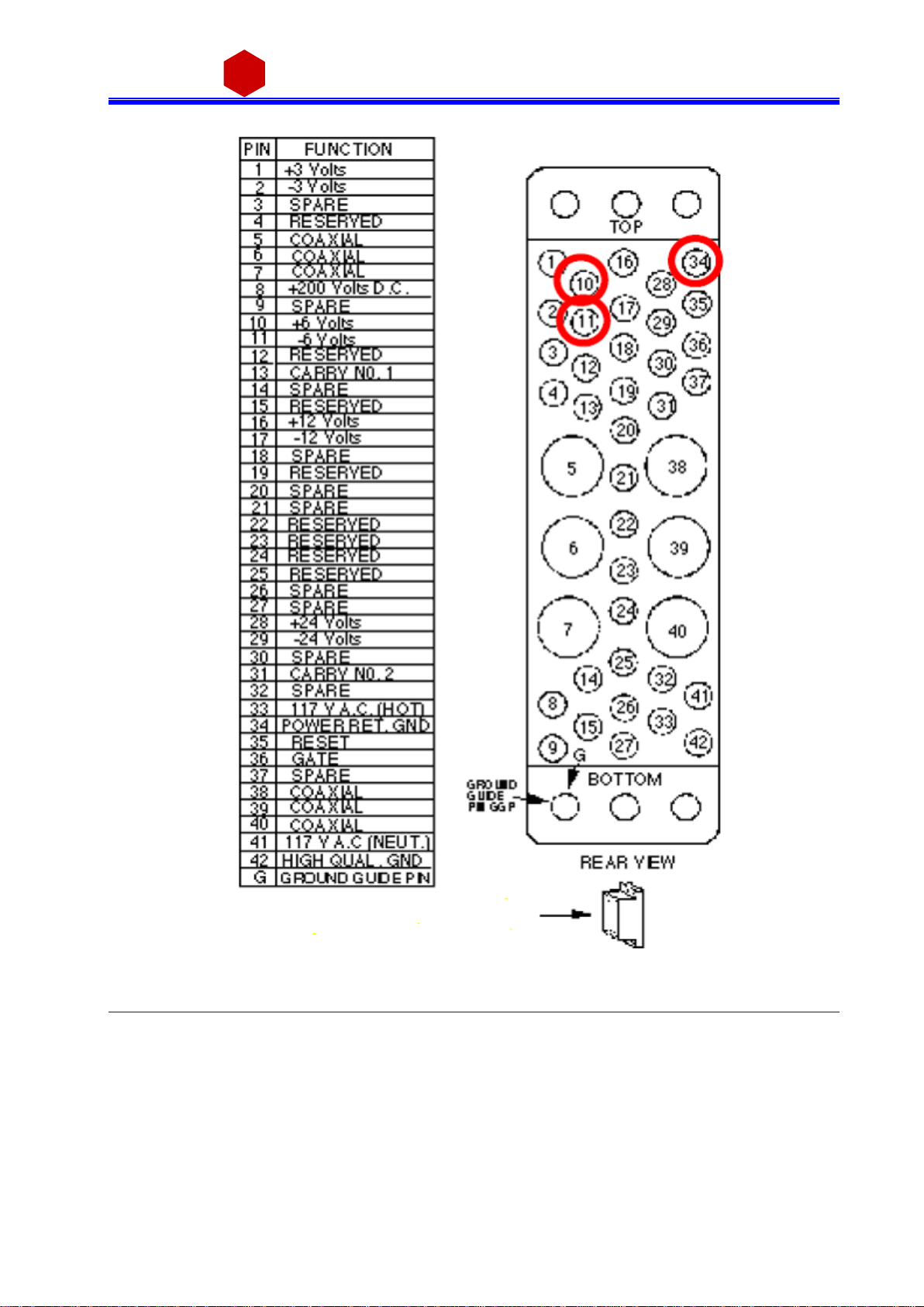
Fig. 2.1: Backplane NIMconnector................................................................................................................................................7
Fig. 2.2: Mod. N1471 series front panel (std, A, B, AL, AR) ......................................................................................................8
Fig. 2.3: Mod. N1471 series back panel (std., A, B) ...................................................................................................................9
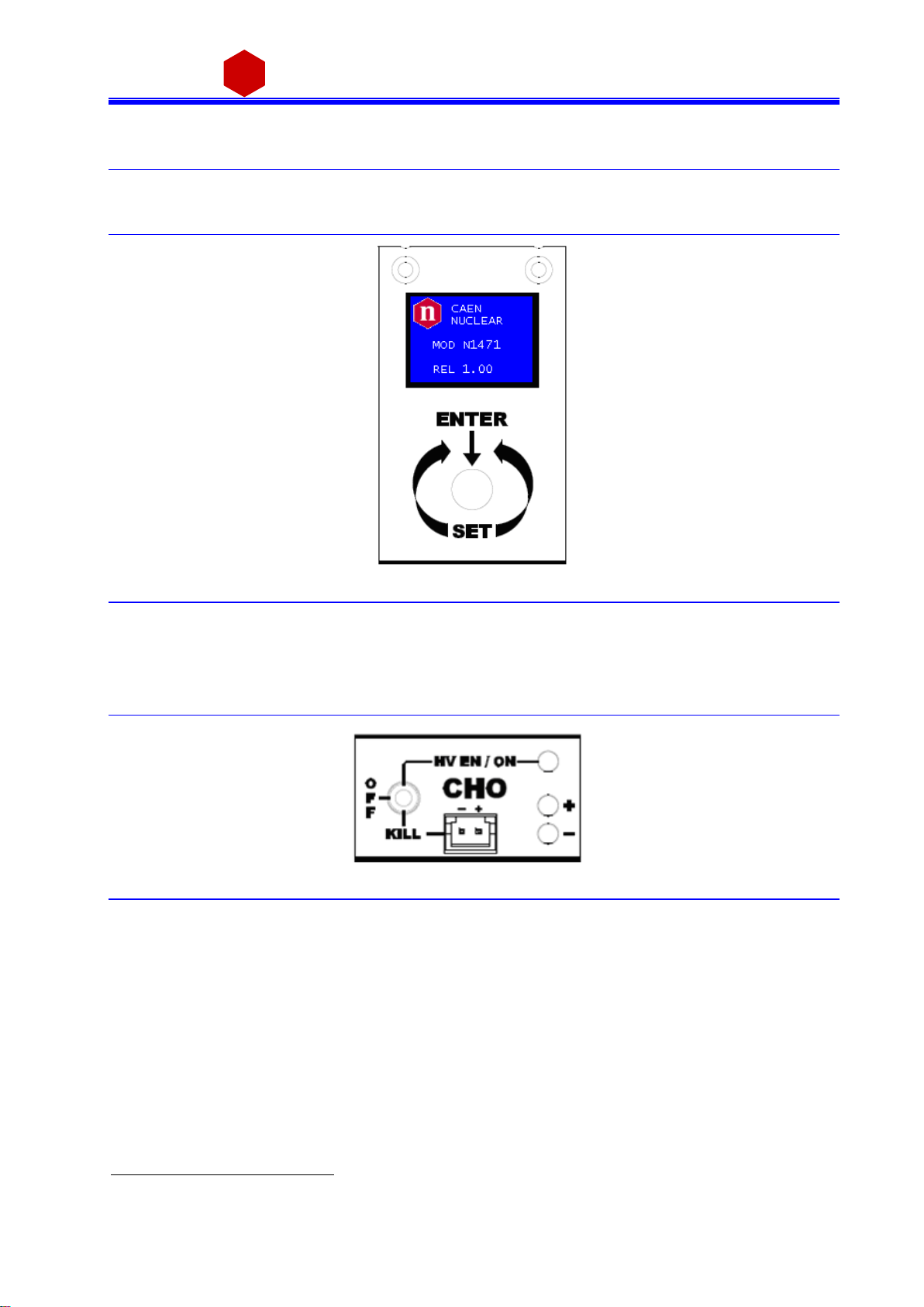
Fig.2.4: Local control panel.........................................................................................................................................................10
Fig. 2.5: Channel control panel and Kill scheme......................................................................................................................10
Fig. 2.6: N1471 HVStatus control panel...................................................................................................................................11

Programmable HV Power Supply
Revision19
4
n
CAEN
Tools for Discovery
Fig. 2.7: N1470 ALARMelectrical scheme................................................................................................................................11
Fig. 2.8: N1470 ALARMTTL configured....................................................................................................................................11
Fig. 2.9: N1470 INTERLOCK electricalscheme.......................................................................................................................11
Fig.2.10: Remote communication control and RS485 I/O –RS232 IN electricalscheme................................................12
Fig. 2.11: HVChannel panel and test point electrical scheme...............................................................................................13
Fig. 3.1: Welcomescreen.............................................................................................................................................................17
Fig. 3.2: Channel OFF status screen.........................................................................................................................................17
Fig. 3.3: Channel ON status screen...........................................................................................................................................17
Fig. 3.4: Channel KILL status screen.........................................................................................................................................18
Fig. 3.5: Mode settings status screen.........................................................................................................................................18
Fig. 3.6: Mode settings access screen.......................................................................................................................................18
Fig. 3.7: Mode settings editscreen.............................................................................................................................................18
Fig. 3.8: Channel settings editscreen........................................................................................................................................19
Fig. 3.9: Channel VSET select screen.......................................................................................................................................19
Fig. 3.10: Channel VSET access screen...................................................................................................................................19
Fig. 3.11: Channel VSET digit selectionscreen.......................................................................................................................19
Fig. 3.12: Channel VSET digit access screen...........................................................................................................................20
Fig. 3.13: Channel VSET digit adjust screen............................................................................................................................20
Fig. 3.14: Channel VSET digit confirm screen..........................................................................................................................20
Fig. 3.15: Channel VSET confirm screen..................................................................................................................................20
Fig. 3.16: Channel VSET de-selectscreen...............................................................................................................................21
Fig. 3.17: Channel KILL screen...................................................................................................................................................21
Fig. 3.18: Channel EXIT screen..................................................................................................................................................21
Fig. 3.19: Group selection............................................................................................................................................................22
Fig. 3.20: Group active..................................................................................................................................................................22
Fig. 3.21: Group VSET access screen.......................................................................................................................................22
Fig. 3.22: Group VSET digit selection screen...........................................................................................................................22
Fig. 3.23: Group Channel VSET digit access screen..............................................................................................................23
Fig. 3.24: Group VSET digit adjust screen................................................................................................................................23
Fig. 3.25: Group VSET digit confirm screen..............................................................................................................................23
Fig. 3.26: Channel VSET de-selectscreen...............................................................................................................................23
Fig. 3.27: Group EXIT screen......................................................................................................................................................24
Fig. 3.28: USB communication diagram ....................................................................................................................................25
Fig. 3.29: RS232 communication diagram ................................................................................................................................25
Fig. 3.30: RS485 communication diagram ................................................................................................................................26
Fig. 3.31: Ethernet communication diagram .............................................................................................................................26
Fig. 3.32: RS232 port cable adapter...........................................................................................................................................27
Fig. 3.33: Main Menu ....................................................................................................................................................................27
Fig. 3.34: Board Status Menu......................................................................................................................................................28
Fig. 3.35: Channels Menu............................................................................................................................................................28
Fig. 3.36: PC keyboard.................................................................................................................................................................28
Fig. 3.37: Channels group setting...............................................................................................................................................29
Fig. 3.38: Firmware Upgrade Menu/1.........................................................................................................................................29
Fig. 3.39: Firmware Upgrade Menu/2.........................................................................................................................................29
Fig. 3.40: Format EEPROM Menu..............................................................................................................................................30
Fig. 3.41: Current offset calibration warning.............................................................................................................................30
Fig. 3.42: Current offset calibration VSET selection................................................................................................................30
Fig. 3.43: Current offset calibration confirmation......................................................................................................................31
Fig. 4.1: Side cover removal instructions...................................................................................................................................35
Fig. 4.2: Polarityselection instructions.......................................................................................................................................36
Fig. 4.3: Dip switch position.........................................................................................................................................................37
Fig. 4.4: C21 jumper location.......................................................................................................................................................38
Fig.4.5: Earth configuration connection examples..................................................................................................................39
LIST OF TABLES
Table 1.1: Available items...............................................................................................................................................................5
Table 2.1: Power requirements......................................................................................................................................................6
Table 2.2: Interlock operation......................................................................................................................................................12
Table 2.3: Mod. N1471 Channel technical specifications .......................................................................................................14
Table 3.1: Smileys list...................................................................................................................................................................24

Programmable HV Power Supply
Revision19
5
n
CAEN
Tools for Discovery
1 General description
1.1 Overview
Fig. 1.1: Mod. ProgrammableHVPowerSupply
The Mod. N1471 provi des 4 independent High Voltage channels i n a single width NIM mechanics. Two a nd one
cha nnel versions (N1471A and N1471B) a re a ls o a vai lable.
Ea ch channel can provide a ±5.5kV / 300 µA ma x output.
Channels have common floating return (common return ins ul ated from the crate ground); HV outputs are
del ivered through SHV connectors.
The HV output RAMP-UP a nd RAMP-DOWN rates may be s electe d independently for each channel i n the range
1÷500 V/s i n 1 V/s steps .
Safety fea tures include:
• OVERVOLTAGE and UNDERVOLTAGE wa rning when the output volta ge di ffers from
the programmed value by more than 2% of s et va lue (mi ni mum 10V).
• Programmable VMAX protecti on l imi t
• OVERCURRENT detection: if a channel tries to draw a current larger than its programmed limit, it enters TRIP
status, keeping the maximum al lowed va lue for a programmable time (TRIP), before bei ng swi tched off
• Channels ca n be ena bl ed or di sabled indi vidua ll y through the Interlock logi c.
Modul e control can take place either locally, assisted by a Graphic color display (not available on Mod.N1471AR)
or remotely, via USB, RS232 or RS485 (not available on Mod.N1471AL); the RS485 port a llows to build a N1471s’
da is y chain network (up to 32 modules).
For remote operation,CAEN also provides GECO2020, a graphical application that allows to manage the N14xx
HV Power Suppl ies (a s wel l a s al l other CAEN Power Supplies ).
Moreover, these units ca n be managed via CAEN HV Wrapper, a set of ANSI C functions bundled in a l ibrary,
providing the software developer an unified software interface for the control of CAEN Power Supplies. This is a
low l evel a pplication in which the writing of the Control SW is assigned to the user. CAEN HV Wrapper is logically
located between an higher level applicati on, s uch as GECO2020, a nd the lower layer s oftwa re l ibraries . It
conta ins a generic s oftware i nterface independent by the Power Supply models a nd by the communica tion path
us ed to exchange data with them. For more info pl ease vis it: www.caen.it (products >firmwa re/softwa re
section).
The Mod. A1480 is a n opti ona l DC Input Power Equali zer which al lows to us e a different i nput power
dis tribution on the N147x modules .
Table 1.1: Available items
Code
Item
Description
WN1471X05AAC
N1471
4 Ch NIM Programmable HV Power Supply (±5.5kV, 300µA, 5nA res.)
WN1471A05AAC
N1471A
2 Ch NIM Programmable HV Power Supply (±5.5kV, 300µA, 5nA res.)
WN1471B05AAC
N1471B
1 Ch NIM Programmable HV Power Supply (±5.5kV, 300µA, 5nA res.)
WA1480XAAAAA
A1480
DC Power Input Equalizer for N147X Family
WPERS0147001
Customization
Imon Zoom x10

Programmable HV Power Supply
Revision19
6
n
CAEN
Tools for Discovery
2 Technical specifications
2.1 Packaging
The Mod. N1471 boa rds are hous ed in s i ngle wi dth NIM module s .
2.2 Power requirements
Table 2.1: Power requirements
Board type
N1471
Channel configuration
without A1480
with A1480
N° chON
Current (±12V)
Current (±6V)
n° chON
Current (±12V)
Current (±6V)
3kV/300µA
4 CH
860 mA
< 10mA
4 CH
750 mA
800 mA
5.5kV/30µA
4 CH
720 mA
< 10mA
4 CH
630 mA
600 mA
5.5kV/300µA
4 CH
1.02 A
< 10mA
4 CH
800 mA
900 mA
Board type
N1471A,N1471AL, N1471AR
Channel configuration
without A1480
with A1480
N° chON
Current (±12V)
Current (±6V)
n° chON
Current (±12V)
Current (±6V)
3kV/300µA
2 CH
620 mA
< 10mA
2 CH
500 mA
500 mA
5.5kV/30µA
2 CH
550 mA
< 10mA
2 CH
440 mA
400 mA
5.5kV/300µA
2 CH
700 mA
< 10mA
2 CH
530 mA
600 mA
Board type
N1471B
Channel configuration
without A1480
with A1480
N° chON
Current (±12V)
Current (±6V)
n° chON
Current (±12V)
Current (±6V)
3kV/300µA
1 CH
530 mA
< 10mA
1 CH
370 mA
400 mA
5.5kV/30µA
1 CH
470 mA
< 10mA
1 CH
340 mA
300 mA
5.5kV/300µA
1 CH
500 mA
< 10mA
1 CH
380 mA
400 mA
WARNING: i f the A1480 i s not i nstalled, ±6V power s upplies are required only by older versi ons of the N1471;
such boards can be recognized by the presence of power pins 10 a nd 11 on the backplane NIM connector (s ee
fi gure 2.1). If the A1480 is not instal led, new vers ions operate onl y wi th ±12V power supplies .

Programmable HV Power Supply
Revision19
7
n
CAEN
Tools for Discovery
Fig. 2.1: BackplaneNIMconnector

Programmable HV Power Supply
Revision19
8
n
CAEN
Tools for Discovery
2.3 Frontandbackpanel
Fig. 2.2: Mod. N1471seriesfront panel(std, A, B, AL, AR)

Programmable HV Power Supply
Revision19
9
n
CAEN
Tools for Discovery
Fig. 2.3: Mod. N1471seriesback panel (std.,A, B)

Programmable HV Power Supply
Revision19
10
n
CAEN
Tools for Discovery
2.4 Frontpanelconnections
2.4.1 Local control section1
Fig. 2.4: Localcontrol panel
NAME:
TYPE:
FUNCTION:
MONITOR
1” OLED DISPLAY (96x64)
Local settings monitoring
TUNE
ROTARY SWITCH
Parameter and Mode setting
2.4.2 Channel control section
Fig. 2.5: Channel control panel and Kill scheme
NAME:
TYPE:
FUNCTION:
HV_EN/OFF/KILL
3 POS. SWITCH
Channel Enable and turning OFF/KILL2
ON
RED LED
HV On enabled
REMOTE KILL
AMP 280370-2
The channel is KILLED either as the +/- contacts are open or as a
+4÷6Vdc voltage is fed to pin - (see note)
+
GREEN LED
Positive polarity
-
YELLOW LED
Negative polarity
1Not available on Mod. N1471AR
2OFF: Channel turned off according to RAMP DOWN setting; KILL: Channel turned off at fastest availabl e rate

Programmable HV Power Supply
Revision19
11
n
CAEN
Tools for Discovery
2.4.3 HV Status control section
Fig. 2.6: N1471HVStatus controlpanel
NAME:
TYPE:
SIGNAL:
FUNCTION:
ON
RED LED
HV On enabled (at least one channel ON)
ALARM
RED LED/ AMP 280371-2.
Out
Alarm status signaled (active LOW)
INTERLOCK
RED LED/ AMP 280371-2
In
Interlock signal
2.4.3.1 Alarm signal
Fig. 2.7: N1470ALARMelectricalscheme
As a n Al arm condition is detected (see § 3.5.3.1 a nd § 3.5.4.1) pi ns 2 a nd 3 (- and +) are closed; the conta ct can
be used to switch an external device s upplied by an external source, otherwise the VB a nd GND references can
be used to provide a TTL compati bl e l evel on pi n 2 a nd 3.
In the fi rst cas e (externally s uppl ied device) the ma ximum al lowed rati ngs are:
Maximum volta ge between + a nd -: 12V
Maximum s ink current a cross + and -: 100mA
In the l atter case, in order to produce a TTL compatible Alarm Out, pin 3 (+) must be connected with pin 4 (VB)
and pi n 1 (GND) with pin 2 (-); see the di agram bel ow:
Fig. 2.8: N1470ALARMTTL configured
2.4.3.2 Interlock signal
Fig. 2.9: N1470INTERLOCKelectricalscheme

Programmable HV Power Supply
Revision19
12
n
CAEN
Tools for Discovery
A s chematic diagram of the Interlock input is s hown in the figure above, where the diode is part of optocoupler
stage.
Interlock means that channels are hardware disabled. The interlock operati on i s expla ined by the following
table:
Table 2.2: Interlock operation
CONFIGURATION
INTERLOCK MODE (§ 3.1.1)
OPEN
CLOSE
leavecontactopen
INTERLOCK
ENABLED
voltagelevel (0÷1V,~5mA current)betweenpin2and pin 3
INTERLOCK
ENABLED
shortcircuitpin 1 withpin2, andpin 3 withpin 4
ENABLED
INTERLOCK
voltagelevel (4÷6V,~5mA current)betweenpin2and pin 3
ENABLED
INTERLOCK
The front panel Interlock LED is ON when the INTERLOCK i s enabled; as INTERLOCK is enabled, cha nnels are
turned off at the fa s test avai lable rate, regardl es s the RAMP DOWN s etting.
2.4.4 Remote communication control section3
Fig. 2.10: Remotecommunication controland RS485 I/O–RS232IN electrical scheme
NAME:
TYPE:
FUNCTION:
IN
AMP 280371-2
RS485 Input4; adaptable to RS232 standard
OUT
AMP 280371-2
RS485 Output
USB
B TYPE USB
USB2.0 compliant realized via USB ↔ RS232 FT232BM converter
3Not available onMod. N1471AL
4RS 485 Serial Port Interfaceallows tocontrolupto 32 modules connectedby atwistedpaircable;the firstandlastmodules must
be terminated, see§ 4.2.1.

Programmable HV Power Supply
Revision19
13
n
CAEN
Tools for Discovery
2.5 Rear panelconnections
2.5.1 HV Channel Output
Fig. 2.11: HV Channelpanel andtest point electrical scheme
NAME:
TYPE:
FUNCTION:
MON
AMP 280371-2
Vout/Iout Test point
OUT
SHV
HV Channel Output
The tes t points allow to monitor the ChannelOutput Voltage a nd Current according to the following conversion:
VMON: Vol tage l evel (1V = 1.5 kV ±1% rea dout; same polarity as cha nnel )
IMON high range: Volta ge level (1V = 66 µA ±3% readout; positive, 0÷5 V range )
IMON low range: Volta ge l evel (1V = 6.6 µA ±3% readout; positi ve, 0÷5 V range )
2.6 Imon Zoom
Imon Zoom is an optional feature that allows to monitor the channel current with an increased resolution (10x)
in the 0 –30 µA range; i f the Imon Zoomis i nstalled, by selecting Imon Range = LOW (see § 3.1.2), the output
current i s monitored with 0.5nA resolution (instead of 5 nA), in the 0 –30 µA range. It is i mportant to notice
tha t, if Imon Range = LOW i s s elected, and the channel draws a current larger than 30 µA, then Overcurrent i s
signa ll ed.

Programmable HV Power Supply
Revision19
14
n
CAEN
Tools for Discovery
2.7 Technicalspecificationstable
Table 2.3: Mod. N1471Channeltechnical specifications
Output channels:
Positive or Negative Polarity (requires internal setting, see § 4.1)
Output ranges:
5.5kV / 300µA
Max. Ch. Output Power:
1.65W
Vset / Vmon Resolution:
100 mV
Iset / Imon Resolution 5:
If IMON RANGE = High is selected resolution is 5 nA
If IMON RANGE = Low is selected resolution is 0.5 nA
Vmax:
0 ÷ 5600 V
Absolute maximum HV level that the channel is allowed to reach, independently from the preset value
Vset. Output voltage cannot exceed the preset value Vmax. The accuracy is 1 % ± 5 V
Vmax resolution:
± 1 V
Alarm output:
Open collector, 100 mA maximum sink current
Interlock input:
LOW: <1V; current~5mA; HIGH: 4÷6 V
Ramp Up/Down:
1÷500 Volt/s, 1 Volt/s step
Trip:
Max. time an "overcurrent" is allowedto last (seconds). A channel in "overcurrent" works as a current
generator; output voltage varies in order to keep the output current lower than the programmed
value. "Overcurrent" lasting more than set value (1 to 9999) causes the channel to "trip". Output
voltage will drop to zero either at the Ramp-down rate or at the fastest available rate, depending on
Power Down setting; in both cases the cha nnel is put in the OFF s tate. If trip= INFINITE, "overcurrent"
lasts indefinitely.
TRIP range: 0 ÷ 999.9 s; 1000 s = Infinite. Step = 0.1 s
Vmon vs. Vout Accuracy: 6
±0.02% of read value ±2V
Vset vs. Vmon Accuracy: 4
±0.02% of read value ±2V
Imon vs. Iout Accuracy: 4
If IMON RANGE = High: ±2% of read value ±20nA
If IMON RANGE = Low:±2% of read value ±2nA
Iset vs. Imon Accuracy: 4
If IMON RANGE = High: ±2% of read value ±30nA
If IMON RANGE = Low:±2% of read value ±3nA
Voltage
Ripple:7
typical
<5mVpp
maximum
<10mVpp
Humidity range:
0 ÷ 80%
Operating temperature:
0 ÷ 45°C
Storage temperature:
-10 ÷ 70°C
Vout / Temperature coefficient:
max. 50ppm / °C
Imon / Temperature coefficient:
max 100ppm/C°; max 300ppm/C° with Imon X10 zoom (optional)
Long term stability Vout vs. Vset:
± 0.02% (after one week @ constant temperature)
5The module is calibrated byintroducing a positive offset on the current monitor, see details in § 3.3
6From 10%to 90%of Full Scale Range
7Measuredwith:1mcable length; 2nF capacitance

Programmable HV Power Supply
Revision19
15
n
CAEN
Tools for Discovery
3 Operating modes
CAUTION: N1471 MUST BE USED ONLY IN CRATES WITH FORCED COOLING AIR FLOW!
Modul e control can take place ei ther local ly, or remotel y, via USB or RS485 (see § 3.4).
3.1 Programmableparameters
3.1.1 Boards parameters
General board parameters (CONTROL ca n be operated both in LOCAL a nd REMOTE mode; other moni tor and
settings a re all owed in LOCAL mode onl y; s ee § 3.2) i nclude:
Parameter:
Function:
Display:
Power
(Monitor)
Modul e power supply status
Termination
(Monitor)
Local Bus termination status (ON/OFF)
HV Cl ock
(Monitor)
Sync clock frequency (200±10 kHz correct value)
Local Bus
Baud Rate
(Monitor/Set)
9600, 19200. 38400, 57600, 115200 Baud
Local Bus
Address
(Monitor/Set)
Local Bus address for remote communication (0÷31)
USB Ba ud
Rate
(Monitor/Set)
9600, 19200, 38400, 57600, 115200 Baud
INTERLOCK
(Monitor/Set)
CLOSED / OPEN OPERATION (see § 2.4.3.2)
CONTROL
(Monitor/Set)
REMOTE: the module is controlled remotely; local monitor is allowed;
LOCAL/REMOTE s wi tch is enabled
LOCAL: the module is controlled locally; remote monitor is allowed

Programmable HV Power Supply
Revision19
16
n
CAEN
Tools for Discovery
3.1.2 Channel settings
For ea ch channel the following parameters ca n be programmed a nd monitored either locally or remotely (see §
3.4):
Parameter:
Function:
Unit:
Display:
Vmon
High Voltage Monitored value
Volt
Imon
Current Monitored value
µA
Vset
High Voltage programmed value
Volt
Iset
Current Limit programmed value
µA
MaxV
Abs olute maxi mum High Vol tage l evel tha t the
cha nnel is a ll owed to rea ch (s ee § 2.7)
V
Ramp-Up
Maximum High Voltage i ncrease rate
V/s
Ramp-Down
Maximum High Voltage decrease rate
V/s
Power Down
Power Down mode after channel TRIP
KILL or RAMP
Trip
Maximum ti me an "overcurrent" is allowed to last
expressed in s econds (see § 2.7)
s
Imon Ra nge
Current Moni tor Zoom 10x (optional)
H or L

Programmable HV Power Supply
Revision19
17
n
CAEN
Tools for Discovery
3.2 LocalControl
Ins ert the unit inside a powered NIM crate, and s witch it ON. At the power the Display shows for a few seconds
the fol lowing s creen.
Fig. 3.1: Welcome screen
At this point the module is ready to be operated locally. The TUNE ROTARY SWITCH (see § 2.4) i s lit up as longas
Local Control is enabled.
3.2.1 HV connection
Verify the channels polarity (polarity s etting is explained i n § 4.1) checking that the polari ty LEDs a re s wi tched
on a ccording to the programmed configuration (see § 2.4.1); verify the HV_EN/OFF/KILL 3 POS. SWITCH of each
cha nnel is s et to OFF; the Dis pl ay will show the fol lowing mess age i n the l eft l ower row:
Fig. 3.2: Channel OFF status screen
now connect the HV cable linking the outputs to the loads to b e supplied and enable the HV outputs swi tching
the HV_EN/OFF/KILL 3 POS. SWITCH i n the HV_EN position; the Display will show the following mess age i n the
left lower row:
Fig. 3.3: Channel ON status screen
The KILL position of the HV_EN/OFF/KILL 3 POS. SWITCH allows to turn off the module at the fastest avai lable
rate; the Dis pl ay will show the foll owi ng mess age i n the l eft l ower row:

Programmable HV Power Supply
Revision19
18
n
CAEN
Tools for Discovery
Fig. 3.4: Channel KILL statusscreen
3.2.2 Module settings
Modul e settings a re genera l boa rd setti ngs; turn the TUNE ROTARY SWITCH unti l this s creen is shown:
Fig. 3.5: Mode settings status screen
Push the TUNE ROTARY SWITCH i n order to access MODULE pa rameters ; the MODULE frame becomes red:
Fig. 3.6: Mode settings accessscreen
The TUNE ROTARY SWITCH allows to s el ect the pa rameter to be s et; turn the ROTARY SWITCH unti l s uch
pa rameter is displayed (for example CONTROL), then select it by pushing the ROTARY SWITCH (the parameter is
shown wi th a red frame as l ong as it is active):
Fig. 3.7: Mode settings editscreen
Select the desired value by turning the TUNE ROTARY SWITCH and confirm i t by pushing the s wi tch itself.

Programmable HV Power Supply
Revision19
19
n
CAEN
Tools for Discovery
3.2.3 Channel settings
In order to operate Output Channel s ettings:
Turn the TUNE ROTARY SWITCH untilthe channel number to be s et i s displayed i n the left upper row (for
example Cha nnel 0)
Push the TUNE ROTARY SWITCH: at this point the frame of the left upper row (channel number) becomes red
and the cha nnel is s el ected
Fig. 3.8: Channelsettingseditscreen
Turn the TUNE ROTARY SWITCH untilthe parameter to be set (for example VSET) is displayed in the right l ower
row
Fig. 3.9: ChannelVSETselectscreen
Push the TUNE ROTARY SWITCH: a t this point the parameter is selected, i ts frame is shown in red and its na me
in bl ue; i t i s now possi bl e to cha nge the pa rameters va lue
Fig. 3.10: ChannelVSETaccess screen
Turn the TUNE ROTARY SWITCH untilthe value digit to be edi ted i s shown i n blue, the parameter name i n
yel low
Fig. 3.11: ChannelVSETdigitselectionscreen

Programmable HV Power Supply
Revision19
20
n
CAEN
Tools for Discovery
Push the TUNE ROTARY SWITCH: at this point the val ue digi t becomes yel low and can be edited
Fig. 3.12: ChannelVSETdigitaccess screen
Turn the TUNE ROTARY SWITCH until the digi t reaches the des ired val ue
Fig. 3.13: ChannelVSETdigitadjust screen
Confirm it by pus hi ng the TUNE ROTARY SWITCH, the edi ted digi t returns blue
Fig. 3.14: ChannelVSETdigitconfirm screen
Once a ll the digits a re set to the desi red va lue, turn the TUNE ROTARY SWITCH until the para meter name
returns bl ue
Fig. 3.15: ChannelVSET confirm screen
Push the TUNE ROTARY SWITCH in order to de -s el ect the pa rameter, the frame returns to bl ue
Other manuals for N1471 Series
1
This manual suits for next models
8
Table of contents
Other Caen Power Supply manuals

Caen
Caen SY 2527 User manual

Caen
Caen A3486 Technical document

Caen
Caen N1471 Series Technical document

Caen
Caen DT54 Series User manual

Caen
Caen A1536 User manual

Caen
Caen DT5519EN User manual

Caen
Caen A 1732 Technical document

Caen
Caen EASY3000 Technical document

Caen
Caen N471A Technical document

Caen
Caen A7502 User manual