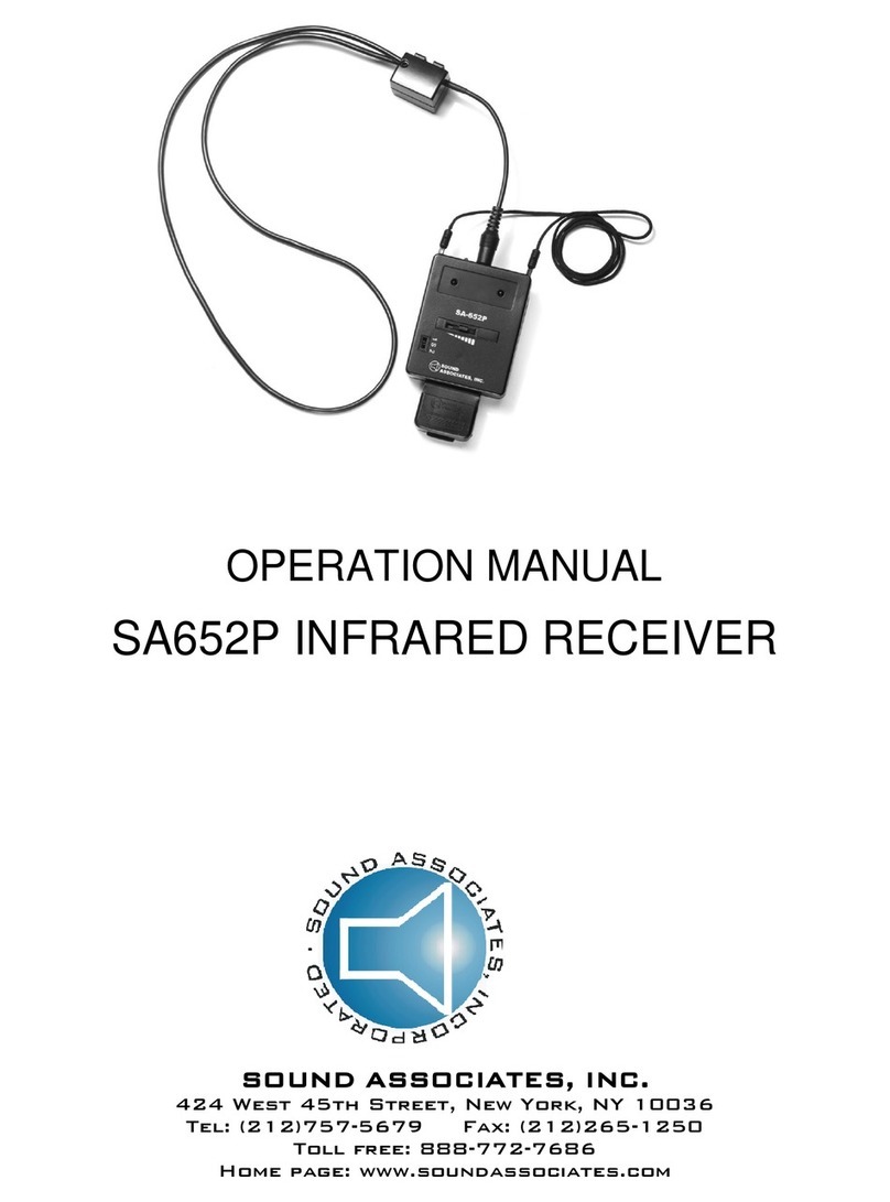
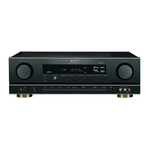
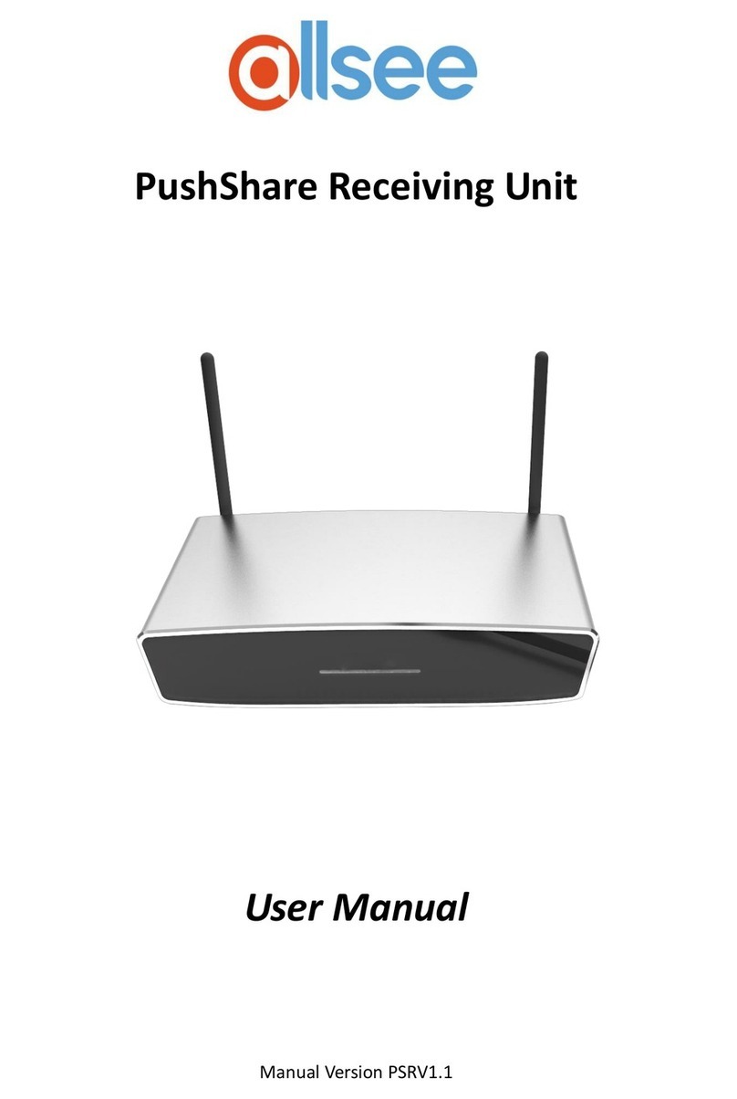
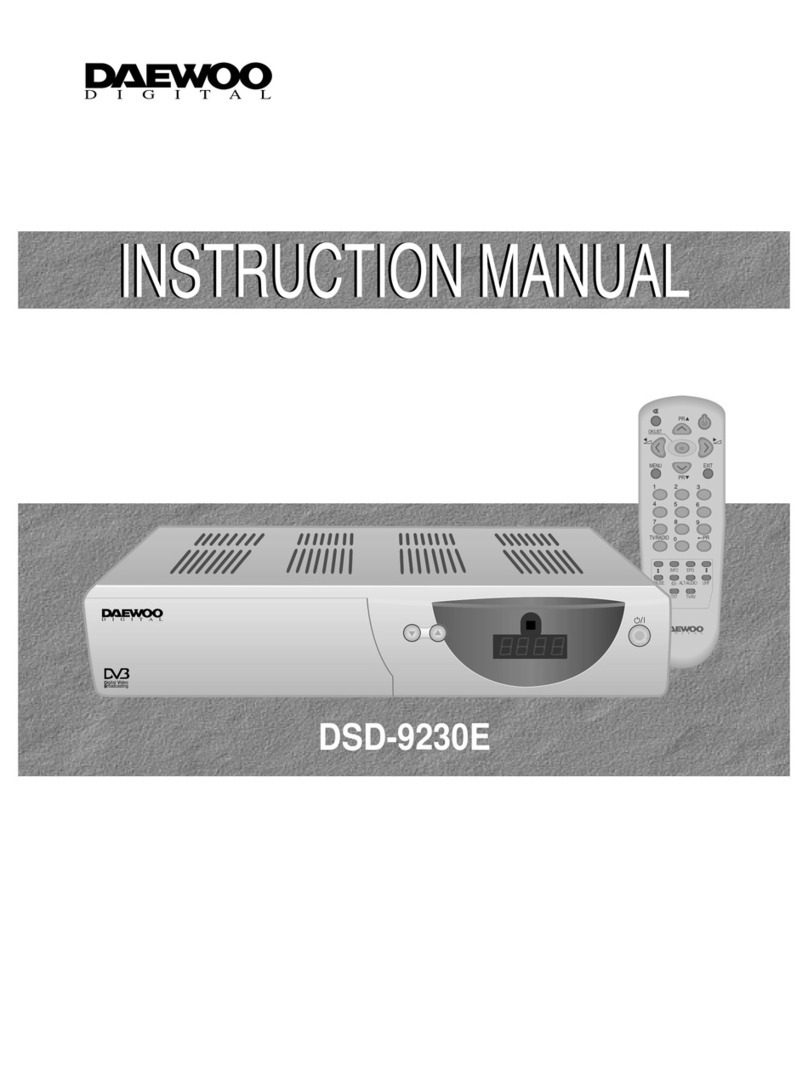
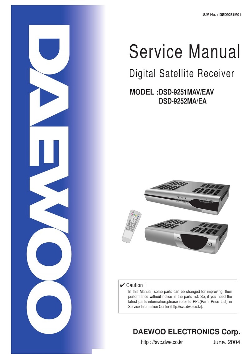
Daewoo DSD-9251MA User manual

Broadcasting
Digital VVideo
DSD-9251MADSD-9251MA
D I G I T A L
Digital Satellite Receiver
CHASSIS : SD-240V
Model :
DSD-9251MA
OCT 2003
S/M No : DSD240VEF0

1
GENERAL INFORMATION
1. General Information 2
2. Main Feature of DSD-9251MA 2
3. For Your Safety 2
4. Unpa king 2
5. General Operation of DSD-9251MA 2
6. About the Smart Card and CA Module 3
7. Remote Control 3
8. Front Panel 4
9. Rear Panel 4
10.Produ t Spe ifi ation 5
CIRCUIT OPERATING MANUAL
1. Blo k Diagram 6
2. Interfa e 7
3. Peripheral devi e of STI 5518 10
4. Front-End Interfa e 17
5. A/V Interfa e 20
6. Software Operating Steps 25
FIXING ERRORS
1. BOOTING ERROR 28
2. Disabled S reen 30
3. Faults in AUDIO/VIDEO system 33
PART LIST 35
SCHEMATIC DIAGRAM 39
EXPLODED VIEW 51

2
GENERAL INFORMATION
1 GENERAL INFORMATION
A Digital Satellite Re eiver is a onvenient produ t that allows you to view a variety of programs provided through satellite.
This user s guide overs the installation of the DSR and the ne essary steps to implement various features.
This also explains spe ial features available only in this DSR in detail, whi h will allow you to make full of these feature.
2 Main Feature of DSD-9251MA
¥ High quality Digital Video & Audio
¥ Fully MPEG2, DVB ompliant
¥ One step dire t move menu system (Go To fun tion)
¥ Provide friendly and easy-to-use menu system
¥ Install Wizard system in the earliest of the world
¥ Various hannel editing fun tion
(favorite, moving, lo king, renaming, deleting and sorting)
¥ User programmable various Satellite & Transponder information
¥ Automati ally sear h for newly added transponder
¥ Stores up to 2000 hannels
¥ Easy and speedy software upgrade through RS-232 port
¥ Plug-and-plug data transfer system (DSR to DSR)
¥ Automati ally ea h hannel volume saving fun tion
¥ Timer fun tion, automati ally turns On/Off by setting fun tion
(daily, weekly, monthly, one time)
¥ Automati reserved hannel moving system
¥ Provide Ele troni Program Guide (EPG)
¥ Teletext fun tion support
¥ Antenna Positioning Help feature
¥ Sele table Video output (CVBS, RGB)
¥ Provide various swit h types, LNB types and NTSC/PAL monitor type
¥ SCPC/MCPC Re eivable from C/Ku Band Satellite
¥ Multi LNB ontrolled by DiSEqC 1.0 DiSEqC 1.2 and 22KHz swit hing
¥ 256 olors On-S reen-Display
¥ PAL&NTSC Video Compatible (TV Type auto dete t)
¥ Last hannel auto saving
¥ 2 CI Module Slot
3 For Your Safety
¥ Allow lear spa e around the DSD-9251MA for suffi ient ventilation
¥ Do not over the DSD-9251MA or pla e it on a unit that emits heat
¥ Use a soft loth and a mild solution of washing-up liquid to lean the asing
¥ Do not onne t or modify ables when the DSD-9251MA is plugged in.
¥ Do not remove the over
¥ Do not allow the unit to be exposed to hot, old or humid onditions
¥ Never allow liquids, spray or other materials to ome into onta t with the inside of the DSD-9251MA
4 Unpacking
After pur hasing the DSR, unpa k it and he k to make sure that all of the following items are in luded in the pa kaging
¥ 1 x Remote Control Unit (RCU)
¥ 1 x User s Guide
¥ 1 x DSR
5 General Operation of DSD-9251MA
Throughout this manual you will noti e that the everyday operation of your DSD-9251MA is based on a series of user
friendly on s reen display and menus. These menus will help you get the most from your DSD-9251MA, guiding you
through installation, hannel organizing, viewing and many other fun tions.
All fun tion an be arried out using the buttons on the remote ontrol, and some of the fun tion an also be arried out
using the buttons on the front panel.
3
General Information
If at any time when you using the menus you want to return to the normal TV mode, press the TV/AV button.
The DSD-9251MA Mis easy to use, always at your ommand and adaptable for future advan es.
Please be aware that new software may hange the fun tionality of the DSD-9251MA
Should you experien e and diffi ulties with the operation of your DSD-9251MA, please onsult the relevant se tion of
this manual, in luding the Problem Shooting, or alternatively all your dealer or a ustomer servi e adviser.
PR
PR
PR
OK/LIST
MENU
TV/RADIO
EXIT
PAUSE
TXT TV/AV
L
R
INFO EPG
UHF
ALT-AUDIO
Key Function
Swit hes between the operational mode and stand-by
mode of the re eiver (Green lamp lights up during the
operation, Red lamp lights up in stand-by mode)
TV/ RADIO Swit hes between TV and Radio mode.
Mutes the sound.
Swit hes ba k to previous hannel.
INFO Shows information of the urrent hannel.
MENU Displays menu on s reen, and alls ommand box.
EXIT Returns to the previous menu on the menu s reen.
ALT-AUDIO
When wat hing a hannel, swit hes the audio
languages.
EPG Calls up the EPG
(Ele troni Program Guide)
OK/LIST Exe utes the sele ted item in the menu s reen, or
enters the desired value in any input mode.
0 - 9 Enter the number in the required menu item or sele t
a hannel number to wat h.
PR When wat hing, hanges hannels, or moves to the
next higher or lower item in the menu.
When wat hing, adjusts the volume, or moves to the
left or right item in menu.
Moves up / down a page in the hannel list.
PAUSE Press on e to freeze the s reen pi ture.
Press on e again to go to the normal mode.
Sele ts the different audio model.
TXT Swit hes to the Teletext mode.
UHF Swit hes to the UHF Tuning Mode.
TV/AV Swit hes between TV and AV mode.
L
R
PR
7 Remote Control
6 About the Smart Card and CA Module
To be able to re eive s rambled digital satellite hannels you will need a
Common Interfa e CA(Conditional A ess)module and a smart ard from a
Servi e Provider. It is possible to use two CA modules. The Servi e Provider is
the programme distributor. The Servide Provider is the programme distributor. If
you are subs ribing to servides from more than one Servide Provider, you might
have to hange between different Smart- ards and/or CA modules. Please note
that a Smart ard and CA module may only be valid for a single Servi e Provider
and due to this, a spe ifi range of hannels. The Smart ard and the CA module
may also provide a ess to spea ial menus not des ribed in this manual. If so,
please follow the instru tions from the Servide Provider. Only free to air
hannels are available without the Smart ard and/or the CA Module.
Note : The Smart ard and/or the CA module are distributed by your Servi e
Provider. After inserting the ard, leave it in the solt permanently. Do not remove
it again, unless your Servi e Provider asks you to do so. This is important,
be ause if your Servide Provider wants to download new information to the
Smart ard, the ard has to be in the slot.

4
General Information
8 Front Panel
9 Rear Panel
KEY FUNCTION
Swit hes between the operational mode and stand-by
mode.
When wat hing, hanges the hannel, or in the menu,
moves to the previous and next item.
Broadcasting
Digital V
V
ideo
DSD-9251MA
DSD-9251MA
D I G I T A L
CAUTION
90-250V~
50/60Hz, 30W
VIDEO
R
_
AUDIO
L
_
AUDIO
LNB IN
LNB OUT
_
RS 232
TV
13/18V
Max. 500mA
CONNECT TO TV AND
RS232 : CONNECT TO A PC FOR S/W UPGRADE
LNB IN : CONNECT TO SATELLITE ANTENNA
LNB OUT : CONNECT TOANOTHER RECEIVER
CONNECT VIDEO TO ATV USING RCA JACK
CONNECTAUDIO L/R TO TV OR AUDIO TUNER
geprufte
Sicherheit
OFF
ON

5
General Information
10 Product Specification
System Capabilities : Fully DVB ompliant
Demodulator
Waveform : QPSK demodulation and FEC de oding in a ordan e with
DVB prETS 300 421
Symbol rate : 2 < Rs < 45 Msps
Video Decoder
De ompression : MPEG-2 Mian Profile@Main Level
Data rates : Up to 60 Mbits/s
Video formats : 4:3, 16:9
Audio Decoder
De ompression : MPEG laver I and II, Musi am
Outputs : Stereo Channel, Dual Mono, Joint Stereo, Mono
Application System Resources
Mi ropro essor : St Mi roele troni s STi5518
Clo k frequen y : 81 MHz
Flash memory : 1 Mbyte
SDRAM : 8 Mbyte
Graphi display : 720 x 576 (PAL)
720 x 480 (NTSC)
Connector Summary
LNB : 1 x LNB input (F-type)
: 1 x LNB output (F-type : Loop through) : Option
RCA : 4 x RCA ja ks (CVBS, Audio L/R)
SCART : 1 S art (TV)
RS232 : 1 x 9-pin D-sub (Max 625K bits/s)
LNB & Tuner Input
Input frequen y : 950 to 2150 MHz
Digital signal input level : -65 to -25 dBm
LNB supply : 13.0 0.5V / 18.0 0.7V, max.500mA
Band swit h ontrol : 22 KHz (Mi ropro essor ontrol)
Conne tor : 1 x F-Type, 3/8-32UNEF-2A
2 x F-Type, 3/8-32UNEF-2A (Option)
Power Supply
Main input voltage : 90 - 250V AC 50Hz/60Hz
Normal power onsumption : 30W
Remote Control
Number of keys : 31 Keys
Operating distan e : Up to 10m
Front Panel
Number of keys : 3 Keys
Indi ators : power on / Stand by
Display : 4 Digits (7 segments)
Remote ontrol input : Infrared re eiver

6
CIRCUIT OPERATING MANUAL
1 Block Diagram
DSD-9230E BLOCK DIAGRAM
DSD- 9251MA Block Diagram
CPU
(STi5518)
AUDIO D/A
FLASH ROM
(4Mbit)
SDRAM
(32Mbit)
Television
Satellite dish
TUNER
A/D
6bit
DUAL
LINK IC
QPSK
FEC
RCA
CON
TV
SCART
RCA
RS-232
PORT
AV
S/W
(MM1232)
VIDEO
AUDIO
FRONT
SMPS
+5V
+3.3V
+12V
+30V
+22V
+7.5V
Digital
Audio
Converte r
(TDA1315)
RCA
Interface
I
2
C BUS
POSITIONER
& SKEW
Feature 1. Blo k Diagram

7
CIRCUIT OPERATING MANUAL
2 Interface
(1) Key Interface
Input an be made by Key using PIO Port for the Key I/O ontrol.
The key value after the s anning is al ulated by one Input port and 7 Output Ports.
Output ports are used with the segments of the display.
* Key S an Method
Perform the Low S an ,using the Key Output Port(KO0-7) with the
y le of 64ms. If the Key is pressed, the Key Input Port will
re ognize the status as low eventually lead to the key ode value
while going through the step from K0 to K7.
S1
R1
10K S2 S3 S4 S5 S6 S7 S8
VCC
KI1
K0-K7
K0
K1
K2
K3
K4
K5
K6
K7
KI1
K7_SEG_CLK
K6_SEG_G
K5/SEG_F
K4/SEG_E
K3/SEG_D
K2/SEG_C
K1/SEG_B
K0/SEG_A
64ms
Feature 2. Key S an

8
CIRCUIT OPERATING MANUAL
(2) Remote controller Interface
Re ognize the REMOCON Code value after analyzing Interrupt Interval Time through PIO Port that reads the output
signal of the IR sensor.
MITSUBISH formats were used for the REMOCON signal. Following is the Timing Diagram for the MITSUBISH signal
format.
The signals are made up of Leader Code, Custom Code (8bit), Separator and Data Code (8bit). Following is the value
of the individual Key.
8.0 4
C
ustom co
d
e
8bit
D
ata
bi
t
8bit
60 60
60
8.0 4.0
0.5
0.5
0.5
1
.5
Feature 3. MITSUBISH Format Timing

9
CIRCUIT OPERATING MANUAL
Chart 1. Remote ontroller Key Code
Key Function Hex Key Function Hex
Custom ode 0x16 0x1C
Power 0x15 INF0 0x21
Mute 0x12 PR 0x17
1 0x01 PR 0x18
2 0x02 0x14
3 0x03 0x13
4 0x04 OK 0x11
5 0x05 EXIT 0x23
6 0x06 0x1D
7 0x07 EPG 0x24
8 0x08 PAUSE 0x1E
9 0x09 Audio-L/R 0x0D
0 0x00 ALT-AUDIO 0x0E
TV/RADIO 0x0A TXT 0x25
PR 0x20 UHF 0x26
MENU 0x22
(3) Display Interface
The signal that ontrols the Segment of 7-Segment is used with the signal of Key S an as mentioned above in Key
Interfa e se tion.
Common signals that ontrol Digit use PIO (PIO3-0,1,2,3 and 4)
Following pi ture shows the stru ture of operation. Display use Common Cathode Type. Display is a tivated by
re urrent signals with y le of 1~3ms.
3V3
E
Q1
B57
C
BR1
2.2K
COM0
2
1
C
D1 DX8
R2
33
Q2
B47
B
E
GND
R3
2.2K
SEG_A

10
CIRCUIT OPERATING MANUAL
3 Peripheral device of STI5518
(1) Stru ture
STI5518 is a 1 hip in luding 32bit RISC CPU, A/V Demux, Video En oder, Multi PIO and Ca he RAM for the use of
DVB and DSS Set Top.
Followings are summary of distin tive features of ea h Blo k.
Enhan ed apability with 32bit VL-RISC CPU Core of 81MHZ lo k.
Supporting Bandwidth of 200MB/S using internal 2KB SRAM buffer and 2KB DCACHE.
Video De oder is atta hed inside supported by MPEG-2 MP@ML and Letter Box.
MPEG Layer1 and 2 Audio De oder are stored inside.
Providing interfa e external AC3 De oder.
Supporting 2 - 8bit/pixel OSD.
Internally stored Video En oder for the output of RGB, CVBS and Y/C Video
Enhan ed CPU and De oder apability boosted by 64Mbit SDRAM.
Ba king External Surrounding Interfa e Memories. ( 4 Banks )
Able to use Hardware DMUX, input Serial and to support 32Pid.
Boosting 8 Level INT.
Supporting DMA and other multi PID.
2 MPEG
DMAs
Serial
IEEE 1394
Hardware
transport
strearn
demux
2 Kbytes
Instruction
cache
2K Data
cache and
2K SRAM
OS-Link
2 UART
1 I2C
PIO
3 PWM
Diagnostic
controller
and
systems
services
SDAV
interface
Block move
DMA
ST20
CPU
Interrupt
controller
EMI
2
SmartCard
interfaces
(ASC)
MPEG
audio
decoder
AC-3 I/F
MPEG
video
decoder
PAL/NTSC
Encoder
Teletest
interface
Feature 5. Sti5518 Blo k Diagram

11
CIRCUIT OPERATING MANUAL
(2) Reset Section
If the Low signal is read by Sti5518 Reset Pin, the Register value of all Sti5518 will be initialized.
There must be at least of 8 lo k (37nse ) of Reset Time.
(3) Clock Section
STI5518 has two PLL inside. Operative lo ks are made by external lo k with one unit of 27MHz. The two PLL are as
of ST20 PLL and MPEG PLL.
ST20 PLL produ es 81MHz of system lo k that is to be used in pro essor and peripheral equipment.
MPEG PLL produ es audio de oder system lo k, audio PCM lo k, TS Demultiplexer and memory lo k of SDRAM.
27MHz lo k uses VCXO. Curren y ontrol is enabled by PWM OF Sti5518 PWM with the referen e of the PCR
value of MPEG to set the exa t initiative of MPEG. If this value is not appropriate the olors are not be seen on the
s reen, or the s reen will display broken features.
(4) PIO Structure
Sti5518 supports PIO that ba k up 5 number of Ports (8bit) as of PIO0, PIO1, PIO2, PIO3 and PIO4. Some ports are
able to endow extra fun tions to PIO for flexible expansion in usage. Following hart shows Alternative Fun tion Pin of
PIO.
PIO port 0
ASC0TxD or
S 1DataOut
ASC0RxD or
S 1DataIn
Not onne ted
S 1Clk
(S 1RST)
(S 1CmdV )
ASC0Dir
(S 1Dete t)
PIO port 1
SSC0 MTSR
SSC0 MRST
SSC0 SCIK
CaptureIn1
CaptureIn2
ASC1TxD
ASC1RxD
ASC3TxD
PIO port 2
ASC2TxD
or S 0DataOut
ASC2RxD
or S 0DataIn
Not onne ted
S 0Clk
CompareOut0
(S 0RST)
(S 0CmdV )
Not onne ted
CaptureIn0
(S 0Dete t)
PIO port 3
TriggerIn
TriggerOut
PIO port 4
CompareOut1
(IROut)
CaptureIn3
ASC3RxD
not_Rst
tRSTLRSTH
Min 8x37nsec
Feature 6. Reset Timing
Chart 2. PIO Alternate Fun tions.
Alternative fun tion of PIO pins
Port bit
0
1
2
3
4
5
6
7

12
CIRCUIT OPERATING MANUAL
This se tion only provides summaries of individual fun tion of ea h Port.
Further dis ussion will be followed in individual port se tion.
¥I
2C_DATA (PIO1_0)
¥I
2C_CLK (PIO1_2)
Used for the transmission of Serial and ontrol of Tuner, CI-Max, AV Swit h and RF Modulator.
ClkPolarity ClkPhase
01
Serial clock SCIK
Plns MTSR/MRST
First
bit Last
bit
Shift data
Latch data
Transmit data
Feature 7. I2C Timing
Chart 3. PIO Map
PIO NAME I/O Function Remarks
PIO1_0 I2C_Data(SSC0) I/O
PIO1_2 I2C_Clk O
PIO1_3 NOTPGM_EN O L:Flash program enable
PIO1_4 SLOW_S/W I H:VCR S art Input ON
L: VCR S art Input OFF
PIO1_5 RS232_Tx O
PIO1_6 RS232_Rx I
PIO2_7 KI1 I
PIO3_0 COM0 O
PIO3_1 COM1 O
PIO3_2 COM2 O
PIO3_3 COM3 O
PIO3_4 COM4 O
PIO3_5 Seg_ lk/K7 O
PIO3_6 TriggerIN I
PIO3_7 TriggerOUT O
PIO4_0 SegA/K0 O
PIO4_1 SegB/K1 O
PIO4_2 SegC/K2 O
PIO4_3 SegD/K3 O
PIO4_4 SegE/K4 O
PIO4_5 SegF/K5 O
PIO4_6 REMOCON_IN I
PIO4_7 SegG/K6 O

13
CIRCUIT OPERATING MANUAL
¥ NOTPGM_EN (PIO1_3)
Flash ROM Write prote t/ Program enable (Low) or Program disable (High)
¥ SLOW_S/W (PIO1_4)
Che king the onne tion of external features with V r s art su h as VCR and general power on/off status. Conne t and
power on(High), Not onne t or power off(Low)
¥ RS232_Tx (PIO1_5)
¥ RS232_Rx (PIO1_6)
Rs232 serial data transfer (Used to S/W upgrade, Debugging)
¥ KI1 (PIO2_7)
Key input he k. Reading Keys when in the Low status.
¥ COM0 (PIO3_0)
¥ COM1 (PIO3_1)
¥ COM2 (PIO3_2)
¥ COM3 (PIO3_3)
¥ COM4 (PIO3_4)
Sele ting 4 Digit of the Display, in luding lo k dots. If it s in Los status, the Digit will be in ON status.
SegA/K0 (PIO4_0)
¥ SegB/K1 (PIO4_1)
¥ SegC/K2 (PIO4_2)
¥ SegD/K3 (PIO4_3)
¥ SegE/K4 (PIO4_4)
¥ SegF/K5 (PIO4_5)
¥ SegG/K6 (PIO4_7)
¥ Seg_ lk/K7 (PIO3_5)
Signals the segment of Display and Dot (is ON when in High status) and Key S an.
¥ Trigger IN (PIO3_6)
¥ Trigger OUT (PIO3_7)
Used when debugging with DCU Tool
REMOCON_IN (PIO4_6)
Re ognize the REMOCON signal being sent from IR Sensor.
(5) Memory Interface
Sti5518 an support both On- hip memories that are 2KB SRAM, 2KB SRAM or Data Ca he and 2KB Instru tion
Ca he and external expanded memories as of ROM and DRAM. Moreover, SDRAM an be used up to 32Mbits with
MPEG memory. From the 32Mbits SDRAM 16Mbits an be used as the buffer of MPEG and the rest of 16Mbits an be
used as Code buffer enabled by Code on SDRAM program.
A. REGION 0
On-Chip memory, Handler, Trap and DMA are allotted from the address 0X80000000 to 0XBFFFFFFF.
B. REGION 1
From the address 0XC0000000 to 0XC0400000 are used as a buffer memory of MPEG.
C. REGION 2
From the address 0X00000000 to 0X3FFFFFFF, they re used for the surrounding area for the internal parts. Individual
part has 4Kbyte.
D. REGION 3
EMI (Extended Memory) is divided to 4 Banks. Bank 0 is only appli able for the DRAM Interfa e.

14
CIRCUIT OPERATING MANUAL
Following is the Memory MAP Table.
EMI Bank 3 (FLASH)
EMI Bank 2
EMI Bank 1
EMI Bank 0
Shared SDRAM
Peripheral configuration registers
Reglon 3Reglon 2Reglon 1Reglon 0
0x70000000
0x7FFFFFFF
0x60000000
0x50000000
0x40000000
0x20040000
0x00000000
0xC0000000
0x80000800
MinInt: 0x80000000
0x80001000
0xC0400000
Not available
2 Kbyte data cache when used as SRAM
2 Kbyte SRAM
Not available
Feature 8. Memory Map
The size of EMI Bus is 16bit and also support for the 8bit Bus. The Bank0 of EMI an support DRAM Interfa e while rest of
Bank as of Bank1, 2 and 3 an only support SRAM, ROM and Peripheral Interfa e.
¥ Data 0 - 15
16bit data transfer
¥ Adr 1 - 21
When using DRAM, it supports Multiplex mode (Row and Column Address) with the a ess ability of 32bit.
¥ not_WE0
¥ not_WE1
Signals individual bite Enable Strobe when addressing 2bit word at EMI.
Not_WE0 assert : Data 0 - 7 enable
Not_WE1 assert : Data 8 - 15 enable
¥ not_CE0
¥ not_CE1
¥ not_CE2
¥ not_CE3
EMI Bank0/1/2/3 Chip sele t strobe

15
CIRCUIT OPERATING MANUAL
¥ MemWait
Wait signal is produ ed in external devi e when a essing SRAM and peripheral devi es. Wait signal is maintained as
Order status in the High status motivated by pro essor lo k.
¥ Not_OE
Read Strobe
¥ ReadnotWrite
The ability to Read or Write of pro essing y le.
A ess y le of EMI Bank3 and Bank2 is as following feature. The value of timing hart an be modified by the value of
Configuration Register setting.
Symbol Parameter Min Max Units Note
tCHAV Refere ne Clo k high to Address valid -8.0 0.0 ns
tCLSV Referen e Clo k low to Strobe valid -8.0 3.0 ns
tCHSV Referen e Clo k high to Strobe Valid -8.0 0.0 ns
tRCA/CH Read Data valid to Referen e Clo k high 13.0 ns
tCHRDX Read Data hold after Referen e Clo k high -2.0 ns
tSVRDX Read Data hold after Strobe valid 0.0 ns 1
tCLWOV Referen e Clo k low to Write Data valid -8.0 7.0 ns 1
tCHWOV Referen e Clo k high to Write Data valid -8.0 6.0 ns 1
tCHWDZ Referen e Clo k high to Write data tristate -8.0 6.0 ns
tCHRSV Referen e Clo k high to remaining Strobes valid -8.0 3.0 ns
tCHPH Referen e Clo k high to ProcClkOut high -8.0 0.0 ns
tWVCH MemWait valid to Referen e Clo k high 13.0 ns
tRVCH MemReq valid to Referen e Clo k high 13.0 ns
tRHWX MemWait hold after ProcClkOut high 0.0 ns 1
tPHRX Memreq hold after Pro ClkOut high 0.0 ns 1
tPHEMIZ MemGrant to signals tristate when bus granted TBD ns 1
Chart 4. EMI Timing Value

16
CIRCUIT OPERATING MANUAL
Feature 9. EMI Interfa e Timing

17
CIRCUIT OPERATING MANUAL
4 Front-End Interface
(1) Tuner Module
Tuner and QPSK Demodulator are ombined into one Module. Following feature shows the Blo k Diagram.
RFINPUTA
950 ~2150
VDD
(+3.3V) NRES SDA SCLB3
(5V)
AMP
RFATT
BPF
AMP
QPSK Link IC
STV0299B
SDAT
Loop
Through
Output
950 ~2150
B2
(5V)
ZERO IC
with
PLL
TUN
(30V)
B1
(5V)
SCLT
DATA[0:7]
STROUT
ERROR
CLK_OUT
D/P
AUX_CLK
BPF
LNB
Power B
LNB
Power A
T/M A/S
LPF
F22/DiSEqC
B4
(5V)
I
Q
AGC
CIRCUIT
Feature 10. Tuner Modul Blo k

18
CIRCUIT OPERATING MANUAL
* The fun tions of individual Pin.
PIN NAME PIN No PIN DESCRIPTION
LNB POWER B 1 LNB Voltage supply. To put 1000PF of erami apa itor into ground.
LNB POWER A 2 LNB Voltage supply. To put 1000PF of erami apa itor into ground.
A-GND 3,6 GND. Please don t let any Digital Noise enter through ground.
B1 4 5V Supply for RF Amp TR
B2 5 5V Supply for ZERO-IF hip(for RF)
B3 6 5V Supply for ZERO-IF hip(for PLL)
A/S 8 I
2
C Bus Address sele tion input (See table 3)
T/M 9 Tuning voltage monitor (Do not onne t it to anywhere)
TUNING(+30V) 10 PLL hannel sele t voltage supply (+30V)
B4 11 5V supply for AGC pull-up
NRES 12 Reset, a tive at low level.
AUX_CLK 13 Programmable Output Port or Programmable Output Clo k
F22/DiSEqC 14 DiSEqC modulation (22kHz Tone), Programmable Output Port
SCL 15 I
2
C Bus
SDA 17
N.C 16 Do not onne t it to anywhere
BCLK OUT 18 Output Byte Clo k; or Bit Clo k in Serial Mode.
N.C 19 Do not onne t it to anywhere
DO,....,D7 20~27 Output Data : D7 is DATA_OUT in Serial Mode.
N.C 28 Do not onne t it to anywhere
D/P 29 Data/Parity Signal.
ERROR 30 Output Error Signal. Set in ase of un orre table pa ket.
STR OUT 31 Output 1st byte Signal (syn hro byte lo k)
VDD 32 +3.3V Supply for LINK IC
Chart 5. Tuner Module Pin Out
Data
Parity
No Error
Uncorrectible Packet
No Error
BYTE CLK
PACKET
STR OUT
ERROR
BYTE DATA
Feature 11. Parallel Data Output Timing
TS Output is made by the Serial or Parallel fun tion.
The relationship between TS output Data and Control signal is showing in the following diagram. If an error o urs Data is
ignored, and the Data in the Valid area is valid.
Parallel Output Timing

19
CIRCUIT OPERATING MANUAL
START
Bit CL
K
PACKET
D7
ERROR
First bit of the packet
Data Parity
Parity
Useful Data
1 Packet
RS0 = 0
RS0 = 1
Feature 12. Serial Data Output Timing
Serial Output Timing
(2) Related with LNB
1) LNB power and 22khz Tone Pulse
The power supplied to LNB sends the 22Khz Tone signal that is used in horizontal(18V), verti al(13V) and frequen y
Band and Diseq Command.
UNI-CI Model uses LNBPIO series that are ex lusive IC for the LNB from ST ompany.
Control signal is sent through 74HC574(IC5and IC6) from CPU.
Chart 6. LNB Control signals
22KHZ Tone Spe is
Fun tion High Low
H/V Horizental(18v) Verti al (13v)
22Khz-ON 22Khz ON 22Khz OFF
LNB-ON LNB ON STD BY
AUX/IRD IRD MODE AUX MODE
(Loop Through) (External SAT)
Feature 13. 22Khz Tone Pulse
Table of contents
Other Daewoo Receiver manuals

Daewoo
Daewoo DSD-9280M User manual

Daewoo
Daewoo DSA-9310E User manual

Daewoo
Daewoo DSD-9251MAV User manual

Daewoo
Daewoo DSD-9230E User manual

Daewoo
Daewoo DCR-9130 SERIES User manual

Daewoo
Daewoo DSI-9300 User manual

Daewoo
Daewoo DSD-9250E User manual

Daewoo
Daewoo DSD-9502 Series User manual

Daewoo
Daewoo DR-C912B User manual

Daewoo
Daewoo DSI-9100 User manual