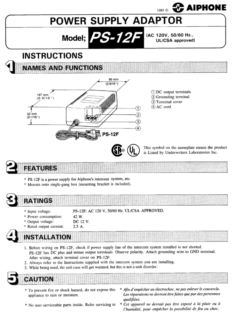
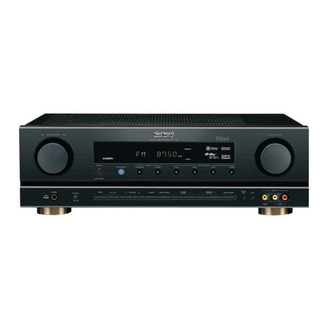
Daewoo DSD-9251MAV User manual

S/M No. : DSD9251M01
✔ Caution :
In this Manual, some parts can be changed for improving, their
performance without notice in the parts list. So, if you need the
latest parts information,please refer to PPL(Parts Price List) in
Service Information Center (http://svc.dwe.co.kr).
DAEWOO ELECTRONICS Corp.
June. 2004
http : //svc.dwe.co.kr
Service Manual
Digital Satellite Receiver
MODEL :
DSD-9251MAV/EAV
DSD-9252MA/EA

GENERAL INFORMATION............................................................................................2
CIRCUIT OPERATION MANUAL.............................................................................................7
FIXING ERRORS....................................................................................................................28
BOM LIST...............................................................................................................................33
SCHEMATIC DIAGRAM.........................................................................................................40
PARTS PLACEMENT(ARRANGEMENT)..............................................................................53
1
CONTENTS

2
GENERAL INFORMATION
Digital Satellite Receiver is easy to use, and allows you to watch digital programs broadcasted via satellite.
This instruction manual will guide you through the initial installation of your receiver.
It also describes how to take full advantage of a wide range of features that are easily accessible.
Read this instruction manual carefully before installing your receiver.
MAIN FEATURES
• High quality Digital Video & Audio
• Fully DVB compliant
• Common Interface with 2 PCMCIA slots
• User friendly and easy-to use menu system
• Various channel editing function, on Channel Management. (favorite, move, lock, rename, delete and sort)
• User programmable Satellite & Transponder information
• Automatic search for newly added transponder (NIT search)
• Stores up to 4000 channels
• Support software upgrading through RS-232C port
• Plug-and-play data transfer system (DSR to DSR)
• Individual channel volume saving function
• Timer function
• Automatic reserved channel moving system
• Electronic Program Guide (EPG)
• Teletext function support
• Support RGB and CVBS video output
• SCPC/MCPC receivable from C/Ku Band
• Multi LNB control by DiSEqC 1.0 and 22 KHz switching
• Motorized system control by DiSEqC 1.2* and USALS**.
• 256 color On-Screen-Display
• Support S/PDIF output
(Optional function)
* DiSEqC
TM
is a trademark of EUTELSAT.
** USALS
TM
is a trademark of Stab.
FOR YOUR SAFETY
•Allow clear space of more than 10 cm from the top, back and both sides for sufficient ventilation.
•Do not cover the Digital Satellite Receiver nor place it on a unit that emits heat.
•Use a soft cloth and a mild solution of washing liquid to clean the casing
•Do not connect or modify cables when Digital Satellite Receiver is plugged in.
•Do not remove the cover.
•Do not allow the unit to be exposed to extreme heat, cold or humidity.
•Never allow liquid spray or other materials to come into contact with the inside of the Digital Satellite Receiver.
•This Unit is designed for continuous operation. Switching it off does not disconnect it from the mains(Stand-by). To
disconnect it from the mains, you have to unplug the mains.
•The apparatus shall not be exposed to dripping or splashing and that no objects filled with liquids, such as vaseds,
shall be placed on the apparatus.
UNPACKING
1 x Remote Control Unit (RCU)
2 x AAA battery (option)
GENERAL OPERATION
Throughout this manual you will notice that the operation of your Digital Satellite Receiver is based on a series of user
friendly On Screen Display menus.
These menus will help you to get the most out of your Digital Satellite Receiver And guide you through installation.
All function can be carried out by using the keys on the remote control.
The Digital Satellite Receiver is easy to use, and adaptable for future upgrades.
Note that new software may change the functionality.
If you have difficulties with the operation of your Digital Satellite Receiver, please refer to the relevant section of this
manual or call your dealer or customer service center for help.
3
GENERAL INFORMATION
1 x Instruction Manual
1 x RCA Cable
1 x DSR

4
GENERAL INFORMATION
Remote Control
Switches between the operational mode
and Stand-by mode of the receiver
Switches between TV and AV mode
Used for various functions on some menu
Displays the menu on the screen
Change channel, or moves to the next
higher or lower item in the menu
Adjusts the volume, or moves to the left
or right item in the menu
Executes the selected item in the menu
screen, or enters the Desired value in any
input mode
Returns to the previous menu or exit
window
Moves up/down a page in the channel list
Executes sort or deletion of satellite
Pauses/Resumes the screen picture
Switches between TV and Radio mode
Switches to the UHF Tuning mode
Recall to the previous channel
Shows information of the current channel
Calls up the EPG (Electronic Program
Guide)
Enter the number in the required menu
item or select a Channel number to watch
Mutes the sound
Change various audio setting
* Master key :1250

5
GENERAL INFORMATION
FRONT PANEL
REAR PANEL
2 CI Slot for conditional access
module (CAM)
Changes the channel or moves to the
previous/next item in the menu Switches between the operational mode and
stand-by mode
Opened Front Door
FRONT PANEL DISPLAY
Upload in process
Download in process
Error in data transmission
TV Mode
AV Mode
System waiting
Flash ROM Error
System booting
100~240V Power Input
(Optional function)
RF Modulator
(Optional function)
Connect to TV and VCR using a SCART cable
Optic jack
(Optional function)
Connect Video to a TV using RCA jack, Connect Audio L/R to TV or Audio device
Serial : Connect to a PC for
S/W upgrade
Loopthrough
LNB IN : Connect to
Satellite Antenna
2 CI Slot for conditional
access module (CAM)
Changes the channel or moves to the
previous/ next item in the menu
Switches between the
operational mode and
stand-by mode
OK button
MENU button
POWER led CAM led
REMOTE led
Opened Front Door
FRONT PANEL DISPLAY
Volume +/–

6
GENERAL INFORMATION
Product Specification
TRANSMISSION STANDARDS
LNB/TUNER INPUT
SYSTEM RESOURCES
VIDEO DECODER
AUDIO DECODER
POWER SUPPLY
REAR PANEL INTERFACES
REMOCON TRANSMITTER
DVB, MPEG2
Connector IEC 169-24, Female-type
Input Frequency 950 ~ 2150MHz
Demodulation 2 Msps ~ 35Msps
Code rate QPSK
Max Current 400mA
Supply Voltage 13V/18V
DiSEqC 1.0, 1.2, USALS
Processor 32bit, 81 MHz
RAM / ROM 8 MB / 2 MB
Video Standard ISO/IEC 13818-2(MPEG-2)
Profile & Level Main Profile@Main Level
Resolution 720 x 576 pixels for PAL
Aspect ratio 4:3 or 16:9
Audio format MPEG Layer I and II
Channel Mode Stereo, Mono Mode
Audio Signal Sample Rate 32, 44.1, 48 Ksps
Audio Signal bandwidth 15Hz ~ 20KHz
Bit Resolution 24 bits PCM for the audio sample
Type SMPS
Voltage & Frequency 100–240V~, 50/60Hz
Power Consumption 25W
Video/Audio Output RCA & Scart Jack
Video Input Scart Jack
Optional Video Input/Output : RF modulator
Audio Output : RF modulator & S/PDIF
Data In/Out Serial Jack (RS232)
Satellite in IEC 169-24, Female, F-Type
Type R-40D(AAA)
Operating Distance Straight : 8m, Pointing Angle (30°) : 7m
Operating Life Time 200,000 Times Operating Without Load
Batteries 2 x 1.5V AAA

7
CIRCUIT OPERATION MANUAL
1. Block Diagram
DSD-9251EAV Block Diagram

8
CIRCUIT OPERATION MANUAL
2. Interface
(1) Remote controller Interface
"POWER"
CUSTOM CODE:E8H
DATA CODE
:15H
KEY NO
KEY NAME
CUSTOM CODE(H)
DATA CODE(H)
CUSTOM CODE(B)
DATA CODE(B)
K01 1
E8 H 01 H 0001 0111 1000 0000
K02 2
E8 H 02 H 0001 0111 0100 0000
K03 3
E8 H 03 H 0001 0111 1100 0000
K04 4
E8 H 04 H 0001 0111 0010 0000
K05 5
E8 H 05 H 0001 0111 1010 0000
K06 6
E8 H 06 H 0001 0111 0110 0000
K07 7
E8 H 07 H 0001 0111 1110 0000
K08 8
E8 H 08 H 0001 0111 0001 0000
K09 MENU
E8 H 22 H 0001 0111 0100 0100
K10 EXIT
E8 H 23 H 0001 0111 1100 0100
K11 (VOL )
E8 H 13 H 0001 0111 1100 1000
K12 (VOL )
E8 H 14 H 0001 0111 0010 1000
K13
E8 H 15 H 0001 0111 1010 1000
• KEY FUNCTION TABLE

9
CIRCUIT OPERATING MANUAL
Key Function Hex Key Function Hex
Custom Code 0xE8 Pg DOWN 0x1D
0 0x00 Pg UP 0x1C
1 0x01 3 0x14
2 0x02 4 0x13
3 0x03 MENU 0x22
4 0x04 EXIT 0x23
5 0x05 TV/RADIO 0x0A
6 0x06 RECALL 0x20
7 0x07 INFO 0x21
8 0x08 EPG 0x24
9 0x09 UHF 0x26
0x15 SAT 0x10
TV/AV 0x16 FREEZE 0x1E
0x12 red 0x27
AUDIO 0x0F green 0x28
OK 0x11 yellow 0x29
…(PR+) 0x17 blue 0x2A
†(PR-) 0x18

10
CIRCUIT OPERATION MANUAL
(1) Structure
STi5518 is a 1 chip including 32bit RISC CPU, A/V Demux, Video Encoder, Multi PIO and Cache RAM for the use o
DVB and DSS Set Top.
Followings are summary of distinctive features of each Block.
Enhanced capability with 32bit VL-RISC CPU Core of 81MHZ clock.
Supporting Bandwidth of 200MB/S using internal 2KB SRAM buffer and 2KB DCACHE.
Video Decoder is attached inside supported by MPEG-2 MP@ML and Letter Box.
MPEG Layer1 and 2 Audio Decoder are stored inside.
Providing interface external AC3 Decoder.
Supporting 2 - 8bit/pixel OSD.
Internally stored Video Encoder for the output of RGB, CVBS and Y/C Video
Enhanced CPU and Decoder capability boosted by 64Mbit SDRAM.
Backing External Surrounding Interface Memories. ( 4 Banks )
Able to use Hardware DMUX, input Serial and to support 32Pid.
Boosting 8 Level INT.
Supporting DMA and other multi PID.
2MPEG
DMAs
Serial
IEEE1394
Hardware
transport
strearn
demux
2Kbytes
Instruction
cache
2KData
cacheand
2KSRAM
OS-Link
2UART
1I 2C
PIO
3PWM
Diagnostic
controller
and
systems
services
SDAV
interface
Blockmove
DMA
ST20
CPU
Interrupt
controller
EMI
2
SmartCard
interfaces
(ASC)
MPEG
audio
decoder
AC-3I/F
MPEG
video
decoder
PAL/NTSC
Encoder
Teletest
interface
Feature 5. Sti5518 Block Diagram
3. Peripheral device of STi5518
Block move
DMA
2 MPEG
DMAs
Serial IEEE 1394
SDAV
interface
Hardward
transport
strearn demux
2 Kbytes
Instruction
cache
2K Data
cache and
2K SRAM
OS-Link
2 UART
PIO
3 PWM
Diagnostic
controller and
systems services
ST20
CPU
Interrupt
controller
EMI
2 SmartCard
interfaces(ASC)
MPEG audio
decoder AC-3 I/F
MPEG
Video
decoder
PAL/NTSC
Encoder
Teletest
interface
Sit5518 Block Diagram

11
CIRCUIT OPERATION MANUAL
(2) Reset Section.
If the Low signal is read by Sti5518 Reset Pin, the Register value of all Sti5518 will be initialized.
There must be at least of 8 clock (37nsec) of Reset Time.
(3) Clock Section.
STI5518 has two PLL inside. Operative clocks are made by external clock with one unit of 27MHz. The two PLL are as
of ST20 PLL and MPEG PLL.
ST20 PLL produces 81MHz of system clock that is to be used in processor and peripheral equipment.
MPEG PLL produces audio decoder system clock, audio PCM clock, TS Demultiplexer and memory clock of SDRAM.
27MHz clock uses CRYSTAL. Currency control is enabled by PWM OF Sti5518
PWM with the reference of the PCR
value of MPEG to set the exact initiative of MPEG. If this value is not appropriate the colors are not be seen on the
screen, or the screen will display broken features.
(4) PIO Structure.
Sti5518 supports PIO that back up 5 number of Ports (8bit) as of PIO0, PIO1, PIO2, PIO3 and PIO4. Some ports are
able to endow extra functions to PIO for flexible expansion in usage. Following chart shows Alternative Function Pin of
PIO.
PIO port 0
ASC0TxD or
Sc1DataOut
ASC0RxD or
Sc1DataIn
Not connected
Sc1Clk
(Sc1RST)
(Sc1CmdVcc)
ASC0Dir
(Sc1Detect)
PIO port 1
SSC0 MTSR
SSC0 MRST
SSC0 SCIK
CaptureIn1
CaptureIn2
ASC1TxD
ASC1RxD
ASC3TxD
PIO port 2
ASC2TxD
or Sc0DataOut
ASC2RxD
or Sc0DataIn
Not connected
Sc0Clk
CompareOut0
(Sc0RST)
(Sc0CmdVcc)
Not connected
CaptureIn0
(Sc0Detect)
PIO port 3
TriggerIn
TriggerOut
PIO port 4
CompareOut1
(IROut)
CaptureIn3
ASC3RxD
not_Rst
tRSTLRSTH
Min 8x37nsec
Reset Timing
Chart 2. PIO Alternate Functions.
Alternative function of PIO pins
Port bit
0
1
2
3
4
5
6
7

12
CIRCUIT OPERATION MANUAL
This section only provides summaries of individual function of each Port.
Further discussion will be followed in individual port section.
I
2C_DATA (PIO1_0)
I
2C_CLK (PIO1_2)
Used for the transmission of Serial and control of Tuner, CI-Max, AV Switch and RF Modulator.
ClkPolarity ClkPhase
01
Serial clock SCIK
Plns MTSR/MRST
First
bit Last
bit
Shift data
Latch data
Transmit data
Feature 7. I
2
C Timing
Chart 3. PIO Map
PIO NAME I/O Function Remarks
PIO1_0 I2C_Data(SSC0) I/O
PIO1_2 I2C_Clk O
PIO1_3 NOTPGM_EN O L:Flash program enable
PIO1_4 SLOW_S/W I H:VCR Scart Input ON
L: VCR Scart Input OFF
PIO1_5 RS232_Tx O
PIO1_6 RS232_Rx I
PIO2_7 KI1 I
PIO3_0 COM0 O
PIO3_1 COM1 O
PIO3_2 COM2 O
PIO3_3 COM3 O
PIO3_4 COM4 O
PIO3_5 Seg_clk/K7 O
PIO3_6 TriggerIN I
PIO3_7 TriggerOUT O
PIO4_0 SegA/K0 O
PIO4_1 SegB/K1 O
PIO4_2 SegC/K2 O
PIO4_3 SegD/K3 O
PIO4_4 SegE/K4 O
PIO4_5 SegF/K5 O
PIO4_6 REMOCON_IN
PIO4_7 SegG/K6 O
I
I2C Timing

13
CIRCUIT OPERATION MANUAL
NOTPGM_EN (PIO1_3)
Flash ROM Write protect/ Program enable (Low) or Program disable (High)
SLOW_S/W (PIO1_4)
Checking the connection of external features with Vcr scart such as VCR and general power on/off status. Connect and
power on(High), Not connect or power off(Low)
RS232_Tx (PIO1_5)
RS232_Rx (PIO1_6)
Rs232 serial data transfer (Used to S/W upgrade, Debugging)
KI1 (PIO2_7)
Key input check. Reading Keys when in the Low status.
COM0 (PIO3_0)
COM1 (PIO3_1)
COM2 (PIO3_2)
COM3 (PIO3_3)
COM4 (PIO3_4)
Selecting 4 Digit of the Display, including clock dots. If it s in Los status, the Digit will be in ON status.
SegA/K0 (PIO4_0)
SegB/K1 (PIO4_1)
SegC/K2 (PIO4_2)
SegD/K3 (PIO4_3)
SegE/K4 (PIO4_4)
SegF/K5 (PIO4_5)
SegG/K6 (PIO4_7)
Seg_clk/K7 (PIO3_5)
Signals the segment of Display and Dot (is ON when in High status) and Key Scan.
Trigger IN (PIO3_6)
Trigger OUT (PIO3_7)
Used when debugging with DCU Tool
REMOCON_IN (PIO4_6)
Recognize the REMOCON signal being sent from IR Sensor.
(5) Memory Interface
Sti5518 can support both On-chip memories that are 2KB SRAM, 2KB SRAM or Data Cache and 2KB Instruction
Cache and external expanded memories as of ROM and DRAM. Moreover, SDRAM can be used up to 64Mbits with
MPEG memory. From the 64Mbits SDRAM 32Mbits can be used as the buffer of MPEG and the rest of 32Mbits can be
used as Code buffer enabled by Code on SDRAM program.
A. REGION 0
On-Chip memory, Handler, Trap and DMA are allotted from the address 0X80000000 to 0XBFFFFFFF.
B. REGION 1
From the address 0XC0000000 to 0XC0360000 are used as a buffer memory of MPEG.
C. REGION 2
From the address 0X00000000 to 0X3FFFFFFF, they re used for the surrounding area for the internal parts. Individual
part has 4Kbyte.
D. REGION 3
EMI (Extended Memory) is divided to 4 Banks. Bank 0 is only applicable for the DRAM Interface.

14
CIRCUIT OPERATION MANUAL
Following is the Memory MAP Table.
EMI Bank 3 (FLASH)
EMI Bank 2
EMI Bank 1
EMI Bank 0
Shared SDRAM
Peripheral configuration registers
Reglon 3Reglon 2Reglon 1Reglon 0
0x70000000
0x7FFFFFFF
0x60000000
0x50000000
0x40000000
0x20040000
0x00000000
0xC0000000
0x80000800
MinInt: 0x80000000
0x80001000
0xC0360000
Not available
2 Kbyte data cache when used as SRAM
2 Kbyte SRAM
Not available
Memory Map
The size of EMI Bus is 16bit and also support for the 8bit Bus. The Bank0 of EMI can support DRAM Interface while rest of
Bank as of Bank1, 2 and 3 can only support SRAM, ROM and Peripheral Interface.
Data 0 - 15
16bit data transfer
Adr 1 - 21
When using DRAM, it supports Multiplex mode (Row and Column Address) with the access ability of 32bit.
not_WE0
not_WE1
Signals individual bite Enable Strobe when addressing 2bit word at EMI.
Not_WE0 assert : Data 0 - 7 enable
Not_WE1 assert : Data 8 - 15 enable
not_CE0
not_CE1
not_CE2
not_CE3
EMI Bank0/1/2/3 Chip select strobe

15
CIRCUIT OPERATION MANUAL
MemWait
Wait signal is produced in external device when accessing SRAM and peripheral devices. Wait signal is maintained as
Order status in the High status motivated by processor clock.
Not_OE
Read Strobe
ReadnotWrite
The ability to Read or Write of processing cycle.
Access cycle of EMI Bank3 and Bank2 is as following feature. The value of timing chart can be modified by the value of
Configuration Register setting.
Symbol Parameter Min Max Units Note
tCHAV Referecne Clock high to Address valid -8.0 0.0 ns
tCLSV Reference Clock low to Strobe valid -8.0 3.0 ns
tCHSV Reference Clock high to Strobe Valid -8.0 0.0 ns
tRCA/CH Read Data valid to Reference Clock high 13.0 ns
tCHRDX Read Data hold after Reference Clock high -2.0 ns
tSVRDX Read Data hold after Strobe valid 0.0 ns 1
tCLWOV Reference Clock low to Write Data valid -8.0 7.0 ns 1
tCHWOV Reference Clock high to Write Data valid -8.0 6.0 ns 1
tCHWDZ Reference Clock high to Write data tristate -8.0 6.0 ns
tCHRSV Reference Clock high to remaining Strobes valid -8.0 3.0 ns
tCHPH Reference Clock high to ProcClkOut high -8.0 0.0 ns
tWVCH MemWait valid to Reference Clock high 13.0 ns
tRVCH MemReq valid to Reference Clock high 13.0 ns
tRHWX MemWait hold after ProcClkOut high 0.0 ns 1
tPHRX Memreq hold after ProcClkOut high 0.0 ns 1
tPHEMIZ MemGrant to signals tristate when bus granted TBD ns 1
Chart 4. EMI Timing Value

16
CIRCUIT OPERATION MANUAL
EMI Interface Timing

17
CIRCUIT OPERATION MANUAL
4. Front-End Interface
(1) Tuner Module
Tuner and QPSK Demodulator are combined into one Module. Following feature shows the Block Diagram.
2-WIRE BUS CONTROL
Direct conversion
ZIF Tuner
4MHz
4MHz
TDA8260
INSIDE LPF
Matched
Filter
Matched
Filter
2-wire bus
control
AGC control
Transport
strem O/P
950~2150MHz
Channel
Decoder
TDA10086HT

18
CIRCUIT OPERATION MANUAL
Data Parity
No Error Uncorrectible Packet No Error
BYTE CLK
PACKET
STR OUT
ERROR
BYTE DATA
Parallel Data Output Timing
TS Output is made by the Serial or Parallel function.
The relationship between TS output Data and Control signal is showing in the following diagram. If an error occurs Data is
ignored, and the Data in the Valid area is valid.
Parallel Output Timing
PIN NO MARK DESCRIPTION CURRENT RIPPLE(MAX)
1 LNB A POWER INPUT OF LNB A
2 NC
3 5V(RF) 5V OF RF-AMP 20mA(TYP.) 20mVp-p
4 AGC AGC MONITORING
5 5V 5V OF 2’ndAMP & ZERO-IF IC 20mA(TYP.) 20mVp-p
6 GND
7 VT TUNING VOLTAGE 30V * 20mVp-p
8 I I SIGNAL MONITORING
9 Q Q SIGNAL MONITORING
10 5V POWER OF AGC AMP 10mA(TYP.) 20mVp-p
11 3.3V POWER OF FEC IC 200mA(MAX.) 20mVp-p
12 F22 22kHz OUTPUT(serial 100ohm)
13 1.8V PLL POWER of FEC IC 120mA(MAX.) 20mVp-p
14 RESET ACTIVE LOW(serial 2Kohm)
15 ERROR OUT ERROR OUTPUR(serial 100ohm)
16 FSTART FSTART(serial 100ohm)
17 VALID DATA VALID(serial 100ohm)
18 BCLK BYTE CLOCK(serial 47ohm)
19-26 D0-D7 DATA OUTPUT(serial 100ohm)
27 DATA I2C DATA(serial 100ohm)
28 CLOCK I2C CLOCK(serial 100ohm)

19
CIRCUIT OPERATION MANUAL
START
Bit CLK
PACKET
D7
ERROR
First bit of the packet
Data Parity
ParityUseful Data
1 Packet
RS0 = 0
RS0 = 1
Serial Data Output Timing
Serial Output Timing
(2) Related with LNB.
1) LNB power and 22khz Tone Pulse
The power supplied to LNB sends the 22Khz Tone signal that is used in horizontal(18V), vertical(13V) and frequency
Band and Diseqc Command.
Chart 6. LNB Control signals
22KHZ Tone Spec is
Function High Low
H/V Horizental(18v) Vertical (13v)
22Khz-ON 22Khz ON 22Khz OFF
LNB-ON LNB ON STD BY
AUX/IRD IRD MODE AUX MODE
(Loop Through) (External SAT)
22Khz Tone Pulse
This manual suits for next models
3
Table of contents
Other Daewoo Receiver manuals

Daewoo
Daewoo DSI-9100 User manual

Daewoo
Daewoo DSD-9251MA User manual

Daewoo
Daewoo DR-C912B User manual

Daewoo
Daewoo DSD-9420 User manual

Daewoo
Daewoo DSD-9250E User manual

Daewoo
Daewoo DCR-9130 SERIES User manual

Daewoo
Daewoo DSD-9280M User manual

Daewoo
Daewoo DSI-9300 User manual

Daewoo
Daewoo DSA-9310E User manual

Daewoo
Daewoo DSD-9230E User manual