EFA 4MHL3S User manual

~'
4MHL3
S
System
Board
User's
Manual
4DMU=HL3
S-L4-VO
All
other
prodrets
or
services
are
identified
by
he
trademarks
or
service
marks
of
their
respecyive
company.
IBM
and
PS2
are
registered
trademarks
of
Internation
Business
Machines
Corporation.
Microsoft
and
MS-DOS
are
registered
trademarkd
of
Microsoft
Corporation.

Contents
Chapter
1
Features
1.1
General
Specifications
and
Features
1-1
Chapter
2
Memory
configuration
2.1
DRAM
Banks
Configuration
2-1
2.2
Cache
Memory
Subsystem
2-5
Chapter
3
Jumper
Settings
and
Connectors
3.1
Jumper
Settings
and
Connectors
3-1
3.2.1
Cache
RAM
Jumper
Setting
3-1
3.2.2
486SX/M6
Switch
Setting
3-2
3.23
486DX/M6+C6
Switch
Setting
3-3
3.2.4
486DX2
Switch
Setting
3-4
3.3
Connectors
3-5
Chapter
4
Setup
4.1
Built-in
BIOS
Setup
program
4-1
4.1.1
How
to
Recall
the
Setup
Program
4-1
4.1.2
Running
the
Setup
Program
4-3
4.2
Running
the
Standard
CMOS
Setup
4-6
4.3
Running
the
Advanced
CMOS
Setup
4-9
4.4
Running
the
Advanced
Chipset
Setup
4-12
4.5
Using
the
Change
Password
Setup
4-13
Appendix
A
Hard
Disk
Types
A-1
Appendix
B
4DMU=HL3
S
System
Board
Layout
B-1
Appendix
C
491Pin
assignment
C-1

Chapter
1
Features
1.1
General
Specifications
and
Features
The4MIL3S
mainboards
are
based
onthepowerful
80486SX/DX/DX2
microprocessor,
respectively,
and
incorporate
advanced
computer
technology
to
meet
the
requirements
of
the
next
generation
of
operating
systems
and
applications.
Yet
they
retain
full
compatibility
with
the
original
IBM
PC
XT
and
AT
and
use
existing
PC
software
and
hardware.
*
Intel
orAMD
CYRIXmicroprocessor:
M6,
C6,
80486SX,
80486DX2-66/50,
and
80486DX/20MHz,
25MHz,
33MHz,
40MHz.
*
Built-in
cache
controller:
*
Optional
64KB,128KB
or
25
6KB
cache
memory
allowing
the
CPU
to
run
at
full
speed
most
of
the
time.
Cacheable
64MB
main
memory.
0
wait
state
for
cache
readlwnte
hit.
Hidden
DRAM
refresh
cycle
to
boot
system
performance.
Built-inregisters
to
supportthreeindependentnon-cachablememory
area.
Supports
interleaved
cache
RAM
for
high
speed
CPU.
Supports
cache
line
fi
ll
as
well
as
80486
burst
mode.
Cache
enable/disable
and
programmable
non-cacheable
memory
area
via
software
setup.
*
Sophisticated
DRAM
controller
-
Supports
true
page
mode
DRAM
source.
-
Supports
two
bank
of
SIMM
sockets
with
up
to
64MB
of
total
memory.
-
Flexible
DRAM
memory
configuration
to
accommodate
fr
om
1
MB
to
64MB
in
d
iferent
options
ofinemory
size
by
using
a
combination
of
25
6KB,
1
MB,
4MB,16MB,
25
6Kx3
6,
512Kx3
6,1
MBx3
6,
2MBx3
6,
4MBx3
6,
16MBx36
DRAM
SIMM
modules.
4MHL3
S
User's
Manual
1-1
-
Support
64MB
addrissing
space
for
DMA.
-
Programmable
DRAM
wait
states
0/1/2
-
Support
64MB
addresssing
space
for
DMA..
-
Intelligently
relocation
the
25
6KB
or
3
84KB
memory
block
up
from
the
reserved
3
84KB
memory
space
to
the
top
of
DRAM
memory.
-
Support
automatic
memory
size
detection.
*
Single
ROM
BIOS
support,
default
64KB
AMI
BIOS
with
built-in
Setup
program.
*Complementary
metal
oxide
semiconductor
(CMOS)
RAM
to
maintain
system
configuration.
*
CPU
clock
by
Jumpers
setting.
*
EightISAexpansion
slots:
Eight
16
-bit
slots
for
AT
-compatible
add-on
cards.
*Three
VESA-Local
bus
slots.
Slave/Master
mode.
4M1-IL3S
User's
Manual
1-2
Chapter
2
Memory
2.1
DRAM
Banks
Configuration
The
2
banks
are
composed
of
8
standard
30
-pin
SIMM
sockets.
These
sockets
take
256-KB,1MB,
4MB
or
16MB
SIMM.
(It
can
be
a
mix
or
these
SIMMS).
In
table
2.1,
all
the
possible
combination
of
the
DRAM
modules
to
make
up
from
1
-MB
to
64MB
as
the
total
amount
of
memory
for
the
system
are
listed.
For
better
performance,
We
do
recommend
quality
70ns
SIMM
for
486DX33MHz
boards
and
80ns
SIMMfor
486SX20M
Iz.
Table
2.1
Memory
Configuration
Option
SIMM1-4
BANK
0
3
OPIN
SIMM
SIMMS
BANK
1
72PIN
SIMM
SIMM6
BANK
2
72PIN
SIMM
Total
Memory
1
*
25
6KB
1
MB
2
25
6KB
25
6Kx3
6bits
2MB
25
6KB
25
6Kx3
6bits
2MB
25
6Kx3
6bits
25
6Kx3
6bits
2MB
S
12Kx3
6bits
2MB
S
12Kx3
6bits
2MB
3
25
6KB
25
6Kx3
6bits
25
6Kx3
6bits
3
MB
25
6KB
512Kx3
6bits
3
MB
512Kx3
6bits
25
6Kx3
6bits
3
MB
25
6Kx3
6bits
512Kx3
6bits
3
MB
4
*
1
MB
4MB
512Kx3
6bits
512Kx3
6bits
4MB
25
6KB
512Kx3
6bits
25
6Kx3
6bits
4MB
41VIHL3
S
User's
Manual
2-1

Option
SIMM
1-4
BANK
0
3
OPIN
SIMM
SIMMS
BANK
1
72PIN
SIMM
SIMM6
BANK
2
72PIN
SIMM
Total
Memory
5
1
MB
25
6Kx3
6bits
5MB
1
MB
25
6Kx3
6bits
5MB
1
Mx3
6bits
25
6Kx3
6bits
5MB
25
6Kx3
6bits
1
Mx3
6bits
5MB
25
6KB
1
Mx3
6bits
5MB
256KB
1Mx36bits
5MB
6
1
MB
25
6Kx3
6bits
25
6Kx3
6bits
6MB
25
6KB
1
Mx3
6bits
25
6Kx3
6bits
6MB
25
6KB
25
6Kx3
6bits
1
Mx3
6bits
6MB
1
Mx3
6bits
512Kx3
6bits
6MB
512Kx3
6bits
1
Mx3
6bits
6MB
7
1
MB
512Kx3
6bits
25
6Kx3
6bits
7MB
8
1MB
1
Mx3
6bits
8MB
1
MB
1
Mx3
6bits
8MB
1
Mx3
6bits
1
Mx3
6bits
8MB
9
1
MB
1
Mx3
6bits
25
6Kx3
6bits
9MB
1
MB
25
6Kx3
6bits
1
Mx3
6bits
9MB
25
6KB
1
Mx3
6bits
1
Mx3
6bits
9MB
10
2Mx3
6bits
512Kx3
6bits
l
OMB
1
MB
512Kx3
6bits
1
Mx3
6bits
l
OMB
11
1
MB
1
Mx3
6bits
1
Mx3
6bits
12MB
1
MB
2Mx3
6bits
12MB
2Mx3
6bits
1
Mx3
6bits
12MB
1
Mx3
6bits
2Mx3
6bits
12MB
12
25
6KB
2Mx3
6bits
1
Mx3
6bits
13
MB
1
MB
2Mx3
6bits
25
6Kx3
6bits
13
MB
13
*
4MB
16MB
1
MB
2Mx3
6bits
1
Mx3
6bits
16MB
2Mx3
6bits
2Mx3
6bits
16MB
4MHL3S
User's
Manual
2-2

Option
SIMM
1-4
BANK
0
3
OPIN
SIMM
SIMMS
BANK
1
72PIN
SIMM
SIMM6
BANK
2
72PIN
SIMM
Total
Memory
14
4MB
256Kx3
6bits
17MB
4MB
25
6Kx3
6bits
17MB
256KB
4Mx3
6bits
17MB
256KB
4Mx3
6bits
17MB
15
4MB
25
6Kx3
6bits
25
6Kx3
6bits
18MB
256KB
4Mx3
6bits
25
6Kx3
6bits
18MB
256KB
25
6Kx3
6bits
4Mx3
6bits
18MB
16
4MB
512Kx3
6bits
25
6Kx3
6bits
19MB
17
4MB
1
Mx3
6bits
20MB
4MB
1
Mx3
6bits
20MB
1
MB
4Mx3
6bits
20MB
1
MB
4Mx3
6bits
20MB
18
256KB
4Mx3
6bits
1
Mx3
6bits
21
MB
256KB
1
Mx3
6bits
4Mx3
6bits
21
MB
1
MB
4Mx3
6bits
25
6Kx3
6bits
21
MB
1
MB
25
6Kx3
6bits
4Mx3
6bits
21
MB
4MB
1
Mx3
6bits
25
6Kx3
6bits
21
MB
4MB
25
6Kx3
6bits
1
Mx3
6bits
21
MB
19
4MB
512Kx3
6bits
1
Mx3
6bits
22MB
20
4MB
1
Mx3
6bits
1
Mx3
6bits
24MB
1
MB
4Mx3
6bits
1
Mx3
6bits
24MB
1
MB
1
Mx3
6bits
4Mx3
6bits
24MB
4Mx3
6bits
2Mx3
6bits
24MB
2Mx3
6bits
4Mx3
6bits
24MB
21
256KB
2Mx3
6bits
4Mx3
6bits
25
MB
4MB
2Mx3
6bits
25
6Kx3
6bits
25
MB
22
4MB
2Mx3
6bits
1
Mx3
6bits
28MB
1
MB
2Mx3
6bits
4Mx3
6bits
28MB
4MHL3
S
User's
Manual
2-3.

Option
SIMM
1-4
BANK
0
3
OPIN
SIMM
SIMMS
BANK
1
72PIN
SIMM
SIMM6
BANK
2
72PIN
SIMM
Total
Memory
23
4MB
4Mx3
6bits
3
2MB
4MB
4Mx3
6bits
3
2MB
4Mx3
6bits
4Mx3
6bits
3
2MB
24
25
6KB
4Mx3
6bits
4Mx3
6bits
3
3
MB
4MB
25
6Kx3
6bits
4Mx3
6bits
3
3
MB
4MB
4Mx3
6bits
25
6Kx3
6bits
3
3
MB
25
4MB
512Kx3
6bits
4Mx3
6bits
34MB
26
1
MB
4Mx3
6bits
4Mx3
6bits
3
6MB
4MB
1
Mx3
6bits
4Mx3
6bits
3
6MB
4MB
4Mx3
6bits
1
Mx3
6bits
3
6MB
27
4MB
2Mx3
6bits
4Mx3
6bits
40MB
28
4MB
4Mx3
6bits
4Mx3
6bits
48MB
29
*
16MB
64MB
*:User
may
optionally
choose
RAM
modules
with
equal
memory
size
and
put
them
into
either
SIMM
1-4
(3OPin
SIMM
socket),
SIMMS,
or
SIMM6
Note:4MHL3
S
supports
the
RAS
Remapping
H/W
of
which
the
concept
is
for
the
access
address
decoded
as
any
bank(O-1),
it
no
longer
activates
the
relative
RAS(O-3),
but
it
could
remap
to
any
one
of
the
four
RAS
signals,
i.e.
by
the
W/R
detecting
DRAM
type
and
setting
RAS-REMAP
register,
user
needn't
care
which
bank
he
shousk
install
which
type
DRAM.
Memory
counting
during
the
Power
-on
self
test
(POST),
The
memory
count
shown
on
the
screen
does
not
include
the
shadow
RAM
area
(128K).
The
following
formulaillustrates
how
the
total
memory
comes
out:
Memory
count
on
the
monitor
=
Installed
total
memory
3
84KB
+
Relocation
memory.
4MHL3
S
User's
Manual
2-4
For
example,
the
user
installed
a
total
of
4MB
on
board
and
relocation
the
25
6KB/3
84KB
memory.
In
this
case,
the
total
memory
display
on
the
screen
will
be
3968KB/4069KB.
To
relocation
the
unused
256-KB/3
84
-KB
of
reserved
memory
above
normal
extended
memory,
you
could
enable
the
main
memory
reloction
option
in
the
CMOS
SETUP
menu.
To
run
the
SETUP
program
and
enable
the
main
memory
relocation
function,
refer
to
Chapter
4
for
details.
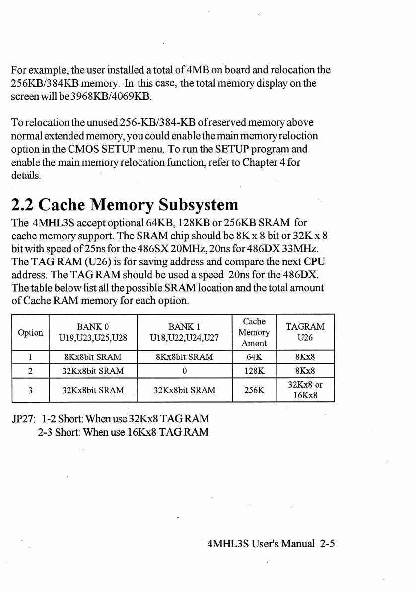
2.2
Cache
Memory
Subsystem
The
41VHL3
S
accept
optional
64KB,128KB
or
256KB
SRAM
for
cache
memory
support.
The
SRAM
chip
should
be
8K
x
8
bit
or
32K
x
8
bit
with
speed
of
25ns
for
the
486SX
20MHz,
20ns
for
486DX
33MHz.
The
TAG
RAM
(U26)
is
for
saving
address
an
d
compare
the
next
CPU
address.
The
TAG
RAM
should
be
used
a
speed
20ns
for
the
486DX.
The
table
below
list
all
the
possible
SRAM
location
an
d
the
total
amount
of
Cache
RAM
memory
for
each
option.
Option
BANK
0
U19,U23,U25,U28
BANK
1
U18,U22,U24,U27
Cache
Memory
Amont
TAGRAM
U26
1
8Kx8bit
SRAM
8Kx8bit
SRAM
64K
8Kx8
2
32Kx8bit
SRAM
0
128K
8Kx8
3
32Kx8bit
SRAM
32Kx8bit
SRAM
256K
32Kx8
or
16Kx8
JP27:
1-2
Short:
When
use
32Kx8
TAG
RAM
2-3
Short:
When
use
16Kx8
TAG
RAM
4MHL3
S
User's.
Manual
2-5

Note
4MHL3
S
User's
Manual
2-6

Chapter
3
Jumper
Jumper
Settings
and
Connectors
This
chapter
will
assist
you
with
setting
-up
the
4MHL3
S
before
you
install
it
in
a
system
case.
If
your
4MHL3
S
has
already
been
installed
and
you
do
not
wish
to
change
the
configuration
settings,
you
can
skip
over
this
section.
3.1
Jumper
Switches
The
4MHL3
S
has
several
jumper
switches
that
must
be
set
to
define
a
system
configuration.
These
Jumper
are
three
-pin
components
on
the
mainboard.
They
are
turned
off
and
on
by
placing
or
removing
a
cover
cap
over
the
pins.
This
is
called
a
open
or
short
jumper.
All
jumpers
must
be
set
to
one
of
the
two
possible
settings.
3.2.1
Cache
RAM
Jumper
Setting
JP
15
JP
16
JP
17
JP
19
JP20
32K
Byte
2-3
Short
Open Open
Open
Open
64K
Byte
1-2
Short
Open
Open
Close
Open
128K
Byte
2-3
Short
2-3
Short
Close
Close
Open
256K
Byte
1-2
Short
1-2
Short
Close Close
Close
Note:
64K
byte
=
8
pieces
of
8K
x
8
SRAM
on
cache
bank
0
and
1
128K
byte
=4
pieces
of
32K
x
8
SRAM
on
cache
bank
0
256K
byte
=
8
pieces
of
32K
x
8
SRAM
on
cache
bank
0
and
1
4MHL3
S
User's
Manual
3-1
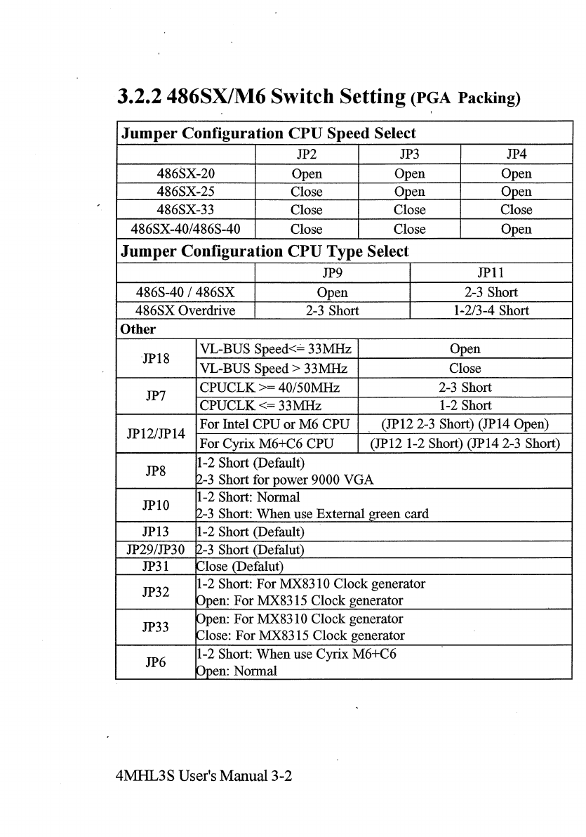
3.2.2
486SX/M6
Switch
Setting
(PGA
Packing)
Jumper
Configuration
CPU
Speed
Select
JP2
JP3
JP4
486SX-20
Open
Open
Open
486SX-25
Close
Open
Open
486SX-33
Close
Close Close
486SX-40/4865-40
Close
Close
Open
Jumper
Configuration
CPU
Type
Select
JP9
JP
11
486S-40
/
486SX
Open
2-3
Short
486SX
Overdrive
2-3
Short
1-2/3-4
Short
Other
JP
18
VL-BUS
Speed<=
33
MHz
Open
VL-BUS
Speed
>
3
3
MHz
Close
JP7
CPUCLK
>=
40/5
0MHz
2-3
Short
CPUCLK
<=
3
3
MHz
1-2
Short
JP
12/JP
14
For
Intel
CPU
or
M6
CPU
(JP
12
2-3
Short)
(JP
14
Open)
For
Cyrix
M6+C6
CPU
(JP
12
1-2
Short)
(JP
14
2-3
Short)
JP8
1-2
Short
(Default)
2-3
Short
for
power
9000
VGA
JP
10
1-2
Short:
Normal
2-3
Short:
When
use
External
green
card
JP
13
1-2
Short
(Default)
JP29/JP3
0
2-3
Short
(Defalut)
JP31
Close
(Defalut)
J1,32
1-2
Short:
For
MX8310
Clockgenerator
Open:
For
MX8315
Clock
generator
W33
Open:
For
MX8310
Clock
generator
Close:
For
MX8315
Clock
generator
JP6
1-2
Short:
When
use
Cyrix
M6+C6
Open:
Normal
4MHL3S
User's
Manual
3-2
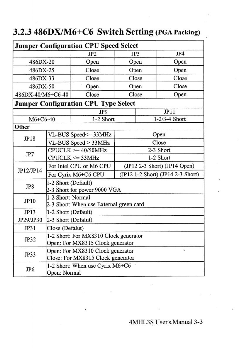
3.2.3
486DX1M6+C6
Switch
Setting
(PGA
Packing)
Jumper
Configuration
CPU
Speed
Select
JP2
JP3
JP4
486DX-20
Open Open Open
486DX-25
Close
Open
Open
486DX-33
Close
Close
Close
486DX-50
Open
Open
Close
486DX-40/M6+C6-40
Close Close
Open
Jumper
Configuration
CPU
Type
Select
JP9
JP
11
M6+C
6-40
1-2
Short
1-2/3-4
Short
Other
JP
18
VL-BUS
Speed<=
33MHz
Open
VL-BUS
Speed
>
33MHz
Close
CPUCLK
>=
40/50M
Iz
2-3
Short
CPUCLK
<=
33MHz
1-2
Short
JP
12/JP
14
For
Intel
CPU
or
M6
CPU
(JP
12
2-3
Short)
(JP
14
Open)
For
Cyrix
M6+C
6
CPU
(JP
12
1-2
Short)
(JP
14
2-3
Short)
JP
8
1-2
Short
(Default)
2-3
Short
for
power
9000
VGA
JP
10
1-2
Short:
Normal
2-3
Short:
When
use
External
green
card
JP
13
1-2
Short
(Default)
JP29/JP30
2-3
Short
(Defalut)
JP31
Close
(Defalut)
JP32
1-2
Short:
For
MX8310
Clock
generator
Open:
For
MX8315
Clock
generator
JP33
Open:
For
MX8310
Clock
generator
Close:
For
MX8315
Clock
generator
J,
6
1-2
Short:
When
use
Cyrix
M6+C6
Open:
Normal
4MHL3
S
User's.
Manual
3-3
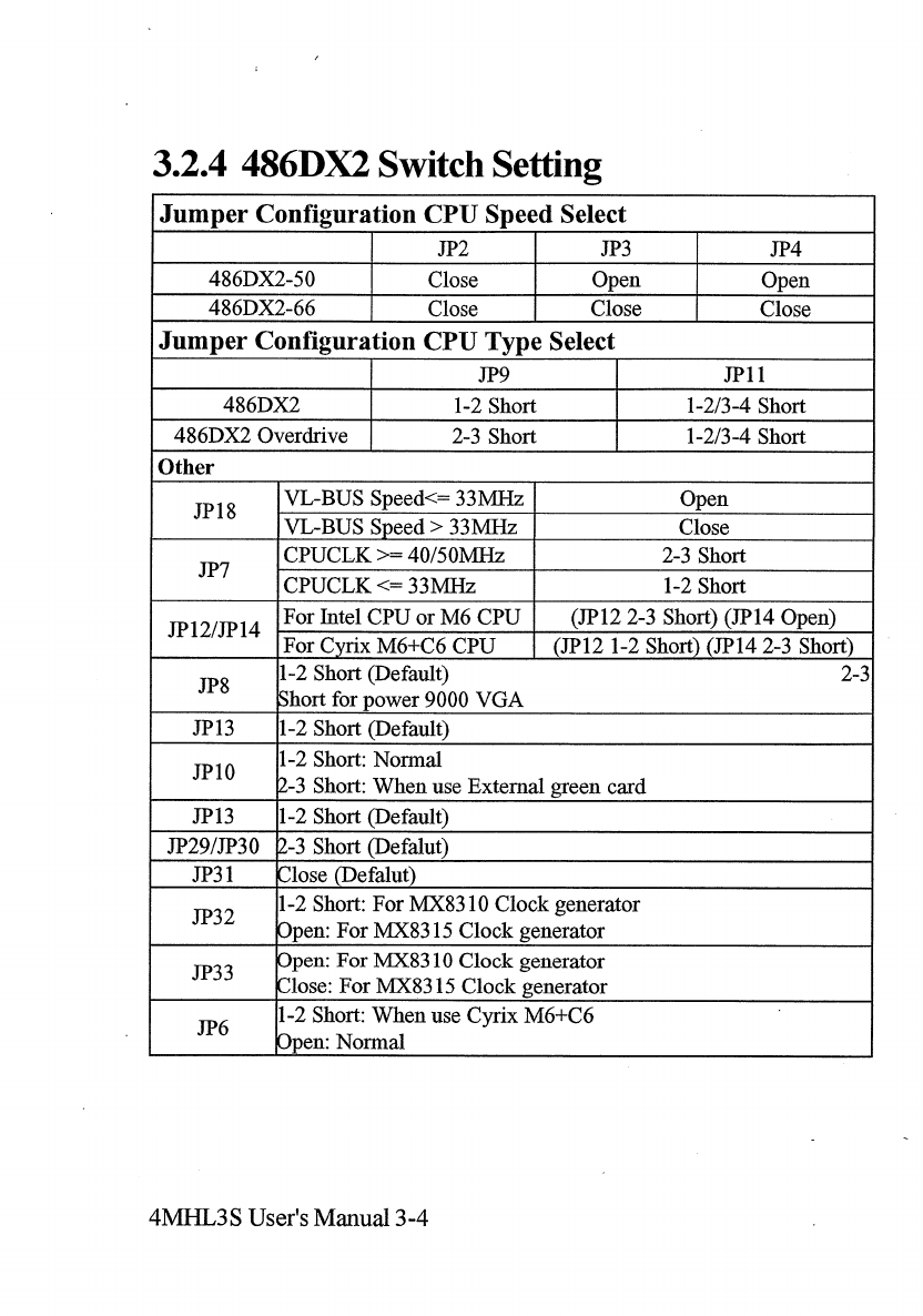
3.2.4
486DX2
Switch
Setting
Jumper
Configuration
CPU
Speed
Select
JP2
JP3
JP4
486DX2-50
Close
Open
Open
486DX2-66
Close
Close Close
Jumper
Configuration
CPU
Type
Select
JP9
JP
11
486DX2
1-2
Short
1-2/3-4
Short
486DX2
Overdrive
2-3
Short
1-2/3-4
Short
Other
JP18
VL-BUS
Speed<=
33MHz
Open
VL-BUS
Speed
>
33MHz
Close
JP7
CPUCLK
>=
40/50MHz
2-3
Short
CPUCLK
<=
33MHz
1-2
Short
JP
12/JP
14
For
Intel
CPU
or
M6
CPU
(JP
12
2-3
Short)
(JP
14
Open)
For
Cyrix
M6+C6
CPU
(JP
12
1-2
Short)
(JP
14
2-3
Short)
JP8
1-2
Short
(Default)
2-3
Short
for
power
9000
VGA
JP
13
1-2
Short
(Default)
JP
10
1-2
Short:
Normal
2-3
Short:
When
use
External
green
card
JP
13
1-2
Short
(Default)
JP29/JP3
0
2-3
Short
(Defalut)
JP31
Close
(Defalut)
JP32
1-2
Short:
For
MX8310
Clock
generator
Open:
For
MX8315
Clock
generator
JP33
Open:
For
MX8310
Clock
generator
Close:
For
MX8315
Clock
generator
J,
6
1-2
Short:
When
use
Cyrix
M6+C6
Open:
Normal
4MHL3S
User's
Manual
3-4

3.3
Connectors
There
are
several
connectors
located
on
the
4M50AIL.
They
are
used
to
connect
with
some
peripheral
devices
to
enhance
the
performance
of
the
system
operation.
Refer
to
Appendix
B
for
the
positions
of
all
the
connectors
on
the
mainboard.
Their
functions
are
listed
below:
Connector
Function
KB
1
Keyboard
Connector
P1
Power
Connector
JP
1
Open:
When
use
EXT
Battery
Close:
When
use
TNT
Battery
JP21
EXT
Battery
Connector
JP22
Keylock
Connector
JP23
Speaker
Connector
JP24
Turbo
LED
Connector
JP25
Turbo
SW
Connector
JP2d
Reset
SW
Connector
JP2$
Green
PC
Connector
4MHL3
S
User's
Manual
3-5

Note
4MIIL3S
User's
Manual
3-6

Chapter
4
Setup
4.1
Built-in
BIOS
Setup
program
This
chapter
provides
detailed
instructions
on
how
to
configure
your
system
using
the
Built-in
BIOS
Setup
Program
and
gives
some
technical
information
about
your
computer.
If
you
are
not
very
familiar
with
microcomputers,
please
carefully
read
this
chapter
before
proceeding.
If
you
do
not
want
to
change
the
system's
configuration,
you.can
skip
this
chapter.
SETUP
program
built
in
the
system
BIOS.
4.1.1
How
to
Recall
the
Setup
Program
You
can
run
the
built-in
SETUP
program
in
several
ways:
1.
When
powering
-on
the
system
When
you
turn
on
the
system
power,
or
press
the
button
on
the
system
case
while
the
system
is
running
(not
every
system
has
this
button),
the
BIOS
will
first
test
the
functionalityof
the
system
components
and
display
a
start-up
message
similar
to
the
following:
XXX
KB
OK
Hit
<Del>
key,
if
you
want
to
run
setup
The
numeral
digits
will
continue
to
count
at
the
top
left
of
the
screen.
This
is
the
BIOS
testing
the
mainboard
memory
chips.
After
the
above
message
disappears,
you
can,
press
the
<Del>
key
to
run
the
Setup
program.
2.
To
reset
the
system
By
pressing
<Ctrl>
<Alt>
<Del>
key
combination
when
the
system
is
up
and
running
(assumingyou
are
running
under
DOS
or
other
environments
that
support
this
feature),
the
system
will
immediately
reset
itself
and
boot
up.
Before
booting
up
from
a
diskette
or
hard
disk,
you
can
also
see
the
below
start-up
message:
4MHL3
S
User's
Manual
4-1
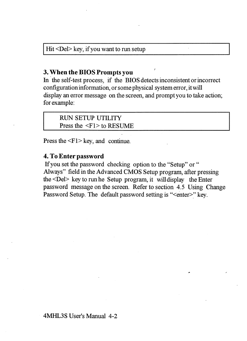
Hit
<Del>
key,
if
you
want
to
run
setup
3.
When
the
BIOS
Prompts
you
In
the
self
-test
process,
if
the
BIOS
detects
inconsistent
or
incorrect
configuration
information,
or
some
physical
system
error,
it
will
display
an
error
message
on
the
screen,
and
prompt
you
to
take
action;
for
example:
RUN
SETUP
UTILITY
Press
the
<F
1
>
to
RESUME
Press
the
<F
1>
key,
and
continue.
4.
To
Enter
password
If
you
set
the
password
checking
option
to
the
"Setup"
or"
Always"
field
in
the
Advanced
CMOS
Setup
program,
after
pressing
the
<Del>
key
to
run
he
Setup
program,
it
will
display
the
Enter
password
message
on
the
screen.
Refer
to
section
4.5
Using
Change
Password
Setup.
The
default
password
setting
is
"<enter>"
key.
4MI-IL3
S
User's
Manual
4-Z
Table of contents
Other EFA Motherboard manuals


