Installation and Configuration
S5U13L01P00C100 Evaluation Board Seiko Epson Corporation 7
Rev. 1.3
Chapter 3 Installation and Configuration
The S5U13L01P00C100 evaluation board incorporates a DIP switch, jumpers, and 0 ohm resistors which allow it
to be used with a variety of different configurations.
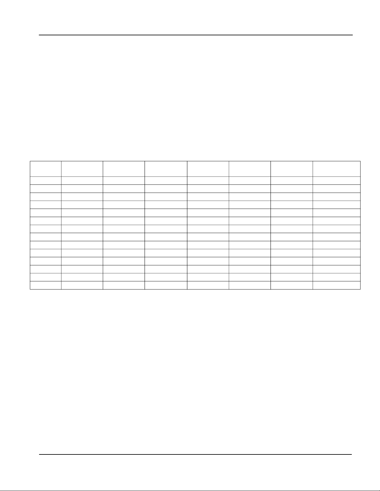
3.1 CNF[2:0] Configuration
The S1D13L01 has 3 configuration inputs CNF[2:0], which are used to configure the S1D13L01 host interface type
through DIP switch SW1. Depending on the CNF[2:0] setting, some host interface pins will not be used. Those pins
should be terminated by SW2 and SW3.
1. For SW2~3, the setting must be Off if there is no suggestion in table.
2. For JP105~109, the setting must be 1-2 if there is no suggestion in table.
3. Low means internal pull-down for address bus active.
4. The SPI interface is not available when the S5U13L01P00C100 evaluation board is used with the
S5U13U00P00C100 USB adapter board.
Table 3-1: Host Interface Pin Mapping
S1D13L01
Pin Name
Direct 16-bit
Mode 1
Direct 16-bit
Mode 2
Indirect 16-bit
Mode 1
Indirect 16-bit
Mode 2 Direct 8-bit Indirect 8-bit SPI
CNF[2:0] 000 001 010 011 100 101 111
CS# CS# CS# CS# CS# CS# CS# CS#
WR# WR# RDU# WR# RDU# WR# WR# SCK
RD# RD# RDL# RD# RDL# RD# RD# SW2-3=On
UB# UB# WRU# UB# WRU# SW2-1=On SW2-1=On SW2-1=On
LB# LB# WRL# LB# WRL# SW2-2=On SW2-2=On SW2-2=On
AB0 TE (JP108 2-3) TE (JP108 2-3) TE (JP108 2-3) TE (JP108 2-3) AB0 TE (JP108 2-3) TE (JP108 2-3)
AB1 AB1 AB1 P/C# P/C# AB1 P/C# Low
AB[18:2] AB[18:2] AB[18:2] Low Low AB[18:2] Low Low
DB0 DB0 DB0 DB0 DB0 DB0 DB0 SI
DB1 DB1 DB1 DB1 DB1 DB1 DB1 SO
DB[7:2] DB[7:2] DB[7:2] DB[7:2] DB[7:2] DB[7:2] DB[7:2] SW2-5~10=On
DB8 DB8 DB8 DB8 DB8 TE (JP108 3-4) SW3-1=On SW3-1=On
DB[15:9] DB[15:9] DB[15:9] DB[15:9] DB[15:9] SW3-2~8=On SW3-2~8=On SW3-2~8=On