EVOC EC7-1813CLD2NA SERIES User manual

EC7-1813CLD2NA SERIES
基于 Intel® Luna Pier 平台 Mini-ITX 主板
Mini-ITX Motherboard Based on Intel®
Luna Pier Platform
Version: C00

CopyrightNotice
Informationofferedinthismanualisbelievedtobecorrectatthetimeofprinting,and
is subject to change without prior notice in order to improve reliability, design and
functionanddoesnotrepresentacommitmentonthepartofthemanufacturer.Inno
event will the manufacturer be liable for direct, indirect, special, incidental, or
consequentialdamagesarisingoutofimproperinstallationand/oruse,orinabilityto
usetheproductordocumentation.
Thisusermanualisprotectedbycopyright.Nopartofthismanualmaybereproduced,
stored in any retrieval system, or transmitted, in any form or by any means,
mechanical,electronic,photocopied,recordedorotherwise,withoutthepriorwritten
permissionfromthemanufacturer.
Trademarks
EVOC is a registered trademark of EVOC Intelligent Technology Co., Ltd. Other
productnamesmentionedhereinareusedforidentificationpurposesonlyandmaybe
trademarkand/orregisteredtrademarksoftheirrespectivecompanies.
Pleasevisitourwebsite:http://www.evoc.com formoreinformation,
Or send to the Technical Support Mailbox support@evoc.com or
support@evoc.cn forconsultation.

SafetyInstructions
1. Pleasereadthismanualcarefullybeforeusingtheproduct;
2. Leavetheboardorcardintheantistaticbaguntilyouarereadytouseit;
3. Touchagroundedmetalobject(e.g.for10seconds)beforeremovingtheboard
orcardfromtheantistaticbag;
4. Beforeinstallingorremovingaboard,weartheESDglovesorESDwriststrap;
handletheboardbyits edgesonly;
5. Beforeinserting,removingorreconfiguringmotherboardsorexpansioncards,
first disconnect the computer and peripherals from their power sources to
preventelectricshocktohumanbodiesordamagetotheproduct;
6. Remember to disconnect the AC power cord fromthesocket before removing
theboardormovingthePC;
7. ForPCproducts,remembertodisconnectthecomputerandperipheralsfromthe
powersourcesbeforeinsertingorremovingaboard;
8. Before connecting or disconnecting any terminal, peripheral or any device, be
surethesystemispoweredoffandallthepowersourcesaredisconnected;
9. Afterturningoffthecomputer,waitatleast30secondsbeforeturningitbackon

Contents
Chapter1ProductIntroduction ................................................................................1
Overview.................................................................................................................1
MechanicalDimensions,WeightandEnvironment....................................................1
TypicalConsumption...............................................................................................2
Microprocessor........................................................................................................2
Chipset....................................................................................................................2
SystemMemory ......................................................................................................2
DisplayFunction .....................................................................................................2
NetworkFunction....................................................................................................3
AudioFunction........................................................................................................3
PowerFeature..........................................................................................................3
ExpansionBus.........................................................................................................3
WatchdogFunction..................................................................................................3
OperatingSystem ....................................................................................................3
OnboardI/O...........................................................................................................4
Chapter2Installation...............................................................................................5
ProductOutline........................................................................................................5
LocationsofConnectors ..........................................................................................6
Structure..................................................................................................................7
JumperSetting.........................................................................................................8
InstalltheSystemMemory.......................................................................................9
SerialPort .............................................................................................................10
DisplayConnector .................................................................................................11
LCDBacklightControlConnector .........................................................................13
AudioConnector ...................................................................................................13

IDEConnector ...................................................................................................... 14
SATAConnector ................................................................................................... 15
HotswapofSATAHardDisk................................................................................ 15
KMConnector ...................................................................................................... 17
LANPortandUSBPort ........................................................................................ 18
ParallelPort .......................................................................................................... 19
GPIOConnector.................................................................................................... 19
PowerConnector................................................................................................... 20
StatusIndicatingandControlConnector ................................................................ 21
FanConnector....................................................................................................... 21
CFCard................................................................................................................ 22
ExpansionSlot...................................................................................................... 23
InstructionsforDVIDisplayOutput ...................................................................... 24
Chapter3BIOSSetup ........................................................................................... 27
BIOSOverview..................................................................................................... 27
BIOSParameterSetup........................................................................................... 27
BasicFunctionSettingforBIOS............................................................................ 28
SystemResourceManagedbyBIOSunderX86Platform....................................... 43
Chapter4InstalltheDrivers.................................................................................. 46
Appendix.............................................................................................................. 47
WatchdogProgrammingGuide.............................................................................. 47
DigitalIOProgrammingGuide.............................................................................. 49
TroubleshootingandSolutions............................................................................... 53

Chapter1ProductIntroduction
EC71813CLD2NASERIES 1
Chapter1ProductIntroduction
Overview
The product is an embedded MiniITX single board based on Intel® Luna Pier
Refresh platform.
The board adopts thetechnique scheme of Intel® Atom™ D510/D410 processor +
Intel®ICH8Monboard.ItprovidesoneSODIMMDDR2slotonboardupto2GB.
It supports three display modes: VGA, 24bit LVDS and DVI; two 10/100/1000M
Ethernet controllers; eight USB2.0 ports; two SATA hard disk connectors; one IDE
connector, one Type I/II CF connector; one HD Audio connector; six or ten serial
ports (one supports RS232/ RS485, two support power supply); one PS/2 KM
connector; one PCI slot; the board adopts the standard ATX power supply or 12V
singlepowersupply.
TheproductadoptsIntel® lowpowerconsumptionsolutionandsupportsmultiCOM,
power supply on serial port, VGA+LVDS dual display, PCI expansionand so on. It
cansatisfytheindustrialrequirementsofPOSandlotterymachines;besides,itcanbe
used in advertising machines, information kiosks, selfservice terminals and other
applicationswhichdonotrequirehighperformanceofthemotherboard.
MechanicalDimensions,WeightandEnvironment
Ø Dimensions: 170mm (L)x177.9mm (W) x41.5mm (H);
Ø NetWeight: 0.436Kg;
Ø OperatingEnvironment:
Temperature: 10°C ~ 60°C;
Humidity: 5% ~ 95% (noncondensing);
Ø StorageEnvironment:
Temperature: 40°C ~ 75°C;
Humidity: 5% ~ 95% (noncondensing);

Chapter 1 Product Introduction
2 EC71813CLD2NASERIES
TypicalConsumption
Thetypicalconsumptionisbasedonthefollowingidlestatusvalues.
1. ThetypicalpowerconsumptionforEC71813CLD2NAD4V10COMisasfollows:
CPU:OnboardIntel®Atom™D4101.66GHz(166*10/L2=512K)
Memory: TranscendDDRII8002GB
HardDisk: HITIACH2TBSATAHDD
Ø +12V@1.55A;+5%/3%;
2. ThetypicalpowerconsumptionforEC71813CLD2NAD5isasfollows:
CPU:Intel®Atom™D510
Memory: DDRII8002GBKingston
HardDisk: Seagate500GBSATA
Ø +3.3V@0.62A;+5%/3%;
Ø +5V@1.15A;+5%/3%;
Ø +12V@0.52A;+5%/3%.
Microprocessor
Intel®Atom™D510 (DualCore)/D410 (SingleCore)processoronboard, integrated
memorycontrollerandgraphicscontroller.
Chipset
Intel® Atom™D510/D410 processor+Intel® ICH8M
SystemMemory
Provides one 200Pin SODIMM DDR2 memory slot, supporting Unbuffered
NonECCmemoryupto 2GB;thememoryfrequencysupportedisupto 667MHz.
DisplayFunction
Ø AdoptsCPU withintegratedgraphicscontroller;

Chapter1ProductIntroduction
EC71813CLD2NASERIES 3
Ø Supports VGA, singlechannel 24bit LVDS and DVI display, among which
24bit LVDS and DVI are homological inputs and the LVDS and DVI are
output in Clone mode; supports VGA + LVDS (or DVI) output in Clone or
expansionmode;supportsthreedisplaymodesandhotswapfunction.
Ø The maximum resolution and refresh frequency supported by VGA is up to
2048×1536@60HzwhilethemaximumresolutionsupportedbyLVDSisupto
1366×768; ThemaximumresolutionsupportedbyDVIisupto1600×1200.
NetworkFunction
Providestwo10/100/1000MbpsLANports:LAN1supportsWakeonLANfunction
whileLAN2supportsLANPXEbooting.
AudioFunction
AdoptsHD standard,supporting MICIN/LINEIN/LINEOUT.
PowerFeature
AdoptsATX/ATpower:ATXpowersupportsACPI1.0bspecificationandthestatus
of S0,S1, S4 andS5; ATpowersupportssingle 12Vpowersupply.
ExpansionBus
Providesone PCI slot,complyingwith PCI2.3 standard.
WatchdogFunction
Ø 255 levels,programmablebyminuteorsecond;
Ø Watchdogtimeoutinterruptorresetsystem.
OperatingSystem
SupportedOSs: WindowsXP,Windows2000 andLinux.

Chapter 1 Product Introduction
4 EC71813CLD2NASERIES
OnboardI/O
Ø One parallel port, supporting SSP/EEP/ECP operating modes and BIOS
modifiesoperatingmode;
Ø Ten serial ports: COM2 supports RS232/RS485 mode selection; COM1
supportsModemwakeupfunction;COM3andCOM4support5V/12Vpower
output;
Ø OneIDEconnector;
Ø OneCF cardconnector;
Ø Two SATA connectors,supportinghotswapfunction;
Ø Eight USB2.0 ports: USB1 ~ USB4 are brought out via connectors directly;
USB5 ~USB8 arebroughtoutin 2x5Pin headers;
Ø Two PS/2keyboard/mouseconnectors:oneisastandardconnectorandtheother
apinheader;
Ø One8channeldigital I/Oconnector.
Tips:howtoidentifythealarms
1.Long“beep”indicates a systemmemoryerror;
2.Shortbeepindicatestopoweronthecomputer.

Chapter2Installation
EC71813CLD2NASERIES 5
Chapter2Installation
ProductOutline
H2 H3
H4
H1
170
170
4.9
154.9
132.1
33
157.5 6.4
Unit: mm
Warning!
Please adopt appropriate screws and proper installation methods (including
boardallocation,CPUandheatsinkinstallation,etc);otherwise,theboardmay
bedamaged.ItisrecommendedtouseM3x6GB9074.488screwsatH1 ~H4.

Chapter 2 Installation
6 EC71813CLD2NASERIES
LocationsofConnectors
H2 H3
H4
H1
AUDIO2
AUDIO1
J4 J3
J2 J1 KM1
JP3
JP4
JP5
JP6
JP2
SYSFAN1
CPUFAN1
COM3
COM4 COM6 COM8 COM10
COM9 COM7 COM5
LCDB1
JLCD1
LVDS1
PWR2
PWR1
PWR3
SATA2
SATA1
JP1 JCF1
DIMM1
CF1
FP2
FP3
FP1
IDE1
J5
J6
JCC1
PCI1
LPT1 GPIO1 KM2
U1
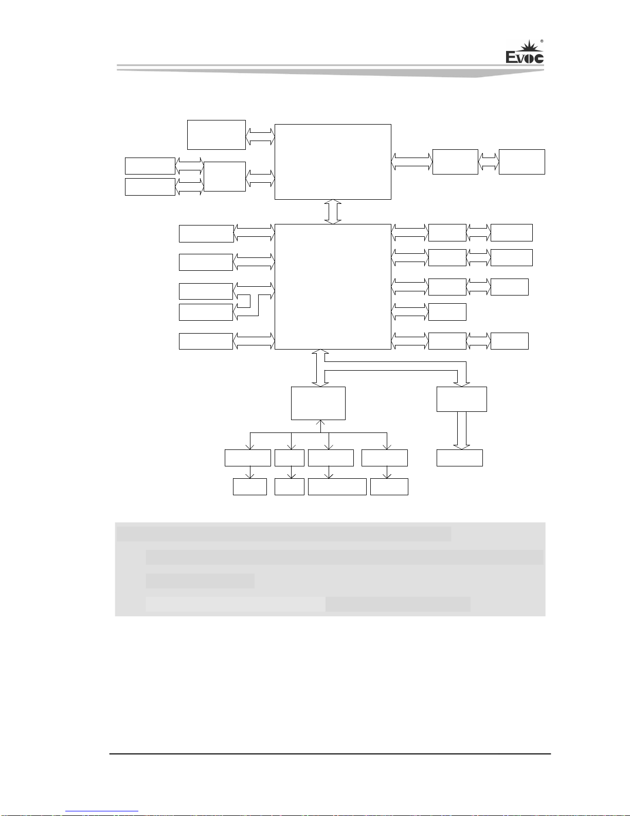
Chapter2Installation
EC71813CLD2NASERIES 7
Structure
LAN2
SATA
CO M 7/ 8/9 /10
(
RS232
插 针)
Ha r dw a re Monit or
HDA
IT8782
RTL8111D
DB15
I DE1(44 pin)
DMI
PCIEPort2
RJ45
W D T
ICH8M
COM 5/6
(RS232)
插 针
P CI
槽
V G A
LAN1
内接插针
标准接口
Para lle l
SMBus
9534
82801HM
DDR2
Terminaltion
COM 1
(RS 232)
Connector
COM 2
(RS 232/485)
COM 3/4(RS232)
插针
第
9PIN
可选
RI/5V/12V
U SB 2.0 X4 (
标 准
)
U SB 2.0 X4 (
插 针
)
LPC B US
SPIFlash
S ATAIIX 2(1*7)
82574L
PCIEPor t1
F81216D
USB
CF1(TYPEII)
D510
(
DC
)
/
D410
(
SC
)
CPU
SPI
PATA
PCI
外接或内接
Connector
PS/2
键鼠
ALC888
插 针
RJ45
8
路
GPIO
CH7036
LVDS 24BIT
DVI
CHA
DD R2S OD IM M1
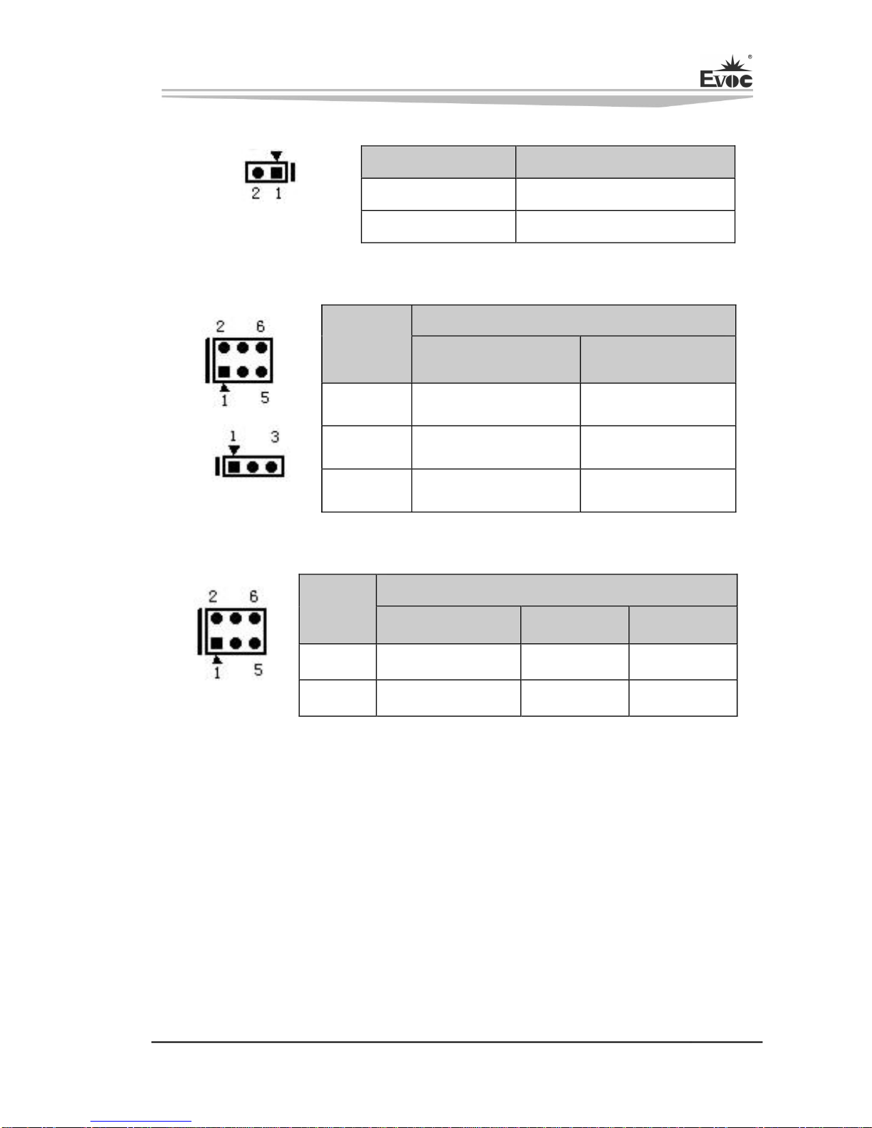
Tip:Howtoidentifythefirstpinofthejumpersandconnectors
1. Observetheletterbesidethesocket,itwouldbemarkedwith“1”orboldlines
ortriangularsymbols;
2. Observethesolderpadontheback; thesquarepadisthefirstpin.

Chapter 2 Installation
8 EC71813CLD2NASERIES
JumperSetting
1. JCC1:Clear/KeepCMOSSetting (Pitch:2.0mm)
CMOS is powered by the button battery on board. Clearing CMOS will restore
original settings (factory default). The steps are listed as follows: (1) Turn off the
computer and unplug the power cable; (2) Instantly short circuitJCC1; (3) Turn on
thecomputer;(4)FollowthepromptonscreentoenterBIOSsetupwhenbootingthe
computer,loadoptimizeddefaults;(5)Saveandexit. Pleasesetasfollows:
JCC1
Setup Function
12Open Normal(Default)
12Short ClearthecontentsofCMOSandallBIOSsettings
willrestoretofactorydefaultvalues.
2. JLCD1: SelectLCDOperating Voltage (Pitch:2.0mm)
Different LCD screens have different voltages; the board provides two voltage
options, +3.3V and +5V. Only when the selected LCD screen voltage is in accord
withtheLCDscreenoperatingvoltageinuse,cantheLCDscreenoperatenormally.
Pleasesetasfollows:
JLCD1
Setup Function
12Short +3.3V(Default)
23Short +5V
3. JCF1: SelectCFCard Operating Voltage (Pitch:2.0mm)
Different CF cards have different voltages; the board provides two voltage options,
+3.3Vand +5V.OnlywhentheselectedCFcardvoltageisinaccordwiththeCFcard
operatingvoltageinuse,canthe system stability beensured.Pleasesetas follows:
JCF1
Setup Function
12Short +3.3V
23Short +5V(Default)
Note:CFcardvoltageselectionaresettocomplywithdifferentCFcards;asfor
the CF cards withoutspecified operating voltages, please choose the operating
voltageaccordingtoactualusage.
Chapter2Installation
EC71813CLD2NASERIES 9
4. JP1:SelectMaterandSlaveModefor CFCard (Pitch:2.0mm)
JP1
Setup Function
12Short Master
12Open Slave(Default)
5. JP2~JP4:SelectModeforSerialPort (Pitch:2.0mm)
JP2
JP3~JP4
Pin
Setting
ModeSelection
RS232 (Default) RS485
JP2 12 34
JP3 12 23
JP4 12 23
6. JP5~JP6: Pin9 FunctionSelectionforCOM3/COM4 (Pitch:2.0mm)
JP5/JP6
Pin
Setting
Pin9 FunctionSelectionfor COM3/COM4
RI#(Default) VCC5V VCC12V
JP5 12 34 56
JP6 12 34 56
InstalltheSystemMemory
The board is configured with one 200Pin DDRII SODIMM slot (DIMM1). When
installing thememorybank,pleasepayattentiontothe following issues:
Ø Open the buckles on both sides of the memory slot. When installing, align the
notch of the memory bank with that of the memory slot and gently insert the
moduleintotheslot;
Ø Thememoryof1.8VDDRII667MHzsupportedbyIntel®Chipsetcanbeused;
the maximummemorycapacitysupportedbytheboardisupto2GB;
Ø ItisrecommendedtousethememorybankwithSPDtoensurestableoperation.

Chapter 2 Installation
10 EC71813CLD2NASERIES
SerialPort
TheboardprovidestwostandardDB9serialports:COM1supportsModemwakeup
function and RS232mode; COM2supports RS232/RS485 modeselection;italso
provides eight 2x5Pin serial ports (Pitch: 2.54mm) of RS232 mode. The pin
definitions areasfollows:
J1(COM1)
Pin SignalName
1 DCD#
2 RXD
3 TXD
4 DTR#
5 GND
6 DSR#
7 RTS#
8 CTS#
9 RI#
J1(COM2)
Pin SignalName
RS232 RS485
1 DCD# Data
2 RXD Data+
3 TXD NC
4 DTR# NC
5 GND GND
6 DSR# NC
7 RTS# NC
8 CTS# NC
9 RI# NC
Note:thedatatransmissiondirectionofCOM2iscontrolledautomaticallyunder
RS485 mode.

Chapter2Installation
EC71813CLD2NASERIES 11
COM3 ~ COM10
Pin SignalName
1 DCD#
2 RXD
3 TXD
4 DTR#
5 GND
6 DSR#
7 RTS#
8 CTS#
9 RI#
10 NA
DisplayConnector
The board provides a set of 24bit single channel LVDS connector and one
VGA+DVID dual layer connector (Marked as J2 onboard: DVI connector for the
upper layer while VGA connector for the lower layer). The pin definitions are as
follows:
1. VGAConnector
J2(VGA)
Pin SignalName Pin SignalName
1 Red 2 Green
3 Blue 4 NC
5 GND 6 GND
7 GND 8 GND
9 NC 10 GND
11 NC 12 DDCDATA
13 HSYNC 14 VSYNC
15 DDCCLK

Chapter 2 Installation
12 EC71813CLD2NASERIES
2. DVIDConnector
J2(DVI)
Pin SignalName Pin SignalName
1 DATA2 13 NC
2 DATA2+ 14 +5V
3 GND_DVI 15 GND
4 NC 16 HOTPLUG
5 NC 17 DATA0
6 DDCCLK 18 DATA0+
7 DDCDATA 19 GND_DVI
8 NC 20 NC
9 DATA1 21 NC
10 DATA1+ 22 GND_DVI
11 GND_DVI 23 CLK+
12 NC 24 CLK
3. Singlechannel24bit LVDS Connector
LVDS1
(Pitch:1.0mm)
Pin SignalName Pin SignalName
1 LVDS_D0+ 2 LVDS_D0
3 GND 4 GND
5 LVDS_D1+ 6 LVDS_D1
7 GND 8 GND
9 LVDS_D2+ 10 LVDS_D2
11 GND 12 GND
13 CLK+ 14 CLK
15 GND 16 GND
17 LVDS_D3+ 18 LVDS_D3
19 VDD 20 VDD
Note: The LVDS socket adopted by the board is DF20G20DP1V while the
correspondingterminaltypeis DF20A20DF1C.

Chapter2Installation
EC71813CLD2NASERIES 13
LCD BacklightControlConnector
Theboardprovidesone1x4PinLCDbacklightcontrolconnector(Pitch:2.0mm);the
pindefinitionsareasfollows:
LCDB1
Pin SignalName
1 VCC_LCDBKLT
2 LCD_BKLTCTL
3 LCD_BKLTEN
4 GND
Note: VCC_LCDBKLT+12Vbacklightpower (Thecurrentislimitedbelow1A);
LCD_BKLTCTLbacklightcontrol(ThesignalisoutputasPWMsignalvia
Pineview D; the voltage amplitude is between 0V3.3Vwhile
thedutycycleisbetween 0% ~ 100%);
LCD_BKLTEN backlightenable,activehigh.
AudioConnector
TheboardprovidesoneduallayerAudio connectorandone2x5PinAUDIOpinheader.
AUDIO1
Pin SignalName
1 LINE_OUT
2 MIC_IN
AUDIO2
(Pitch:2.0mm)
Pin SignalName Pin SignalName
1 LOUT_R 2 LOUT_L
3 GND_AUDIO 4 GND_AUDIO
5 LIN_R 6 LIN_L
7 GND_AUDIO 8 GND_AUDIO
9 MIC_L 10 MIC_R

Chapter 2 Installation
14 EC71813CLD2NASERIES
IDEConnector
TheboardprovidesasetofparallelIDEconnector(Pitch:2.0mm),whichsharesan
IDEbuswiththeCFcardconnector;therefore,pleasepayattentiontothefollowing
issueswheninstallingtheIDEdevices:
Ø If the CF card connector has been occupied with CF storage card, the IDE
connectorcanonlyconnectwithoneIDEdevice;oneisMasterdeviceandthe
otherisSlavedevice,whichcanbesetviaJP1.Therelevantjumperisprovided
ontheharddisktosetittoMasterdeviceorslavedevice;
Ø If the CF card connector is not occupied, the IDE connector canconnect with
twoIDEdevices.ThewayofconnectionistoconnecttheMasterdevicetothe
endofthecablewhileconnecttheSlavedevicetothemiddleofthecable;when
usinganUltra66/100harddisk,80pinappropriativeflatcableshallbeadopted.
IDE1
Pin SignalName Pin SignalName
1 RESET# 2 GND
3 D7 4 D8
5 D6 6 D9
7 D5 8 D10
9 D4 10 D11
11 D3 12 D12
13 D2 14 D13
15 D1 16 D14
17 D0 18 D15
19 GND 20 Key
21 DREQ 22 GND
23 IOW# 24 GND
25 IOR# 26 GND
27 IORDY 28 GND
29 DACK# 30 GND

Chapter2Installation
EC71813CLD2NASERIES 15
31 IRQ 32 NC
33 DA1 34 ATA66_DET
35 DA0 36 DA2
37 CS1# 38 CS3#
39 LED# 40 GND
41 +5V 42 +5V
43 GND 44 GND
SATA Connector
Theboardprovidestwo SATA sockets;thepindefinitionsareasfollows:
SATA1/SATA2
Pin SignalName
1 GND
2 TX+
3 TX
4 GND
5 RX
6 RX+
7 GND
HotswapofSATAHardDisk
NoticesforhotswapofSATA hard disk:
1. The hard disk shall support SATA 2.0 and use 15pin SATA hard diskpower
connector.
2. ThedriverofchipsetshallsupportthehotswapofSATAharddisk.
3. HotswapofSATAharddiskwiththeoperatingsystemisforbiddenwhensystem
ispoweredon.
SATA DataCable SATA PowerCable
Table of contents
Other EVOC Motherboard manuals

EVOC
EVOC EC3-1813 Series User manual

EVOC
EVOC 104-1814CLDNA Series User manual

EVOC
EVOC EC0-1818-C236 User manual

EVOC
EVOC NET-1821VD2N User manual

EVOC
EVOC EC3-1820V2NA User manual

EVOC
EVOC EC5-1817LNAR User manual

EVOC
EVOC EC7-1817LNAR User manual

EVOC
EVOC EC7-1818CLD2NA User manual

EVOC
EVOC CPC-3813CLD3N User manual

EVOC
EVOC 104-1649CLD2NA Series User manual


