EVOC CPC-1814CLD5NA-N User manual

CPC-1814CLD5NA-N
双核宽温 6U Compact PCI 主板
Dual Core & Wide Temperature 6U
Compact PCI Motherboard
Version: C02

Copyright Notice
Information offered in this manual is believed to be correct at the time of printing, and
is subject to change without prior notice in order to improve reliability, design and
function and does not represent a commitment on the part of the manufacturer. In no
event will the manufacturer be liable for direct, indirect, special, incidental, or
consequential damages arising out of improper installation and/or use, or inability to
use the product or documentation.
This user manual is protected by copyright. No part of this manual may be reproduced,
stored in any retrieval system, or transmitted, in any form or by any means,
mechanical, electronic, photocopied, recorded or otherwise, without the prior written
permission from the manufacturer.
Trademarks
EVOC is a registered trademark of EVOC Intelligent Technology Co., Ltd. Other
product names mentioned herein are used for identification purposes only and may be
trademark and/or registered trademarks of their respective companies.
Please visit our website: http://www.evoc.com for more information,
Or send to the Technical Support Mailbox support@evoc.com or

Safety Instructions
1. Please read this manual carefully before using the product;
2. Leave the board or card in the antistatic bag until you are ready to use it;
3. Touch a grounded metal object (e.g. for 10 seconds) before removing the board
or card from the anti-static bag;
4. Before installing or removing a board, wear the ESD gloves or ESD wrist strap;
handle the board by its edges only;
5. Before inserting, removing or re-configuring motherboards or expansion cards,
first disconnect the computer and peripherals from their power sources to
prevent electric shock to human bodies or damage to the product;
6. Remember to disconnect the AC power cord from the socket before removing
the board or moving the PC;
7. For PC products, remember to disconnect the computer and peripherals from the
power sources before inserting or removing a board;
8. Before connecting or disconnecting any terminal, peripheral or any device, be
sure the system is powered off and all the power sources are disconnected;
9. After turning off the computer, wait at least 30 seconds before turning it back on.

Contents
Chapter 1 Product Introduction ..................................... 1
Overview ......................................................................................................................1
Environment and Mechanical Dimensions ...................................................................1
Typical Power Consumption.........................................................................................2
Microprocessor .............................................................................................................2
Chipset..........................................................................................................................2
Memory ........................................................................................................................2
Display Function...........................................................................................................2
LAN Function...............................................................................................................2
Audio Function.............................................................................................................3
On-board IO..................................................................................................................3
Watchdog Function.......................................................................................................3
Power Feature...............................................................................................................3
Chapter 2 Installation ............................................. 4
Product Outline.............................................................................................................4
Locations of Connectors ...............................................................................................5
Structure .......................................................................................................................6
Jumper Setting ..............................................................................................................7
CPCI Hot-swappableMicro-switch..............................................................................8
JTAG Connector ...........................................................................................................9
USB ..............................................................................................................................9
LPC Connector ...........................................................................................................10
Display Connector ......................................................................................................10
SATA Connector .........................................................................................................11

LAN Port ....................................................................................................................11
Serial Port ...................................................................................................................12
GPIO Connector .........................................................................................................13
Indicator......................................................................................................................13
Reset Button ...............................................................................................................13
Compact Flash Connector...........................................................................................14
Compact PCI Connector.............................................................................................15
PMC Connector ..........................................................................................................19
Chapter 3 BIOS Setup .............................................. 22
BIOS Overview ..........................................................................................................22
BIOS Parameter Setup................................................................................................22
Basic Function Setting for BIOS ................................................................................23
System Resource Managed by BIOS under X86 Platform .........................................33
Appendix .......................................................... 37
GPIO Program Guide .................................................................................................37
Watchdog Programming Guide...................................................................................43
Troubleshooting and Solutions ...................................................................................45

Chapter 1 Product Introduction
CPC-1814CLD5NA-N - 1 -
Chapter 1 Product Introduction
Overview
CPC-1814CLD5NA-N contains Intel® GME965 + Intel® ICH8M chipset, Intel®
CoreTM 2 Duo L7500 high-performance and low-power processor and dual-channel
DDRII memory on-board, up to 2GB. As for graphics processing, it deploys Intel®
GME965 chipset integrated with GMA X3100 graphics chip and supports
VGA+LVDS (DVI) independent dual-display (optional between LVDS and DVI). It
also complies with the specifications such as PICMG2.0, PICMG2.1, PICMG2.10,
PICMG2.11 and PICMG2.16 etc.
CPC-1814CLD5NA-N provides one 10/100/1000Mbps LAN port, one digital IO
connector, one 2.5″SATA hard disk connector, a set of 32bit PCI PMC connector or
one CompactFlash connector, one serial port, two USB ports and one VGA connector.
CPC-1814CLD5NA-N is a wide-temperature 6U Compact PCI motherboard, which
can meet requirements for different connectors together with the rear IO board,
CPC-RP804B and CPC-RP804R. It mainly targets high-end CPCI applications, such
as information communication, network storage, network audio process, network
graphics processing, industrial control and military sector, etc.
Environment and Mechanical Dimensions
Dimensions: 233.4mm (L) x 161.50mm (W) x 20.3mm (H);
Net Weight: 820.9g;
Operating Environment: Temperature: L7500: -40 ~ 80C; T7500: -10 ~ 60C
Humidity: 5% ~ 95% (non-condensing);
Temperature: -40C ~ 80C (Forced air cooling when the environment
temperature is above 60℃)
System Fan Speed: ≥1.41m/s
Storage Environment: Temperature: -40C ~ 85C;
Humidity: 5% ~ 95% (non-condensing);

Chapter 1 Product Introduction
- 2 - CPC-1814CLD5NA-N
Typical Power Consumption
L7500: 30.89W
CPU: Intel/L7500/1.60GHz/L2 4MB/FSB800MHz on-board
Memory: Samsung/DDRII667/2GB on-board
[email protected]; +5%/-3%;
[email protected]; +5%/-3%;
[email protected]; +5%/-3%;
T7500: 45.48W
CPU: Intel/T7500/2.20GHz/L2 4MB/FSB800MHz on-board
Memory: Samsung/DDRII667/2GB on-board
[email protected]; +5%/-3%;
[email protected]; +5%/-3%;
[email protected]; +5%/-3%;
Microprocessor
Intel® CoreTM 2 Duo L7500 high-performance and low-power processor, complying
with Intel® CoreTM 2 Duo T7500 high-performance and low-consumption processor;
which provides excellent performance and can meet the growing requirement for
system data processing.
Chipset
Intel® GME965 + ICH8M
Memory
DDRII memory on-board up to 2GB with excellent compatibility, providing stable
memory data exchange environment.
Display Function
Intel® GME965 chipset integrated with GMA X3100 graphics chip, supporting VGA
display and LVDS and DVI alternative display with maximum resolution up to
1920x1080.
Note: the rear IO boards, CPC-RP804B and CPC-RP804R, support DVI display with
1024x768 maximum resolution.

Chapter 1 Product Introduction
CPC-1814CLD5NA-N - 3 -
LAN Function
Three 10/100/1000Mbps LAN ports, two of which are brought out via rear
IO board, CPC-RP804B or CPC-RP804R.
Two 10/100/1000Mbps LAN ports, realizing PICMG 2.16 package exchanging
function via CPCI connector.
Audio Function
One HD Audio connector brought out via rear IO board.
On-board IO
Two serial ports (CPC-1814CLD5NA-N has one on board while the IO board
brings out the other one; the serial port on rear IO board supports
RS-232/RS-422/RS-485 mode);
Three SATA connectors (CPC-1814CLD5NA-N has one on board while the IO
board brings out the other two);
Two SAS connectors, brought via rear IO board;
Four USB ports (two are brought out via rear IO board);
One keyboard and mouse connector (brought out from rear IO board);
One digital IO connector;
A set of PMC connector or a Compact Flash connector (optional according to
the board type).
Watchdog Function
1-255 seconds or 1-255 minutes, 255 levels;
Watchdog timeout interrupt or reset system.
Power Feature
Supplies power via carrier.

Chapter 2 Installation
- 4 - CPC-1814CLD5NA-N
Chapter 2 Installation
Product Outline
PTH7
PTH6
PTH10
PTH9
PH1
PTH5
PH3
PH4
PH2
233.4
161.5
168.7
PTH8
Unit (mm)
Warning!
Please adopt appropriate screws and proper installation methods (including
board allocation, CPU and heat sink installation, etc); otherwise, the board may
be damaged. It is recommended to use GB 818 M2.5x5 screws at PH1 ~ PH4 and
PTH5 ~ PTH10.

Chapter 2 Installation
CPC-1814CLD5NA-N - 5 -
Locations of Connectors
J5
JN2
JN4
JN1
CF1
JCF1
LPC1
GPIO1
VGA1
USB1USB2
COM1LAN1
D13D14
RST1
JP3
JTAG1
JP7 SATA1
SW1
J1 J2 J3
PTH7
PTH6
PTH10
PTH9
PTH8
PH1
PTH5
PH3
PH4
PH2
SW2
PMC1

Chapter 2 Installation
- 6 - CPC-1814CLD5NA-N
Structure
SPI Flash
SATA*2
PCI EXPRESS X16
ICH8M-E
GLCI
DDR2
Terminaltion
SPI
82566
NINEVEH
EKRON
GMCH
DDR2
Terminaltion
DIMM2
CH B
DDR2
DMI PCI-E x4
LCI
ME
AGTL+ Bus
CompactPCI Connectors J3/J5
Control Link
GM965E
INTEL MEROM
CPU(T7500/L7500)
LVDS
PCI Express x1 *2
82573E*2
USB2.0 *2
PCI-Express X1 *2
83627DHG LPC BUSCOM1
COM2
USB
USB2.0 *2
SATA*1
SATA
Audio DVI-ICOM2LAN2,3 SAS 1,2,
SATA 2,3 LVDS
VGA
LANConnector
Transformer
PCIE x4 to PCI-X DIMM1
CH A
DDR2
HDA Audio
VGAVGA
Tip: How to identify the first pin of the jumpers and connectors
1. Observe the letter beside the socket, it would be marked with “1” or bold lines
or triangular symbols;
2. Observe the solder pad on the back; the square pad is the first pin.

Chapter 2 Installation
CPC-1814CLD5NA-N - 7 -
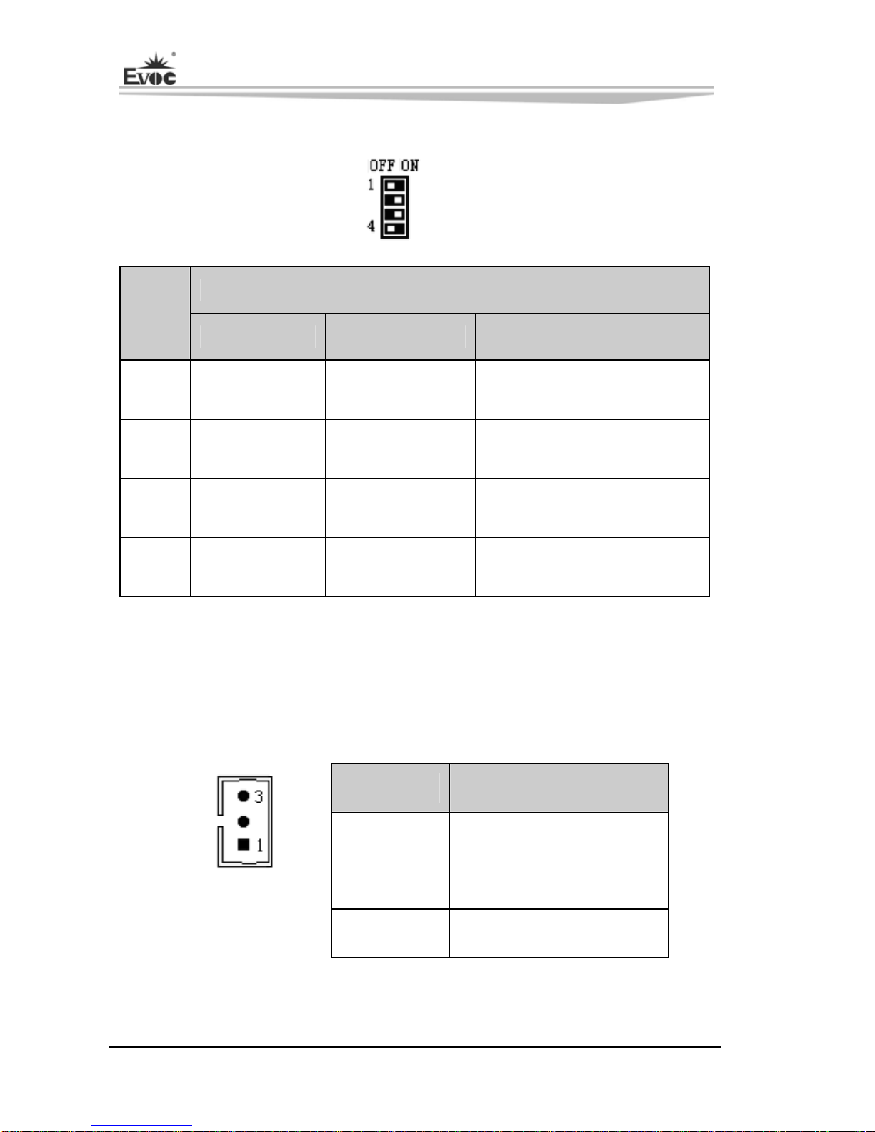
Jumper Setting
JCF1: Select CF Card Operating Voltage (Pitch: 2.0mm)
Select the CF card operating voltage by changing the status of JCF1.
Setup Voltage
[1-2] Short +3.3V(Default)
JCF1 [2-3] Short +5V
Note: the motherboard sets the CF card voltage selection jumper to ensure that
the CF card of certain type can operate at one voltage option at least. It is
recommended to use the 3.3V jumper setting for the CF card.
SW1: PI7C9x130 Bridge Dip Switch
SW1 is the dip switch to configure PI7C9x130, which has been set before delivery.
Please set as follows:
System Status
SW1
Switch ON=0 OFF=1
1 Non-NT(Default) NT
2
3
SW1
4
Used to adjust the operating frequency of the bridge chip.
When adopting default setting, the operating frequency is
33MHz. When 4=OFF, the peripheral card can select
b
etween 66MHz and 33MHz automatically; if the
peripheral card doesn’t support automatic selection, then
the operating frequency is 66MHz. (Default: 2=ON;
3=OFF; 4=OFF)
Note: When CPC-8408B-A089 complete PC is used,
the default setting for SW1 Pin4 on the motherboard is
4=ON. (Default: 2=ON, 3= OFF, 4=ON).
Chapter 2 Installation
- 8 - CPC-1814CLD5NA-N
SW2: Select Operating Mode for PI7C9x130 Bridge
SW2
System Status
SW2
Switch ON=0 OFF=1 Function
1 GND(Default) REVRSB
Forward (=0) and Backward (=1)
Mode Selection
2 GND TM1(Default)
EEPROM (=0) and SMBus (=1)
Selection
3 GND MSK_IN(Default) Enable (=1)/Disable (=0) Bridge
Hot-swap Function
4 GND(Default) CFN_L
Internal (=0) and External (=1)
Arbitrary Selection
Note: forward mode indicates that the PI7C9x13 Bridge is converted from PCIE
to PCI bus while backward mode indicates that the PI7C9x13 Bridge is
converted from PCI to PCIE bus.
CPCI Hot-swappable Micro-switch
Pin Signal Name
1 VCC3
2 GND
JP3
(Pitch: 1.25mm) 3 EJECT

Chapter 2 Installation
CPC-1814CLD5NA-N - 9 -
JTAG Connector
Record the data required by CPLD via JTAG1 on-board.
Pin Signal Name
1 VCC
2 GND
3 TCK
4 TDO
5 TDI
JTAG1 (Pitch: 2.54mm)
6 TMS
Setup Function
[1-2] Short Reset PCIe signal (Default)
JP7 (Pitch: 2.0mm) [2-3] Short Reset PCI signal
USB
The board provides two standard USB ports.
Pin Signal Name
1 +5V
2 USB_Data-
3 USB_Data+
USB1/USB2 4 GND
Chapter 2 Installation
- 10 - CPC-1814CLD5NA-N
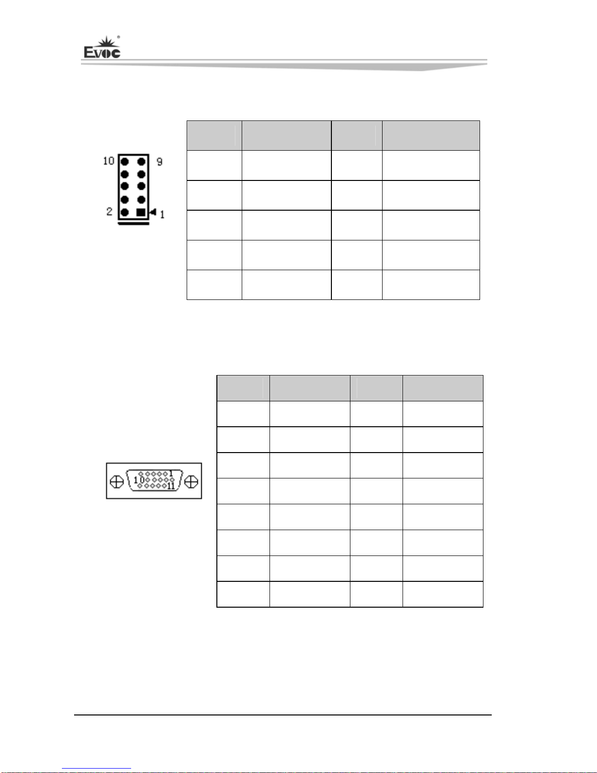
LPC Connector
LPC1 is a connector for debugging.
Pin Signal Name Pin Signal Name
1 VCC 2 LPC_AD3
3 L_FRAME# 4 LPC_AD2
5 RESET# 6 LPC_AD1
7 DIS# 8 LPC_AD0
LPC1
(Pitch: 2.0mm)
9 GND 10 PCI_CLK
Display Connector
The board provides one 15-pin D-sub VGA display connector.
Pin Signal Name Pin Signal Name
1 Red 2 Green
3 Blue 4 NC
5 GND 6 GND
7 GND 8 GND
9 NC 10 GND
11 NC 12 DDCDATA
13 HSYNC 14 VSYNC
VGA1
15 DDCCLK
Note: when using with the rear IO boards, CPC-RP804B&CPC-RP804R, please pay
attention that the VGA connector of the rear IO board and that of the motherboard are
alternative, so as to avoid asynchronous display or other problems.

Chapter 2 Installation
CPC-1814CLD5NA-N - 11 -
SATA Connector
The board provides a 7+15Pin SATA connector.
SATA1
Pin Signal Name Pin Signal Name
A1 GND B5 GND
A2 TX+ B6 GND
A3 TX- B7 +5VL
A4 GND B8 +5V
A5 RX- B9 +5V
A6 RX+ B10 GND
A7 GND B11 GND
B1 +3.3V B12 GND
B2 +3.3V B13 +12VL
B3 +3.3VL B14 +12V
B4 GND B15 +12V
LAN Port
The board provides one 10/100/1000Mbps LAN port. ACTLED and LILED are the
LEDs beside the Ethernet port, which respectively indicates the activity status and
transmission status of LAN. Please refer to the status description for each LED:
MX0, MX0-: positive/negative data
channel 0
MX1, MX1-: positive/negative data
channel 1
MX2, MX2-: positive/negative data
channel 2
MX3, MX3-: positive/negative data
channel 3
ACTLED: LAN activity status indicator LILED: LAN linked status indicator
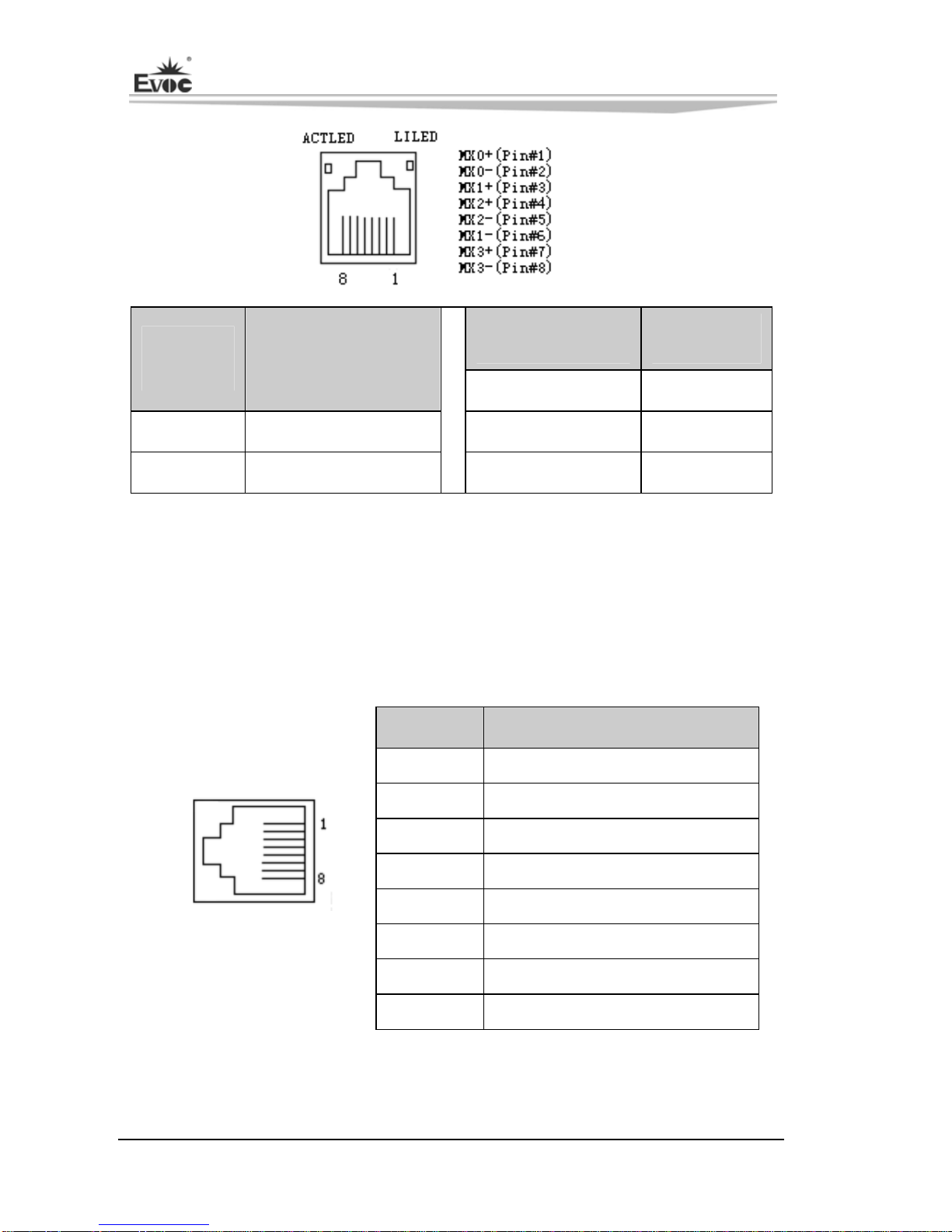
Chapter 2 Installation
- 12 - CPC-1814CLD5NA-N
LAN1
LILED
(Dual-Color: O/G) LAN Speed
Indicator
ACTLED
(Green)
LAN Activity
Status Indicator Green 1000Mbps
Blink Data Transmitting Orange 100Mbps
Off No Data to Transmit Off 10Mbps
Note: the LAN port doesn’t support wake-up function.
Serial Port
The board provides a serial communication connector (RJ45), which can connect with
devices with standard RS-232 connectors, such as mouse, modem and digital camera,
etc.
Pin Signal Name
1 RTS#
2 DTR#
3 TXD
4 GND
5 GND
6 RXD
7 DSR#
COM1
8 CTS#
Note: the serial port doesn’t support wake-up function.

Chapter 2 Installation
CPC-1814CLD5NA-N - 13 -
GPIO Connector
The board provides a set of GPIO connector, 4 for input while the other 4 for output.
Pin Signal Name Pin Signal Name
1 GPIO1 2 GPIO5
3 GPIO2 4 GPIO6
5 GPIO3 6 GPIO7
7 GPIO4 8 GPIO8
GPIO1 (Pitch: 2.0mm)
9 GND 10 NC
Note: the factory default value is that Pin 1, 3, 5, and 7 are for input while Pin 2,
4, 6 and 8 are for output.
Indicator
LED Status Description
OFF Hard disk is idle
HDD ON Hard disk is operating
OFF Power failure
PW ON Power normal
OFF Normal operating status
HS ON At hot-swapping status
OFF Cannot operate watchdog
WDT ON Operate the watchdog
Reset Button
Pin Signal Name Pin Signal Name
1 RESET# 2 GND
RST1 3 GND_Chassis 4 GND_Chassis

Chapter 2 Installation
- 14 - CPC-1814CLD5NA-N
Compact Flash Connector
The CF card is at Master status in system. The pin definitions of the Compact Flash
slot are as follows (Marked as CF1 in figure).
Pin Signal Name Pin Signal Name
1 GND 26 CD1#
2 D3 27 D11
3 D4 28 D12
4 D5 29 D13
5 D6 30 D14
6 D7 31 D15
7 CS0# 32 CS1#
8 GND 33 VS1#
9 ATASEL# 34 IOR#
10 GND 35 IOW#
11 GND 36 WE#
12 GND 37 IRQ
13 VCC 38 VCC
14 GND 39 CSEL#
15 GND 40 VS2#
16 GND 41 RESET#
17 GND 42 IORDY
18 A2 43 DREQ
19 A1 44 DACK#
20 A0 45 DASP#
21 D0 46 ATA66_DET
22 D1 47 D8
23 D2 48 D9
24 WP/IOCS16# 49 D10
25 CD2# 50 GND
Chapter 2 Installation
CPC-1814CLD5NA-N - 15 -
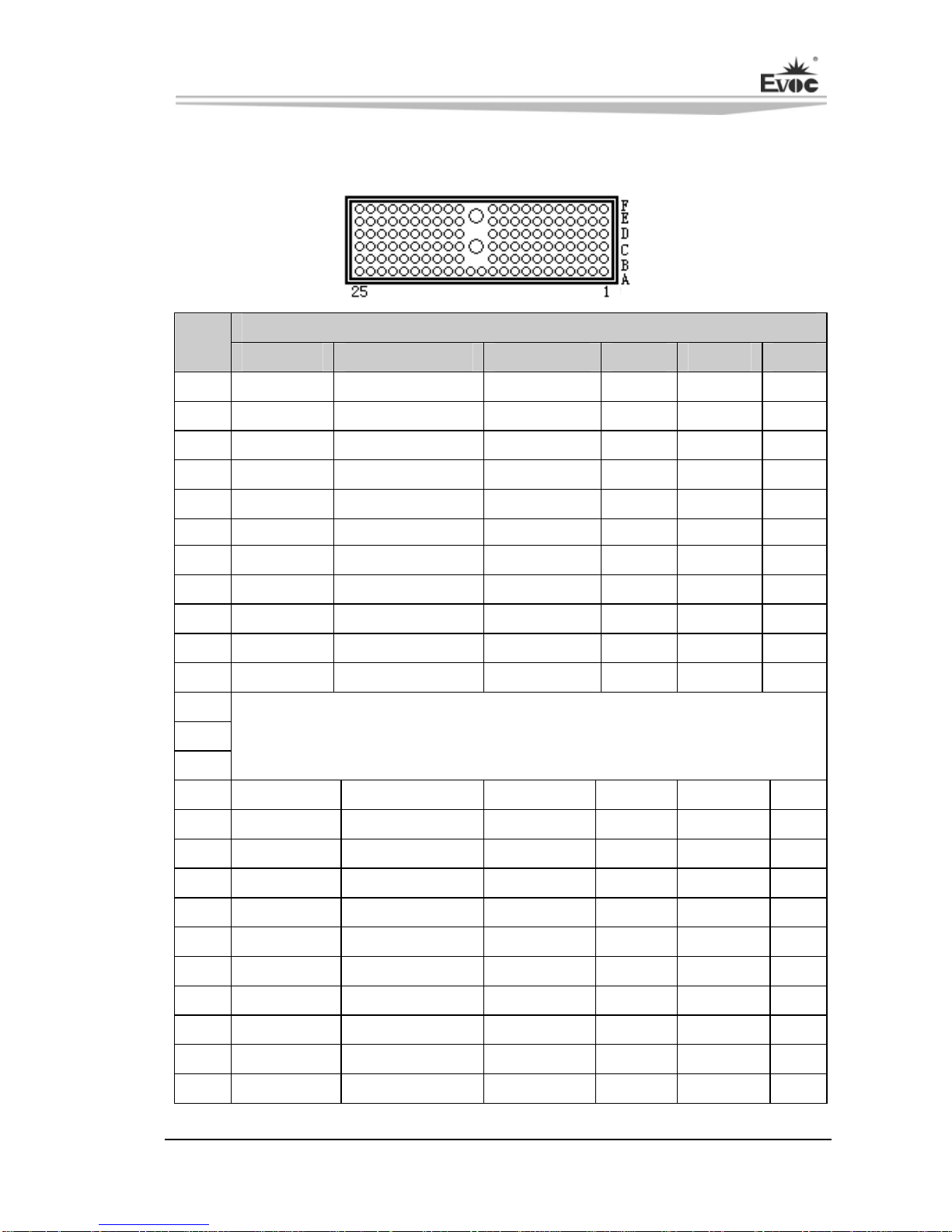
Compact PCI Connector
The pin definitions of J1
J1
Signal Name
Pin A B C D E F
1 +5V -12V TRST# +12V +5V GND
2 TCK +5V TMS# TDO TDI GND
3 INTA# IRQB# INTC# +5V INTD# GND
4 IPMB_PWR HEALTHY# V(I/O) INTP INTS GND
5 NC NC PCI_RST# GND GNT0# GND
6 REQ0# PCI_PRESENT# +3.3V CLK0 AD31 GND
7 AD30 AD29 AD28 GND AD27 GND
8 AD26 GND V(I/O) AD25 AD24 GND
9 C/BE3# GND AD23 GND AD22 GND
10 AD21 GND +3.3V AD20 AD19 GND
11 AD18 AD17 AD16 GND C/BE2# GND
12
13
14
KEY AREA
15 +3.3V FRAME# IRDY# BD_SEL# TRDY# GND
16 DEVSEL# GND V(I/O) STOP# LOCK# GND
17 +3.3V IPMB_SCL IPMB_SDA GND PERR# GND
18 SERR# GND +3.3V PAR C/BE1# GND
19 +3.3V AD15 AD14 GND AD13 GND
20 AD12 GND V(I/O) AD11 AD10 GND
21 +3.3V AD9 AD8 M66EN C/BE0# GND
22 AD7 GND +3.3V AD6 AD5 GND
23 +3.3V AD4 AD3 +5V AD2 GND
24 AD1 +5V V(I/O) AD0 ACK64# GND
25 +5V REQ64# ENUM# +3.3V +5V GND
Table of contents
Other EVOC Motherboard manuals

EVOC
EVOC 104-1814CLDNA Series User manual

EVOC
EVOC CPC-3813CLD3N User manual

EVOC
EVOC EC0-1814 User manual

EVOC
EVOC EC7-1817LNAR User manual

EVOC
EVOC EC0-1815V2NAR User manual

EVOC
EVOC NET-1821VD2N User manual

EVOC
EVOC ec3-1813cld2na User manual

EVOC
EVOC EC5-1817LNAR User manual

EVOC
EVOC EC7-1818CLD2NA User manual

EVOC
EVOC EC7-1813CLD2NA SERIES User manual


