Icom IC-R75 User manual

SERVICE
MANUAL
COMMUNICATIONS RECEIVER

This service manual describes the latest service information
for the IC-R75 at the time of publication. NEVER connect the receiver to an AC outlet or to a DC
power supply that uses more than 16 V. Such a connection
could cause a fire hazard and/or electric.
DO NOT expose the receiver to rain, snow or any liquids.
DO NOT reverse the polarities of the power supply when
connecting the receiver.
DO NOT apply an RF signal of more than 20 dBm (100mW)
to the antenna connector. This could damage the receiver's
front end.
Be sure to include the following four points when ordering
replacement parts:
1. 10-digit order numbers
2. Component part number and name
3. Equipment model name and unit name
4. Quantity required
<SAMPLE ORDER>
0910051123 PCB B-5274C IC-R75 PLL UNIT 1 pieces
8810005770 Screw Bih M3x8 ZK IC-R75 Chassis 10 pieces
Addresses are provided on the inside back cover for your
convenience.
1. Make sure a problem is internal before disassembling
the receiver.
2. DO NOT open the receiver until the receiver is discon-
nected from its power source.
3. DO NOT force any of the variable components. Turn
them slowly and smoothly.
4. DO NOT short any circuits or electronic parts. An insulat-
ed turning tool MUST be used for all adjustments.
5. DO NOT keep power ON for a long time when the receiv-
er is defective.
6. READ the instructions of test equipment thoroughly
before connecting equipment to the receiver.
To upgrade quality, all electrical or mechanical parts and
internal circuits are subject to change without notice or
obligation.
VERSION
U.S.A.
Europe
U.K.
S.E.Asia
Other
SYMBOL
USA
EUR
UK
SEA
OTH
INTRODUCTION DANGER
ORDERING PARTS REPAIR NOTES

TABLE OF CONTENTS
SECTION 1 SPECIFICATIONS
SECTION 2 INSIDE VIEWS
SECTION 3 CIRCUIT DESCRIPTION
3-1 RECEIVER CIRCUITS . . . . . . . . . . . . . . . . . . . . . . . . . . . . . . . . . . . . . . . . . . . . . . . . . . . . .3-1
3-2 PLL CIRCUITS . . . . . . . . . . . . . . . . . . . . . . . . . . . . . . . . . . . . . . . . . . . . . . . . . . . . . . . . . . .3-4
3-3 LOGIC CIRCUITS . . . . . . . . . . . . . . . . . . . . . . . . . . . . . . . . . . . . . . . . . . . . . . . . . . . . . . . .3-5
3-4 POWER SUPPLY CIRCUITS . . . . . . . . . . . . . . . . . . . . . . . . . . . . . . . . . . . . . . . . . . . . . . . .3-6
3-5 PORT ALLOCATIONS . . . . . . . . . . . . . . . . . . . . . . . . . . . . . . . . . . . . . . . . . . . . . . . . . . . . .3-7
SECTION 4 ADJUSTMENT PROCEDURES
4-1 PREPARATION . . . . . . . . . . . . . . . . . . . . . . . . . . . . . . . . . . . . . . . . . . . . . . . . . . . . . . . . . .4-1
4-2 PLL ADJUSTMENT . . . . . . . . . . . . . . . . . . . . . . . . . . . . . . . . . . . . . . . . . . . . . . . . . . . . . . .4-2
4-3 RECEIVER ADJUSTMENT . . . . . . . . . . . . . . . . . . . . . . . . . . . . . . . . . . . . . . . . . . . . . . . . . .4-4
4-4 SET MODE ADJUSTMENT . . . . . . . . . . . . . . . . . . . . . . . . . . . . . . . . . . . . . . . . . . . . . . . . .4-7
SECTION 5 PARTS LIST
SECTION 6 MECHANICAL PARTS AND DISASSEMBLY
SECTION 7 SEMI-CONDUCTOR INFORMATION
SECTION 8 BOARD LAYOUTS
8-1 PHONE AND VR BOARDS . . . . . . . . . . . . . . . . . . . . . . . . . . . . . . . . . . . . . . . . . . . . . . . . .8-1
8-2 DISPLAY BOARD . . . . . . . . . . . . . . . . . . . . . . . . . . . . . . . . . . . . . . . . . . . . . . . . . . . . . . . . .8-3
8-3 LOGIC BOARD . . . . . . . . . . . . . . . . . . . . . . . . . . . . . . . . . . . . . . . . . . . . . . . . . . . . . . . . . .8-5
8-4 PLL UNIT . . . . . . . . . . . . . . . . . . . . . . . . . . . . . . . . . . . . . . . . . . . . . . . . . . . . . . . . . . . . . . .8-6
8-5 MAIN UNIT . . . . . . . . . . . . . . . . . . . . . . . . . . . . . . . . . . . . . . . . . . . . . . . . . . . . . . . . . . . . .8-7
SECTION 9 BLOCK DIAGRAM
SECTION 10 VOLTAGE DIAGRAM
10-1 FRONT UNIT . . . . . . . . . . . . . . . . . . . . . . . . . . . . . . . . . . . . . . . . . . . . . . . . . . . . . . . . . . . .10-1
10-2 PLL UNIT . . . . . . . . . . . . . . . . . . . . . . . . . . . . . . . . . . . . . . . . . . . . . . . . . . . . . . . . . . . . . . .10-2
10-3 MAIN UNIT . . . . . . . . . . . . . . . . . . . . . . . . . . . . . . . . . . . . . . . . . . . . . . . . . . . . . . . . . . . . .10-3

1 - 1
MGENERAL
• Frequency range :
*1Specifications guaranteed for 0.1 – 29.99 MHz and 50 – 54 MHz
*2Specifications guaranteed for 0.1 – 29.99 MHz
• Mode : SSB (LSB, USB), AM, FM, CW, RTTY, S-AM
• Receive system : Triple-conversion superheterodyne
• Intermediate frequencies :
May differ according to selected IF filter.
• Sensitivity : 0.1 MHz – 1.799 MHz (Preamplifiers are OFF)
SSB, CW, RTTY less than 2.0 µV for 10 dB S/N
AM, S-AM less than 13.0 µV for 10 dB S/N
1.8 MHz – 27.99 MHz (The preamplifier 1 is ON)
SSB, CW, RTTY less than 0.16 µV for 10 dB S/N (typical)
AM, S-AM less than 2.0 µV for 10 dB S/N
28 MHz – 29.99 MHz (The preamplifier 1 is ON)
SSB, CW, RTTY less than 0.16 µV for 10 dB S/N (typical)
AM, S-AM less than 2.0 µV for 10 dB S/N
FM less than 0.5 µV for 12 dB SINAD
50 MHz – 54 MHz (The preamplifier 2 is ON)
SSB, CW, RTTY less than 0.13 µV for 10 dB S/N (typical)
AM, S-AM less than 1.0 µV for 10 dB S/N
FM less than 0.25 µV for 12 dB SINAD
• selectivity : SSB, CW, RTTY More than 2.1 kHz/–6 dB
Less than 4.0 kHz/–60 dB
AM, S-AM More than 6.0 kHz/–6 dB
less than 20.0 kHz/–50 dB
FM More than 12.0 kHz/–6 dB
less than 30.0 kHz/–40 dB
• Audio output power : More than 2.0 W at 10 % distortion with an 8 Ωload
• Antenna impedance : 50 Ωor 450 Ω
• Squelch sensitivity (threshold):
*Preamplifiers are OFF; *1Preamplifier 1 is ON; *2Preamplifier 2 is ON
• Current drain (13.8 V DC) : Less than 1.3 A (Standby), Less than 1.5 A (Max. audio out)
• Spurious and image rejection : More than 70 dB (0.1 – 1.799 MHz SSB, AM, S-AM are more than 60 dB)
• Dimensions : 241(W)×94(H)×229(D) mm; 91⁄2(W)×311⁄16(H)×91⁄32(D) inch (projection not included)
• Weight (approximate) : 3.0 kg; 6 lb 10 oz (AC adaptor “AD–55/A/V” is not included)
• Antenna connector : SO-239 (50 Ω), push connection terminal (450 Ω)
• CI-V connector : 2-connector 3.5 (d) mm (1⁄8")/8 Ω
• PHONES connector : 3-conductor 6.35 (d) mm (1⁄8")
• External speaker connector : 2-conductor 3.5 (d) mm (1⁄8")/8 Ω
SECTION 1 SPECIFICATIONS
All stated specifications are subject to change without notice or obligation.
1st (MHz)
2nd (MHz)
3rd (MHz)
SSB
69.0115
9.0115
0.4550
CW
69.0106
9.0106
0.4559
RTTY
69.0105
9.0105
0.4560
AM, S-AM
69.0100
9.0100
0.4500
FM
69.0115
9.0115
0.4500
Frequency (MHz)
0.1 – 1.799
1.8 – 27.99
28 – 29.99
50 – 54
SSB
less than 71 µV*
less than 5.6 µV*1
–
less than 5.6 µV*2
FM
–
–
less than 0.32 µV*1
less than 0.32 µV*2
Frequency coverage
30 kHz – 60 MHz*1
30 kHz – 30 MHz*2
Version
USA, EUR,
UK, OTH
SEA

2 - 1
SECTION 2 INSIDE VIEWS
2nd IF filter
(FI761: FL-272)
3rd LO circuit
3rd mixer circuit
(IC811)
BFO circuit
2nd IF circuit
PLL IC (IC21)
Noise blaker circuit
VCO circuit
BFO mixer circuit
(IC1101)
Bandpass filter
Fuse (3A)
MAIN UNIT PLL UNIT
Back up battery
(BT 1521)
3rd IF filter
(FI851)
2nd mixer circuit
1st IF filter (FI701)
1st mixer circuit

SECTION 3 CIRCUIT DESCRIPTION
3 - 1
3-1 RECEIVER CIRCUITS
3-1-1 RF SWITCHING CIRCUIT (MAIN UNIT)
The IC-R75 has two antenna connectors. RF signals enter
either the [50 ΩANT.] or [450 ΩANT.] connector.
RF signals from the [50 ΩANT.] connector are applied to the
antenna switching circuit (RL121), and then pass through the
low-pass filter (L131, L132, C131–C136).
RF signals from the [450 ΩANT.] connector are passed
through the L101 to exchange the impeadance value, and
are then applied to the antenna switching circuit (RL121).
The signals are applied to the low-pass filter (L131, L132,
C131–C136).
Each RF signals from the [50 ΩANT.] connector or [450 Ω
ANT.] connector are chosen by the antenna switching circuit
(RL121).
3-1-2 RF FILTER CIRCUIT (MAIN UNIT)
The filtered signals are applied to the RX attenuator switch-
ing circuit (RL141). Either the signals bypass or pass through
the attenuator circuit. The signals are attenuated at 20 dB
when passing through the attenuators. The attenuator sys-
tem excludes non-linear components between an antenna
connector and an attenuator to prevent strong signals from
causing distortion. The signals are then applied to the RF fil-
ters. The MAIN UNIT has 8 RF bandpass fileters for signals
above 2.0 MHz and 2 low-pass filters for signals below 2.0
MHz.
(1) Below 1.6 MHz
The signals are applied to the low-pass filter consisting of
C170–C175, L171–L173 via the limitter circuit (D141, D142).
Adiode is removed at the entrance of the low-pass filter. This
device prevents the diode from causing distortion when
receiving very strong signals. A switching diode (D172) is
turned on when the “B0” line is “HIGH”.
(2) Above 1.6 MHz
The signals are applied to the high-pass filter consisting of
C161–C163, L161–L164. This filter suppresses strong sig-
nals below 1.6 MHz such as broadcasting stations.
The filtered signal between 1.6 MHz and 2.0 MHz are applied
to the low-pass filter (C182–C187, L182, L183) via the
switching diode (D181). The switching diodes (D181, D182)
are turned ON when the “B1” line is “HIGH”.
The filtered signals above 2.0 MHz are applied to one of 8
bandpass filters depending on the receive frequencies.
After passing through a bandpass or low-pass filter, the sig-
nals are applied to the pre-amplifier circuit (Q381, Q382,
IC391).
(3) FILTER SWITCHING CIRCUIT
The RF bandpass filter corresponds to the BPF switching
voltage (B0–B9) based on the CPU via the shifit registor
(IC551, IC552) and driver (IC561, IC562). The switching volt-
age of the BPF exit ot improve multi-signal and strong signal
characteristics.
• RF bandpass and preamplifier circuit
ANT1 (50 Ω)
ANT2 (450 Ω)
ATT (20 dB)
HPF
LPF
0.5 – 1.6 MHz
1.6 – 54 MHz
ATT (10 dB)
LPF
B0
1.6 – 2.0 MHz
B1
BPF
2.0 – 4.0 MHz
B2
BPF
50 – 60 MHz
B9
PRE
AMP
Q381, Q382
PRE
AMP
IC391
LPF
60 MHz to 1st mixer
(Q441, Q442)
preamplifier circuit

3 - 2
3-1-3 PRE-AMPLIFIER CIRCUIT (MAIN UNIT)
The pre-amplifier circuit uses low noise junction FETs (Q381,
Q382) or wideband amplifier (IC391) to provide gain over a
wide frequency range.
When the [P.AMP] switch is turned “PREAMP 1”, the signals
from the RF filter are amplified by the junction FETs pre-
amplifier circuit (Q381, Q382).
When the [P.AMP] switch is turned “PREAMP 2”, the signals
from the RF filter are amplified by the wideband pre-amplifi-
er circuit (IC391).
When the [P.AMP] switch is turned “PREAMP OFF”, the sig-
nals from the RF filter bypass the pre-amplifiers through
D371 and D372.
The amplified or bypassed signals are applied to the 1st
mixer circuit (Q441, Q442) via the low-pass filter (L431, L432
and C431–CC436). The low-pass filter attenuates at 50 MHz
to suppress image frequency.
3-1-4 1ST MIXER AND IF CIRCUITS (MAIN UNIT)
The filtered signals are mixed with a 69.0415–129.0115 MHz
1st LO signal to produce a 69.01 MHz 1st IF signal at the 1st
mixer circuit (Q441, Q442).
The 1st mixer circuit employs a balanced mixer using low-
noise junction FETs (Q441, Q442) to expand the dynamic
range.
The 69.0415–129.0115 MHz 1st LO signal is applied to an
LO amplifier (Q411) from the PLL unit via J411, and then
passes through the low-pass filter (L421, L422, C422–C425).
The filtered signal is applied to the 1st mixer circuit.
The 1st IF signal is applied to the crystal bandpass filter(FI-
461) to suppress out-of-band signals. The filtered signal is
amplified at a 1st IF amplifier (Q471), and then applied to a
2nd mixer circuit (D491)
3-1-5 2ND MIXER AND IF CIRCUITS (MAIN UNIT)
The 1st IF signal is mixed with a 60.0 MHz 2nd LO signal to
produce 9 MHz 2nd IF signal at the 2nd mixer (D491, C492,
L491, L492). The 60.0 MHz 2nd LO signal is applied to the
2nd mixer from the PLL unit via J491.
The 9 MHz 2nd IF signal is applied to the crystal bandpass
filter (FI701) to suppress unwanted signals.
The filtered signal enters the noise blanker gate
(D711–D714). The signal is applied to L712 to obtain clear
reception and is then amplified at the 2nd IF amplifier (Q721).
The signal passes through a loose resonator circuit (C726,
L721) and then is applied to one of the two crystal bandpass
filters.
MODE
LSB, USB, FM
CW
RTTY
AM, S-AM
FREQUENCY
69.0115 MHz
69.0106 MHz
69.0105 MHz
69.0100 MHz
1ST IF FREQUENCY
• IF circuit
Received
signals
1st LO signal
59.0155–129.0115 MHz
BPF IF
AMP
Q441, Q442
1st mixer
Q471
2nd LO signal
60 MHz
D491
2nd mixer
NB
GATE
Noise
Blanker
IF
AMP
Q721 3 kHz
BPF
BPF
Option
Buffer
Q801
Option
BPF
BPF
3 kHz
BPF
6 kHz
BPF
15 kHz
IF
AMP
Q891
IF
AMP
Q911,
Q912
IC811
3rd mixer
3rd LO signal
9.4665 MHz
IC1101
BFO circuit
BFO signal
455 kHz
IF
AMP
Q1001
FM
detector
de-
emphasis
Buffer
AM
detector
AGC
detector
AGC
AMP
IC1001,
X1001
IC1211D
IC2001,
Q2021,
X2021
Q1031
D1061
Q1063
"AGC" signal
AF
selector
IC1201
LPF
PWR
AMP
AF signal
MODE
LSB, USB, FM
CW
RTTY
AM, S-AM
FREQUENCY
9.0115 MHz
9.0106 MHz
9.0105 MHz
9.0100 MHz
2ND IF FREQUENCY

3 - 3
When the [FIL] switch is turned “2F3K”, the filter is selected
FI761 which covering the 2.4 kHz bandwith.
When the [FIL] switch is turned “2FOP”, the filter is selected
an optional filter.
When the [FIL] switch is turned “2FTH”, the signal from the
2nd IF amplifier bypass the crystal bandpass filters through
D771 and D773.
The filtered or bypassed signal is amplified at the buffer
amplifier (Q801) and applied to the 3rd mixer circuit (IC811).
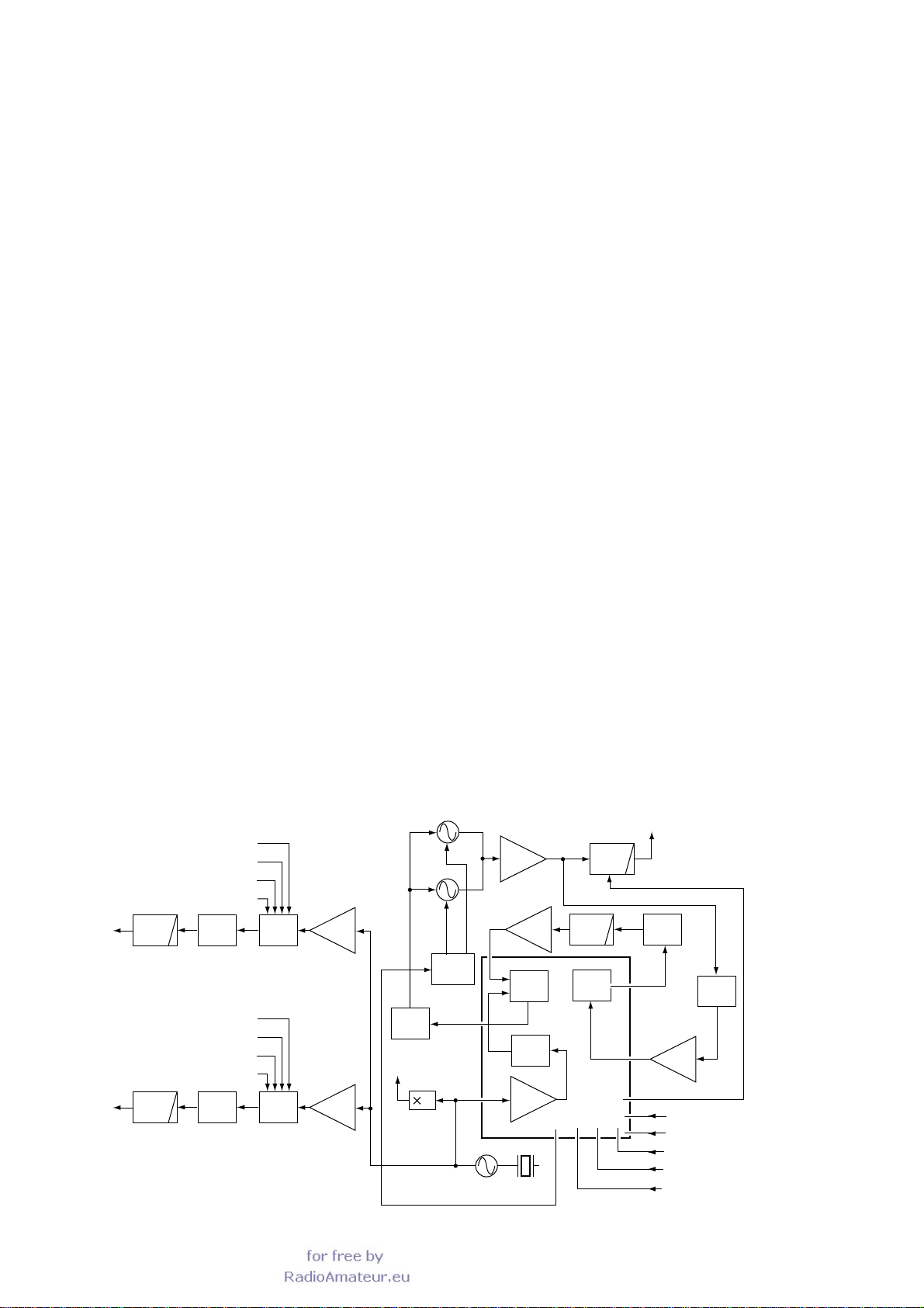
3-1-6 NOISE BLANKER CIRCUITS (MAIN UNIT)
The IC-R75 uses a trigger noise blanker circuit which
removes pulse-type noise signals at the noise blanker gate
(D711–D714).
The 2nd IF signal passes through the crystal bandpass filter
(FI701) to suppress unwanted signals.A portion of the output
signal is applied to a noise amplifier circuit (IC731, Q731,
Q733) and detected at a noise detector circuit (D731). The
detected voltage is applied to a noise blanker gate control cir-
cuit (Q735–Q737, D732).
The threshold level of the noise blanker gate control circuit
(Q735–Q737, D732) is set at 1.0 V on SSB mode (In case of
AM mode, is set at 1.6 V). When the detected voltage
exceeds the threshold level, Q737 outputs a blanking signal
to activate the noise blanker gate (D711–D714).
A portion of the detected voltage is applied to the noise
blanker AGC circuit (Q732, Q734). The noise components
are fed back to the noise amplifier (IC731). The time constant
of the noise blanker AGC circuit is determined by R737,
R744 and C739. This AGC circuit does not operate to detect
pulse-type noise.
When the operating frequency or mode is changed, the
“UNLC” signal is applied to the noise blanker gate control cir-
cuit (D732). The noise blanker gate prevents PLLclick noise.
3-1-7 3RD MIXER AND IF CIRCUITS (MAIN UNIT)
The 2nd IF signal is mixed with a 9.4665 MHz 3rd LO signal
to produce a 450–456 kHz 3rd IF signal at the 3rd mixer
(IC811).
The 9.4665 MHz 3rd LO signal is applied to the 3rd mixer IC
(IC811, pin 10) from the PLL unit via J811. The 450–456 kHz
3rd IF signal is applied either to one of the 3 ceramic band-
pass filters (FI851, FI861, FI871) or to an optional crystal
bandpass filter to suppress unwanted signals.
When the [FIL] switch is turned “3F3K”, the filter is selected
FI851 which covering the 2.4 kHz bandwith.
When the [FIL] switch is turned “3F6K”, the filter is selected
FI861 which covering the 6 kHz bandwith.
When the [FIL] switch is turned “3F15”, the filter is selected
FI871 which covering the 15 kHz bandwith.
When the [FIL] switch is turned “3FOP”, the filter is selected
an optional crystal bandpass filter.
When the mode is selected SSB mode, the filtered 3rd IF sig-
nal is amplified at the 3rd IF amplifier (Q891), and is then
applied to the 3rd IF amplifier (Q911) via the receiver total
gain control circuit (R898). The amplified signal is applied to
the SSB demodulator circuit.
When the mode is selected FM mode, the filtered 3rd IF sig-
nal is amplified at the 3rd IF amplifier (Q891), and is then
applied to the FM demodulator circuit.
When the mode is selected AM mode, the filtered 3rd IF sig-
nal is amplified at the 3rd IF amplifier (Q891), and is then
applied to the 3rd IF amplifier (Q911) via the receiver total
gain control circuit (R898). The amplified signal is applied to
the AM demodulator circuit.
1st, 2nd and 3rd IF amplifiers (Q471, Q721, Q891) are con-
trolled by AGC bias voltage.
3-1-8 BFO CIRCUIT (PLL UNIT)
The BFO (Beat Frequency Oscillator) circuit consists of Q1,
X1, Q201 and IC 201 on PLL unit. The oscillator provides a
beat frequency signal to the SSB demodulator circuit (MAIN
UNIT; IC1101) for demodulating the 3rd IF signal into an AF
signal.
The 30 MHz signal is oscillated at Q1 and X1 for the system
clock signal of the DDS IC (IC201). The oscillated signal is
amplified at Q201 and is applied to the DDC IC (IC201, pin
7) to produce the 455 kHz BFO signal.
The 455 kHz signal passes through the low-pass filter (L201,
L202, C202–C207) via the D/A converter, and is then mixed
with the 3rd IF signal at the SSB demodulator circuit (MAIN
unit; IC1101).
3-1-9 DEMODULATOR CIRCUIT (MAIN UNIT)
The demodulator circuit consists of 3 detector circuits.
(1) SSB DEMODULATOR CIRCUIT
A product detector (IC1101) demodulates SSB, RTTY and
CW signals into an AF signal. The 3rd IF signal from the IF
amplifier (Q911) is mixed with the BFO signal at the product
detector (IC1101) to be demodulated into an AF signal. The
AF signal passes through the AF input mode selector switch
(IC1201).
(2) FM DEMODULATOR CIRCUIT
A FM detector (IC1001, X1001) demodulates the FM signal
into an AF signal. The 3rd IF signal from the IF amplifier
(Q891) is amplified at the 3rd IF amplifier (Q1001), and is
then applied to the FM detector (IC1001, X1001) to demodu-
late the 3rd IF signal. The demodulated signal is applied to
the de-emphasis circuit (IC1211D) to produce the FMAF sig-
nal. The AF signal passes through the AF input mode selec-
tor switch (IC1201).
MODE
LSB, USB
CW
RTTY
AM, S-AM
FREQUENCY
455.0 kHz
455.9 kHz
456.0 kHz
450.0 kHz
3RD IF FREQUENCY

3 - 4
The FM detector outputs “FMNL” signal from IC1001, pin 14
is applied to the CPU (LOGIC unit; IC101, pin 94) to control
the noise squelch level.
(3) AM DEMODULATOR CIRCUIT
The AM demodulater circuit (IC2001) has the envelope
detect function and the synchronous detect function.
An AM detector (IC2001) demodulates the AM signal into an
AF signal. The 3rd IF signal from the IF amplifier (Q911) is
amplified at the buffer amplifier (Q1031), and is then applied
to the AM demodulater circuit (IC2001)to demodulate the 3rd
IF signal into the AM AF signal. The AF signal which is the
AM envelope detect the AF signal or the AM synchronous
detect AF signal passes through the AF input mode selector
switch (IC1201).
3-1-10 AF INPUT MODE SELECTOR SWITCH
(MAIN AND LOGIC UNITS)
The AF input mode selector switch (MAIN unit; IC1201) con-
sists of 4 analog switches. The switches are selected mode
signals of “AFS1” and “AFS2” from the CPU (LOGIC unit;
IC101) via the shift registor (MAIN unit; IC1601), and are
selected by the squelch control signal from the CPU (LOGIC
unit; IC101). TheAF signal is output from IC1201 (MAIN unit;
pin 13).
3-1-11 AF AMPLIFIER CIRCUIT
(MAIN AND FRONT UNITS)
The AF signal output is passed though the low-pass filter
(IC1211) to suppress unwanted signals. The filtered signal is
mixed with “BEEP” signal at the AF level variable circuit
(MAIN unit; IC1251), and is then applied to the AF amplifier
circuit and the AF level variable circuit (IC1251).
The AF level variable circuit controls the AF level by the “AF
GAIN” (R141) on the VR BOARD. TheAF signal is applied to
the AF mute circuit to suppress the noise when “AF GAIN”
(R141) level is minimum, and is then power-amplified at
IC1291 on the MAIN unit to drive the speaker.
The one of the AF amplified signal is output “AAFO” signal to
record the AF signal to the AF recording jack (PLL unit; J3).
3-1-12 AGC AND S-METER CIRCUITS (MAIN UNIT)
TheAGC (Automatic Gain Control) circuit reduces signal fad-
ing and keep the audio output level constant. The receiver
gain is determined by voltage on the AGC line (Q1063, col-
lector). When strong signals are received, the AGC circuit
decreases the voltage on this line.
The 3rd IF signal is amplified at the IF amplifier (Q911).Apor-
tion of the 3rd IF signal is applied to the buffer amplifier
(Q1031) to convert the impedance. The amplified IF signal is
detected at the AGC detector (D1061) via the C1061, and
enters the base of the AGC amplifier (Q1063) to control the
voltage on the AGC line.
The AGC mode is selected by the receiver mode or AGC
swtich on the front panel using the delay control circuit
(Q1064–Q1066). The MDAT signal from the CPU (LOGIC
board; IC101, pin 21) is applied to the shift resistor (IC1601,
pin 2) to produce the AGSS and the AGFS signals. The
AGSS signal is applied to the Q1064, the AGFS signal is
applied to the Q1065, the AGRS signal from the CPU
(LOGIC unit; IC101, pin 80) is applied to the Q1066 to con-
trol the delay control circuit.
The AGRS signal resets the AGC circuit when IC-R75 is
working the memory scaning.
When the AGC switch is selected “OFF”, the Q1061 do not
supply the voltage to the AGC amplifier (Q1063) via the
“AGOS” line, determining the time constant to deactivate the
AGC circuit.
A portion of the AGC bias voltage is amplified at the S-Meter
amplifier circuit (IC1211C, D831), and then applied to the
CPU (LOGIC unit; IC101, pin 95) via the “SML” line. Thus,
the CPU controls S-Meter display.
3-1-13 SQUELCH CIRCUIT
(MAIN AND LOGIC UNIT)
The “SML” signal is applied to the CPU (LOGIC unit; IC101,
pin 91) from the meter amplifier circuit (IC1211C, D831). The
CPU compares “SML” signal with the level of SQL volume on
the VR BOARD to control the “SQL” signal.
The CPU is output the “SQLS” signal from pin 81, and then
applied to the AF selector circuit (MAIN unit; IC1201, pin 6)
which has also the squelch gate circuit.
3-2 PLL CIRCUITS
3-2-1 GENERAL DESCRIPTION
The PLL unit generates a 1st LO signal (69.0415–129.0115
MHz variable), 2nd LO signal (60 MHz), 3rd LO signal
(9.4665 MHz) and BFO signal (455 kHz) used in the MAIN
unit.
The IC-R75 uses a DDS (Direct Digital synthesizer) system.
The DDS system provides rapid lockup time and high quality
frequency oscillation.
3-2-2 REFERENCE OSCILLATOR CIRCUIT
(PLL CIRCUIT)
The 30 MHz reference oscillator circuit consists of X1 and
Q1. The 30 MHz reference frequency is oscillated to produce
all of the LO signals.
3-2-3 1ST LO CIRCUIT (PLL AND MAIN UNIT)
The 30 MHz reference frequency is applied to the DDS-IC
(PLL unit; IC21, pin 40) to oscillate the 1st LO signal. The
reference frequency is compared to the DDS output signal
(PLL unit; IC21, pin 46) to oscillate the PLL lock voltage. The
PLL lock voltage controlls the oscillate frequency of the
VCO1 and VCO2 circuit.

3 - 5
The oscillated signal at the VCO1 and VCO2 circuit is ampli-
fied at the LO-amplifier (PLL unit; Q91), and passes through
the low-pass filter (PLL unit; Q92, D91, D92, L91, L93,
C96–C100, C102, C103) to supperss high harmonic compo-
nents. The low-pass filter controlls the cut-off frequency of
less than 29.999 MHz and more than 30.000 MHz by switch-
ing C102 and C103 “ON” and “OFF” respectively.
The filtered signal is applied to the LO-amplifier (MAIN unit;
Q411), and is then applied to the 1st mixer circuit (MAIN unit;
Q441, Q442) via the low-pass filter (MAIN unit; L421, L422,
C422–C425).
The reference frequency from the LO-amplifier (PLL unit;
Q91) is also divided by 4 at IC22, and is amplified at the
IC23. The signal is applied to the DDS-IC (PLLunit; IC21, pin
88) for the clock signal.
3-2-4 2ND LO CIRCUIT (PLL AND MAIN UNIT)
The 30 MHz reference frequency from the Q1 and X1 on the
PLL unit is multiplied by 2 at Q2 on the PLL unit. The 60 MHz
2nd LO signal is obtained at the L4 and L5 on the MAIN unit,
and is then applied to the 2nd mixer circuit (MAIN unit; D491)
via the 3dB attenuator (MAIN UNIT; R491–R493).
3-2-5 3RD LO CIRCUIT (PLL AND MAIN UNIT)
The 30 MHz reference frequency is oscillated at the Q1 and
X1 on the PLL unit, and is then amplified at the Q151 on the
PLL unit. The amplified signal is applied to the 10 bits DDS-
IC (PLL unit; IC151, pin 7) for the clock signal to produce the
9.4665 MHz 3rd LO signal. The 3rd LO signal is applied to
the D/A converter circuit, and passes through the low-pass
filter (PLL unit; L151, L152, C152–C157) to suppress spuri-
ous components. The filtered 9.4665 MHz 3rd LO signal is
applied to the 3rd mixer circuit (MAIN unit; IC811, pin 10)
3-2-6 BFO CIRCUIT (PLL AND MAIN UNIT)
The 30 MHz reference frequency is amplified at the Q201 on
the PLL unit, and is applied to the 10 bits DDS-IC (PLL unit;
IC201, pin 7) for the clock signal to produce the 455 kHz BFO
signal. The BFO signal is applied to the D/Aconverter circuit,
and passes through the low-pass filter (PLL unit, L201, L202,
C202–C207) to suppress spurious components. The filtered
455 kHz BFO signal is applied to the BFO mixer circuit (MAIN
unit; IC1101, pin 10).
3-2-7 VCO CIRCUIT
The VCO circuit consists of the VCO1 circuit (PLL unit; Q71,
Q72, D71) and VCO2 circuit (PLL unit; Q81, Q82, D81).
The VCO1 controls less than displayed frequency of 29.999
MHz to use the PLL lock voltage from the DDS-IC.
The VCO2 controls more than displayed frequency of 30.000
MHz to use the PLL lock voltage from the DDS-IC.
3-3 LOGIC CIRCUITS
The LOGIC circuit consists of the CPU, the reset circuit,
backup battery circuit, and so on.
3-3-1 CPU (LOGIC UNIT)
The CPU (IC101) contains 8-bit one chip CPU. The CPU
controls the operating frequency, mode, function, display,
panel switches, panel volumes.
The panel switches are connected the CPU input port to the
function of the panel switch or are connected some functions
of panel switches to the A/D converter input port in the CPU.
The CI-V signal which is used for communicate to the per-
sonal computer is controlled by the level control circuit
(IC401A, IC401B, Q401 and so on).
• PLL circuit
LO
AMP
Q91
Q71,
Q72,
D71
Q81,
Q82,
D81
LPF
1st LO signal
(59.0115–129.0115 MHz)
VCO
switch
Q93
Loop
filter
P/D
DIV
AMP
IC21
DDS
AMP LPF D/A
AMP
2
2nd LO signal
(60 MHz)
AMP
LPF D/A DDS
"PCK" signal from the CPU
"PDAT" signal from the CPU
"PST2" signal from the CPU
"DRES" signal from the CPU
AMP
LPF D/A DDS
"PCK" signal from the CPU
"PDAT" signal from the CPU
"PST3" signal from the CPU
"DRES" signal from the CPU
3rd LO signal
(9.4665 MHz)
BFO signal
(455 kHz)
88
1/4
Q1 X1
73 "LOF2" signal
75
"VCOS" signal
"PCK" signal from the CPU
"PDAT" signal from the CPU
"PCO2" signal from the CPU
"DRES" signal from the CPU
37
91 "PST1" signal from the CPU
94 93 92

3 - 6
The CPU has the clock function. Thus, the CPU and the
clock function have the crystal separately. The CPU has the
9.8304 MHz crystal (X112) for the CPU clock, and then the
oscillated 9.8304 MHz signal is applied to the IC101, pin 7
and 8. The clock function has the 32.768 kHz crystal (X111).
The oscillated 32.768 kHz signal is applied to the CPU
(IC101, pin 4 and 5).
When the power is “OFF”, the EEPROM (IC231) is used for
keep on saving the data of memory channels, and so on.
3-3-2 RESET CIRCUIT (LOGIC UNIT)
The reset circuit consists of Q391, D381, D382, D393, IC391
and IC392. When IC-R75 is supplied 13.8 V to connect the
AC adapter, the “HV” signal is applied to the IC391, pin 2.
The signal which is output from the IC391, pin 1 is applied to
the IC392, pin 1. The signal is applied to the Q391, and is
then output to the CPU (IC101, pin 9) as “CRES” reset sig-
nal.
A portion of the output signal from the IC392 is input to the
CPU (IC101, pin 82) as “BKUP” signal to backup the clock
data.
3-3-3 BACKUP SWITCH CIRCUIT (LOGIC UNIT)
IC-R75 has a backup switch circuit (Q511 and Q512). When
IC-R75 is supplied to 13.8 V to connect the AC adapter, the
“H5V” signal is applied to Q512, pin 4, and then Q511 is OFF.
When the AC adapter is disconnected, the “BATT” signal
from the battery (MAIN unit; BT1521) is applied to the Q511,
and then Q512 is OFF.
The output signal is applied to the CPU (IC101, pin 31) as
“B5V” signal to keep on working the clock function.
The backup battery is not used while the AC adapter is con-
nected.
Description
The voltage from the connected DC power sup-
ply.
Common 5 V converted from the “HVR” line by
the +5 regulator circuit (IC1361).
Common 14 V converted from the “”HVR” line by
the regulator circuit (IC1371 and D1371). The
output voltage is applied to the pre-amplifier
(Q381 and Q382) via the PRE1 regulator circuit
(Q383) and the IF-amplifier (Q471) via the R14V
regulator circuit (Q472).
Receive 8 V converted from the “14V” line by the
R8 regulator circuit (Q1381, Q1382 and D1381).
The output voltage is applied to the IF-amplifier
(Q912, Q471), the switch control circuit (Q151),
and the driver circuit (IC561 and IC562, pin 9).
Common 8 V converted from the “14V” line by
the +8 regulator circuit (IC1391). The output sig-
nal is applied to the low-pass filter (IC1211A, pin
4), buffer amplifiers (Q1051 and Q801), the pre-
amplifier (IC391) via the REG2 regulator circuit
(Q391) and the AM detector circuit (IC2001, pin
25).
Common 5 V converted from the “14V” line by
the +5 regulator circuit (IC1401).
Common –5 V converted from the “14V” line by
the –5 V DC-DC convertor circuit (IC1411, D1412
and D1413).
Line
HVR
H5V
14V
R8V
8V
5V
–5V
3-4 POWER SUPPLY CIRCUITS
3-4-1 VOLTAGE LINES (MAIN UNIT)

3 - 7
3-5 PORT ALLOCATIONS
3-5-1 CPU (LOGIC UNIT; IC101)
Pin
number
1
9
11
12
14
15
16
17
18
19
21
22
23
24
25
26
36
37
38
39
40
41
42
43
44
45
46
47
48
Port
name
KEY6
CRES
PWRK
DUD
DAST
RSTB
ISTB
ASTB
ECS
MCK
MDAT
PCK
PST1
PDAT
PST2
PST3
SSBK
CWK
AMK
FMK
FILK
TSK
PREK
ATTK
NRK
ANFK
NBK
AGCK
VMK
Description
Input port for [0] and [ENT] switch
from the 10-key.
Input port for the reset signal.
Low : While the reset switch is
pushed.
Input for the [POWER] switch.
Low : While [POWER] switch is
pushed.
Input port for the UP signal from the
[MAIN DIAL].
Outputs strobe signals for the D/A
converter (LOGIC unit; IC351).
Outputs strobe signals for the shift
registor (MAIN unit; IC551, IC552).
Outputs strobe signals for the shift
registor (MAIN unit; IC1602).
Outputs strobe signals for the shift
registor (MAIN unit; IC1601).
Outputs ECS signals for the EEPROM
(LOGIC unit; IC231).
Outputs clock signal to the EEPROM
and shift registors.
Outputs data signals to the EEPROM,
shift registors, etc.
Outputs clock signals to the PLL IC
(PLL unit; IC21) and the DDS IC (PLL
unit; IC151, IC201).
Outputs strobe signals for the PLL IC.
Outputs data signals to the PLLIC and
the DDS IC.
Outputs strobe signals for the DDS IC
(IC151).
Outputs strobe signals for the DDS IC
(IC201).
Input port for the [SSB] switch.
Input port for the [CW] switch.
Input port for the [AM] switch.
Input port for the [FM] switch.
Input port for the [FIL] switch.
Input port for the [TS] switch.
Input port for the [P.AMP] switch.
Input port for the [ATT] switch.
Input port for the [NR] switch.
Input port for the [ANF] switch.
Input port for the [NB] switch.
Input port for the [AGC] switch.
Input port for the [V/M] switch.
Pin
number
49
50
51
52
53
54
55
56
57
63
77
78
79
80
81
82
83
84
90
91
92
93
94
Port
name
MWK
CLRK
SELK
SCAK
UPK
DNK
LOCK
SETK
CLKK
DRES
PWRS
BEEP
RXS
AGRS
SQLS
BKUP
DCK
RECS
AFGL
RFGL
PB1L
PB2L
FMNL
Description
Input port for the [MW] switch.
Input port for the [CLR] switch.
Input port for the [SEL] switch.
Input port for the [SCAN] switch.
Input port for the [UP] switch.
Input port for the [DN] switch.
Input port for the [LOCK] switch.
Input port for the [SET] switch.
Input port for the [CLOCK] switch.
Outputs reset signal to the PLL IC and
DDS IC.
Low: PLL IC and DDS IC is reset.
Outputs control signal for the regulator
circuit (MAIN unit; IC1371 and
D1371).
Outputs beep audio signals.
Outputs control signal for the R8 regu-
lator circuit (MAIN unit; Q1381,
Q1382, D1381).
• Outputs AGC reset signal to the
AGC delay control circuit (MAIN unit;
Q1066).
• Outputs control signal for the AGC
delay control circuit (MAIN unit;
Q1061, Q1064–Q1066).
Outputs squelch control signal to the
AF selector circuit (MAIN unit;
IC1201).
Input port for the BKUP signal from
the reset circuit (LOGIC unit; IC391).
Input port for the UP signal from the
[MAIN DIAL].
Outputs control signal for the remote
recording driver.
Input port for the AF gain signal from
the [AF] volume on the front panel.
Input port for the SQL/RF gain signal
from the [SQL/RF] volume on the front
panel.
Input port for the PBT1 signal from the
[TWIN PBT] volume on the front
panel.
Input port for the PBT2 signal from the
[TWIN PBT] volume on the front
panel.
Input port for the FM noise squelch
signal from the FM detector circuit
(MAIN unit; IC1001 and X1001).

4 - 1
SECTION 4 ADJUSTMENT PROCEDURES
4-1 PREPARATION
‘‘REQUIRED TEST EQUIPMENT
‘‘CONNECTION
EQUIPMENT
DC power supply
Frequency counter
Audio generator
DC Voltmeter
GRADE AND RANGE
Output voltage : 13.8 V DC
Current capacity : 2 A or more
Frequency range : 0.1–60 MHz
Frequency accuracy: ±1 ppm or better
Sensitivity : 100 mV or better
Frequency range : 0.1–60 Hz
Measuring range : 0.01–10 mV
Input impedance : 50 kΩ/V DC or better
EQUIPMENT
Oscilloscope
AC millivoltmeter
External speaker
Standard signal
generator (SSG)
GRADE AND RANGE
Frequency range : DC–20 MHz
Measuring range : 0.01–20 V
Measuring range : 10 mV–10 V
Input impedance : 8 Ω
Capacity : 4 W or more
Frequency range : 0.1–300 MHz
Output level : 0.1 µV–32 mV
(–127 to –17 dBm)
50 Ω
ANT 450 Ω
ANT
DC
IN
EXT
SP REMOTE
connector
Standard Signal
Generator
NOTE:
The [450 Ω] ANT jack is not
used for adjustment
Speaker
AC
milli-voltmeter
DC power supply
13.8 V / 10A 1/8" (3.5 mm)
2-conductor plug
Shorten inner and outer plugs
Terminator for the entering
adjustment mode

4 - 2
4-2 PLL ADJUSTMENT
REFERENCE
FREQUENCY
VCO
VOLTAGE
1ST LO
VOLTAGE
3RD LO
VOLTAGE
3RD LO
FREQUENCY
BFO
VOLTAGE
ADJUSTMENT
ADJUSTMENT ADJUSTMENT CONDITION MEASUREMENT VALUE POINT
UNIT LOCATION UNIT ADJUST
1
2
1
2
3
4
1
1
1
1
2
• Displayed frequency
: 29.99999 MHz
• Mode : USB
• Displayed frequency
: 29.99999 MHz
• Mode : USB
• Displayed frequency
: 0.03000 MHz
• Mode : USB
• Displayed frequency
: 60.00000 MHz
• Mode : USB
• Displayed frequency
: 30.00000 MHz
• Mode: USB
• Displayed frequency
: 30–60.00000 MHz
• Mode : USB
• Displayed frequency
: 30–60.00000 MHz
• Mode : USB
• Displayed frequency
: 9.4615 MHz
• Mode : FM
• Displayed frequency
: 14.100000 MHz
• Mode : USB
• Displayed frequency
: 14.100000 MHz
• Mode : AM
PLL
PLL
PLL
PLL
PLL
PLL
Connect the fre-
quency counter to
P1.
Connect the RF
voltmater to P1.
Connect the DC
voltmeter to HCP71.
Connect the RF
voltmeter to P91.
Connect the RF
voltmeter to P91.
Connect the fre-
quency counter to
P151.
Connect the RF
voltmeter to P201.
60.00000 MHz
Maximum voltage
4.0 V
More than 0.8 V
4.0 V
More than 0.8 V
More than 0.18 V
More than 0.022 V
9.4614–9.4616 MHz
More than 0.022 V
Less than 280 µV
PLL
PLL
PLL
L2
L4, L5
C86
Verify
C76
Verify
Verify
Verify
Verify
Verity
*This output level of the standard signal generator (SSG) is indicated as SSG’s open circuit.

4 - 3
P201
BFO voltage check point
P151
3rd LO frequency check point
P1
Reference frequency check point
P91
1st and 3rd LO voltage check point
C76 VCO voltage adjustment
L2
Reference frequency adjustment
(for output frequency is 60.0000 MHz)
HCP71
VCO voltage check point
C86
L5 Reference frequency adjustment
(for output voltage is maximum)
L4
• PLL UNIT

4-3 RECEIVER ADJUSTMENTS
4 - 4
RECEIVER
SENSITIVITY
1ST MIXER
BALANCE
ADJUSTMENT
ADJUSTMENT ADJUSTMENT CONDITION MEASUREMENT VALUE POINT
UNIT LOCATION UNIT ADJUST
1
2
1
• Displayed frequency
: 14.10000 MHz
• Mode : USB
• PREAMP1 : ON
• ANT select : ANT1
• AGC : FAST
•
NOISE BLANKER
: OFF
• RF/SQL : CENTER
• PBT1/PBT2 : CENTER
• IF FILTER1 : 2.4 kHz
• IF FILTER2 : 2.4 kHz
• Connect an SSG to the antenna
connector1 and set as:
Frequency : 14.10150 MHz
Level : 22 µV*
(–13 dBµ)
Modulation : OFF
• Receiving
• Displayed frequency
: 0.10000 MHz
• PREAMP1 : OFF
• set an SSG level as
: OFF
• Receiving
Rear
Panel
Rear
panel
Connect the AC
milli-volt meter to
the [EXT SP] jack
with an 8 Ωload.
Connect an oscillo-
scope to the [EXT
SP] jack with 8 Ω
load.
Pre-set to center
Maximum output level
Minimum noise level
MAIN
MAIN
MAIN
R444
R898
L443,
L461,
L462,
L471,
L701,
L711,
L712,
L891,
L892,
L911
L443,
R444
*This output level of the standard signal generator (SSG) is indicated as SSG’s open circuit.
Receiver sensitivity adjustment
Pre-set to center before
receiver sensitivity adjustment
1st mixer balance adjustment
EXT SP JACK
Receiver sensitivity and 1st mixer balance
check point
• MAIN UNIT
R893
R444
L701
L711
L712
L471
L462
L461
L443
L891
L892
L911
R444
L443

RECEIVER ADJUSTMENTS (continued)
1ST IF
FILTER
RECEIVER
TOTAL GAIN
ADJUSTMENT
ADJUSTMENT ADJUSTMENT CONDITION MEASUREMENT VALUE POINT
UNIT LOCATION UNIT ADJUST
1
1
2
• Displayed frequency
: 14.10000 MHz
• Mode : FM
• PREAMP1 : ON
• IF FILTER1 : 15 kHz
• IF FILTER2 : 6 kHz
• set an SSG as
Frequency : 14.10000 MHz
Level : 0.32 µV*
(–10 dBµ)
Deviation : ±3.5 kHz
Modulation : 1 kHz
• Receiving
• Displayed frequency
: 14.10000 MHz
• Mode : USB
• PREAMP1 : OFF
• IF FILTER1 : 2.4 kHz
• IF FILTER2 : 2.4 kHz
• Set an SSG as
Frequency : 14.10150 MHz
Level : 500 µV*
(54 dBµ)
Modulation : OFF
• Set an SSG level as
: OFF
• Receiving
Rear
panel
Rear
panel
Connect the AC
milli-volt meter to
the [EXT SP] jack
with an 8 Ωload.
Connect the AC
milli-volt meter to
the [EXT SP] jack
with an 8 Ωload.
Maximum output level
0 dB
(1.0 V)
–30 dB
(10 mV)
MAIN
Front
panel
MAIN
L461,
L462
[AF GAIN]
control
R898
*This output level of the standard signal generator (SSG) is indicated as SSG’s open circuit.
4 - 5
EXT SP JACK
1st IF filter and receiver total gain check point
R898
Receiver total gain adjustment
1st IF filter adjustment
• MAIN UNIT
L462
L461

4 - 6
EXT SP JACK
Noise blanker check point after apply the noise signal
Noise blanker adjustment before apply the noise signal
R736
• MAIN UNIT
CP731
Noise blanker check point before apply the noise signal
• Noise blanker adjustment after apply the noise signal
• Pre-set to center before apply the noise signal
L731
L732
RECEIVER ADJUSTMENTS (CONTINUED)
NOISE
BLANKER
ADJUSTMENT
ADJUSTMENT ADJUSTMENT CONDITION MEASUREMENT VALUE POINT
UNIT LOCATION UNIT ADJUST
1
2
• Displayed frequency
: 14.10000 MHz
• Mode : USB
• Noise Blanker : OFF
• PREAMP1. : ON
• Set an SSG as
Frequency : 14.10000 MHz
Level : 18 µV*
(25 dBµ)
Modulation : OFF
• Apply the following signal to the
[ANT1] connector
MAIN
Rear
Panel
Connect the oscillo-
scope to the check
point CP731.
Connect the oscillo-
scope to the [EXT
SP] jack with an 8 Ω
load.
Pre-set to center
Minimun voltage
Noise is blanked
when the [NB] switch
is ON.
MAIN
MAIN
R736
L731,
L732
R736
*This output level of the standard signal generator (SSG) is indicated as SSG’s open circuit.
1 msec.
100 msec.

4 - 7
4-4 SET MODE ADJUSTMENT
ENTERING
ADJUSTMENT
SET MODE
PBT
VOLUME
S-METER
FILTER
CALIBRATION
ADJUSTMENT ADJUSTMENT CONDITION DISPLAY OPERATION
1
1
2
3
4
1
2
• Turn power OFF
• Connect a terminator to the
[REMOTE] connector on the rear
panel.
• While pushing “SET[ANT] and
“CLOCK” keys, and turn power
ON.
• Connect an SSG to the antenna
connector1 and set as:
Frequency : 14.15150 MHz
Level : 50 mV*
(–13 dBm)
Modulation : OFF
• Preset both the inner and outer
“TWIN PBT” controls to 12
o’clock position.
• Receiving
• Set an SSG level as
: OFF
• Set an SSG level as
: 35 µV*
(31 dBµ)
• Set an SSG level as
: 28 mV*
(89 dBµ)
• Set an SSG level as
: 10 µV*
(20 dBµ)
• When success entering adjustment set
mode, shown “PBT SET” on the display.
• Then advance to the following setting,
or push “UP” key to scroll the display.
• Push “SET[ANT]” key.to set the PBT
level.
• When the PBT level is true, shown
“GOOD” on the display.
• When S0 level of S-meter adjustment
mode entering, displayed “S0 LV”.
• Push the “SET[ANT]” key to set the S0
level.
• When S9 level of S-meter adjustment
mode entering, displayed “S9 LV”.
• Push the “SET[ANT]” key to set the S9
level.
• When +60 dB level of S-meter adjust-
ment mode entering, displayed “+60
LV”.
• Push the “SET[ANT]” key to set the 60
dB level.
• When the S-meter adjustment is end,
displayed “END”.
• When filter calibration adjustment
mode entering, displayed “FIL CAL”.
• Push the “SET[ANT]” key to set the fil-
ter calibration.
• Emit to the beep audio.
*This output level of the standard signal generator (SSG) is indicated as SSG’s open circuit.
• Turn power OFF to exit the adjustment set mode.

S.=Surface mount
R131 7210003040 VARIABLE TP96D26-22F-10KBX2-2240
R141 7210003030 VARIABLE TP96D00-22F-10KBX2-2240
R143 7030003540 S.RESISTOR ERJ3GEYJ 682 V (6.8 kΩ)
J101 6510020710 S.CONNECTOR 52793-1090
EP1 0910051172 PCB B 5271B
L121 6200003950 S.COIL HF50ACC 322513-T
R121 7030006070 S.RESISTOR ERJ12YJ101H (100 Ω)
R122 7030006070 S.RESISTOR ERJ12YJ101H (100 Ω)
C121 4030006880 S.CERAMIC C1608 JB 1H 472K-T-A
C122 4030006880 S.CERAMIC C1608 JB 1H 472K-T-A
C123 4030006880 S.CERAMIC C1608 JB 1H 472K-T-A
J101 6510020710 S.CONNECTOR 52793-1090
J121 6510021480 CONNECTOR HLJ2307-01-3070
EP1 0910051182 PCB B 5272B
IC101 1140008250 S.IC HD6433837SC58H
IC231 1140005880 S.IC X25320S8I-2.7T6
IC351 1110003690 S.IC M62354GP 75EC
IC391 1130009110 S.IC S-80942ANMP-DD6-T2
IC392 1130006440 S.IC TC7S08F (TE85R)
IC401 1130004921 S.IC TC74HC04AF (TP1)
Q351 1590000680 S.TRANSISTOR DTC114EUA T106
Q391 1530002850 S.TRANSISTOR 2SC4116-BL (TE85R)
Q401 1590001650 S.TRANSISTOR XP4601 (TX)
Q421 1590000720 S.TRANSISTOR DTA144EUA T106
Q511 1510000510 S.TRANSISTOR 2SA1576A T106R
Q512 1590001650 S.TRANSISTOR XP4601 (TX)
D381 1730002320 S.ZENER MA8051-M (TX)
D382 1790000970 S.DIODE MA729 (TX)
D393 1750000550 S.DIODE 1SS355 TE-17
D401 1750000550 S.DIODE 1SS355 TE-17
D461 1730002530 S.ZENER NNCD6.2G-T1
X111 6050009460 S.XTAL CM200S SMD (32.768KHZ)
X112 6050009870 S.XTAL CR-567 (9.8304 MHz)
L491 6200003950 S.COIL HF50ACC 322513-T
L492 6200003950 S.COIL HF50ACC 322513-T
L501 6200002970 S.COIL NL 322522T-121J
L502 6200002970 S.COIL NL 322522T-121J
L503 6200003950 S.COIL HF50ACC 322513-T
R112 7030003800 S.RESISTOR ERJ3GEYJ 105 V (1 MΩ)
R121 7030003440 S.RESISTOR ERJ3GEYJ 102 V (1 kΩ)
R122 7030003440 S.RESISTOR ERJ3GEYJ 102 V (1 kΩ)
R123 7030003440 S.RESISTOR ERJ3GEYJ 102 V (1 kΩ)
R124 7030003440 S.RESISTOR ERJ3GEYJ 102 V (1 kΩ)
R125 7030003440 S.RESISTOR ERJ3GEYJ 102 V (1 kΩ)
R126 7030003440 S.RESISTOR ERJ3GEYJ 102 V (1 kΩ)
R127 7030003360 S.RESISTOR ERJ3GEYJ 221 V (220 Ω)
R128 7030003440 S.RESISTOR ERJ3GEYJ 102 V (1 kΩ)
R129 7030003440 S.RESISTOR ERJ3GEYJ 102 V (1 kΩ)
R130 7030003440 S.RESISTOR ERJ3GEYJ 102 V (1 kΩ)
R131 7030003440 S.RESISTOR ERJ3GEYJ 102 V (1 kΩ)
R141 7030003440 S.RESISTOR ERJ3GEYJ 102 V (1 kΩ)
R142 7030003440 S.RESISTOR ERJ3GEYJ 102 V (1 kΩ)
R143 7030003440 S.RESISTOR ERJ3GEYJ 102 V (1 kΩ)
R144 7030003440 S.RESISTOR ERJ3GEYJ 102 V (1 kΩ)
R145 7030003440 S.RESISTOR ERJ3GEYJ 102 V (1 kΩ)
R146 7030003440 S.RESISTOR ERJ3GEYJ 102 V (1 kΩ)
R147 7030003440 S.RESISTOR ERJ3GEYJ 102 V (1 kΩ)
R148 7030003440 S.RESISTOR ERJ3GEYJ 102 V (1 kΩ)
R149 7030003440 S.RESISTOR ERJ3GEYJ 102 V (1 kΩ)
R150 7030003440 S.RESISTOR ERJ3GEYJ 102 V (1 kΩ)
R151 7030003440 S.RESISTOR ERJ3GEYJ 102 V (1 kΩ)
R152 7030003440 S.RESISTOR ERJ3GEYJ 102 V (1 kΩ)
R153 7030003440 S.RESISTOR ERJ3GEYJ 102 V (1 kΩ)
R154 7030003440 S.RESISTOR ERJ3GEYJ 102 V (1 kΩ)
R155 7030003440 S.RESISTOR ERJ3GEYJ 102 V (1 kΩ)
R161 7030003640 S.RESISTOR ERJ3GEYJ 473 V (47 kΩ)
R162 7030003640 S.RESISTOR ERJ3GEYJ 473 V (47 kΩ)
R163 7030003640 S.RESISTOR ERJ3GEYJ 473 V (47 kΩ)
R171 7030003440 S.RESISTOR ERJ3GEYJ 102 V (1 kΩ)
R172 7030003440 S.RESISTOR ERJ3GEYJ 102 V (1 kΩ)
R173 7030003440 S.RESISTOR ERJ3GEYJ 102 V (1 kΩ)
R174 7030003440 S.RESISTOR ERJ3GEYJ 102 V (1 kΩ)
R175 7030003440 S.RESISTOR ERJ3GEYJ 102 V (1 kΩ)
R176 7030003440 S.RESISTOR ERJ3GEYJ 102 V (1 kΩ)
R177 7030003440 S.RESISTOR ERJ3GEYJ 102 V (1 kΩ)
R178 7030003440 S.RESISTOR ERJ3GEYJ 102 V (1 kΩ)
R179 7030003440 S.RESISTOR ERJ3GEYJ 102 V (1 kΩ)
R191 7030003440 S.RESISTOR ERJ3GEYJ 102 V (1 kΩ)
R192 7030003440 S.RESISTOR ERJ3GEYJ 102 V (1 kΩ)
R193 7030003440 S.RESISTOR ERJ3GEYJ 102 V (1 kΩ)
R194 7030003440 S.RESISTOR ERJ3GEYJ 102 V (1 kΩ)
R195 7030003440 S.RESISTOR ERJ3GEYJ 102 V (1 kΩ)
R196 7030003440 S.RESISTOR ERJ3GEYJ 102 V (1 kΩ)
R197 7030003440 S.RESISTOR ERJ3GEYJ 102 V (1 kΩ)
R198 7030003680 S.RESISTOR ERJ3GEYJ 104 V (100 kΩ)
R201 7030003440 S.RESISTOR ERJ3GEYJ 102 V (1 kΩ)
R202 7030003440 S.RESISTOR ERJ3GEYJ 102 V (1 kΩ)
R203 7030003440 S.RESISTOR ERJ3GEYJ 102 V (1 kΩ)
R204 7030003440 S.RESISTOR ERJ3GEYJ 102 V (1 kΩ)
R205 7030003440 S.RESISTOR ERJ3GEYJ 102 V (1 kΩ)
R206 7030003440 S.RESISTOR ERJ3GEYJ 102 V (1 kΩ)
R208 7030003440 S.RESISTOR ERJ3GEYJ 102 V (1 kΩ)
R209 7030003440 S.RESISTOR ERJ3GEYJ 102 V (1 kΩ)
R210 7030003440 S.RESISTOR ERJ3GEYJ 102 V (1 kΩ)
R211 7030003440 S.RESISTOR ERJ3GEYJ 102 V (1 kΩ)
R221 7030003400 S.RESISTOR ERJ3GEYJ 471 V (470 Ω)
R223 7030003560 S.RESISTOR ERJ3GEYJ 103 V (10 kΩ)
R224 7030003560 S.RESISTOR ERJ3GEYJ 103 V (10 kΩ)
R225 7030003560 S.RESISTOR ERJ3GEYJ 103 V (10 kΩ)
R231 7030003680 S.RESISTOR ERJ3GEYJ 104 V (100 kΩ)
R251 7030003540 S.RESISTOR ERJ3GEYJ 682 V (6.8 kΩ)
R252 7030003540 S.RESISTOR ERJ3GEYJ 682 V (6.8 kΩ)
R253 7030003540 S.RESISTOR ERJ3GEYJ 682 V (6.8 kΩ)
R254 7030003540 S.RESISTOR ERJ3GEYJ 682 V (6.8 kΩ)
R255 7030003540 S.RESISTOR ERJ3GEYJ 682 V (6.8 kΩ)
R256 7030003540 S.RESISTOR ERJ3GEYJ 682 V (6.8 kΩ)
R257 7030003540 S.RESISTOR ERJ3GEYJ 682 V (6.8 kΩ)
R258 7030003540 S.RESISTOR ERJ3GEYJ 682 V (6.8 kΩ)
R259 7030003540 S.RESISTOR ERJ3GEYJ 682 V (6.8 kΩ)
R260 7030003540 S.RESISTOR ERJ3GEYJ 682 V (6.8 kΩ)
R261 7030003540 S.RESISTOR ERJ3GEYJ 682 V (6.8 kΩ)
5 - 1
SECTION 5 PARTS LIST
REF ORDER DESCRIPTION
NO. NO.
[VR BOARD] REF ORDER DESCRIPTION
NO. NO.
[LOGIC BOARD]
REF ORDER DESCRIPTION
NO. NO.
[PHONE BOARD]
REF ORDER DESCRIPTION
NO. NO.
[LOGIC BOARD]
Other manuals for IC-R75
3
Table of contents
Other Icom Receiver manuals

Icom
Icom IC-R10 User manual

Icom
Icom IC-R72 User manual

Icom
Icom IC-PCR1000 User manual

Icom
Icom IC-RP1510 User manual

Icom
Icom IC-R2 User manual

Icom
Icom IC-PCR1500 User manual

Icom
Icom IP501H User manual

Icom
Icom IC-A110EURO Installation and operating instructions

Icom
Icom IC-R100 User manual

Icom
Icom IC-R100 User manual