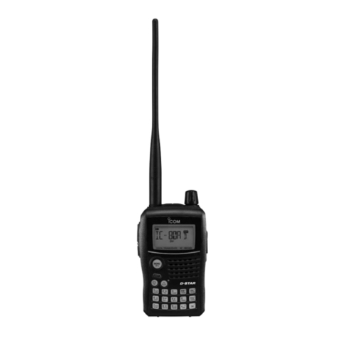
Icom IC-208H User manual

VHF/UHF FM TRANSCEIVER
i208H
SERVICE
MANUAL

INTRODUCTION
This service manual describes the latest service information
for the IC-208H VHF/UHF FM TRANSCEIVER at the time at
the time of publication.
DANGER
NEVER connect the transceiver to an AC outlet or to a DC
power supply that uses more than 16 V. This will ruin the
transceiver.
DO NOT expose the transceiver to rain, snow or any liquids.
DO NOT reverse the polarities of the power supply when con-
necting the transceiver.
DO NOT apply an RF signal of more than 20 dBm (100 mW)
to the antenna connector. This could damage the transceiv-
er’s front end.
ORDERING PARTS
Be sure to include the following four points when ordering
replacement parts:
1. 10-digit order numbers
2. Component part number and name
3. Equipment model name and unit name
4. Quantity required
<SAMPLE ORDER>
1140005990 S.IC
MB15A02PFV-1
IC-208H MAIN UNIT 5 pieces
8810009610 Screw FH M2.6×6 ZKIC-208H Bottom cover 10 pieces
Addresses are provided on the inside back cover for your
convenience.
REPAIR NOTES
1. Make sure a problem is internal before disassembling the
transceiver.
2. DO NOT open the transceiver until the transceiver is
disconnected from its power source.
3. DO NOT force any of the variable components. Turn
them slowly and smoothly.
4. DO NOT short any circuits or electronic parts. An insu-
lated tuning tool MUST be used for all adjustments.
5. DO NOT keep power ON for a long time when the trans-
ceiver is defective.
6. DO NOT transmit power into a signal generator or a
sweep generator.
7. ALWAYS connect a 50 dB to 60 dB attenuator between
the transceiver and a deviation meter or spectrum ana-
lyzer when using such test equipment.
8. READ the instructions of test equipment thoroughly
before connecting equipment to the transceiver.
To upgrade quality, any electrical or mechanical parts and
internal circuits are subject to change without notice or
obligation.
MODEL
IC-208H
VERSION
Taiwan
U.S.A.
Korea
Australia
Export
SYMBOL
TPE
USA
KOR
AUS
EXP

TABLE OF CONTENTS
SECTION 1 SPECIFICATIONS
SECTION 2 INSIDE VIEWS
SECTION 3 DISASSEMBLY INSTRUCTIONS
SECTION 4 CIRCUIT DESCRIPTION
4 - 1 RECEIVER CIRCUITS . . . . . . . . . . . . . . . . . . . . . . . . . . . . . . . . . . . . . . . . . . . . . . . . . . . . . . . . . . . .4 - 1
4 - 2 TRANSMITTER CIRCUITS . . . . . . . . . . . . . . . . . . . . . . . . . . . . . . . . . . . . . . . . . . . . . . . . . . . . . . . . .4 - 4
4 - 3 PLL CIRCUITS . . . . . . . . . . . . . . . . . . . . . . . . . . . . . . . . . . . . . . . . . . . . . . . . . . . . . . . . . . . . . . . . . .4 - 6
4 - 4 OTHER CIRCUITS . . . . . . . . . . . . . . . . . . . . . . . . . . . . . . . . . . . . . . . . . . . . . . . . . . . . . . . . . . . . . . .4 - 8
4 - 5 POWER SUPPLY CIRCUITS . . . . . . . . . . . . . . . . . . . . . . . . . . . . . . . . . . . . . . . . . . . . . . . . . . . . . . .4 - 8
4 - 6 PORT ALLOCATIONS . . . . . . . . . . . . . . . . . . . . . . . . . . . . . . . . . . . . . . . . . . . . . . . . . . . . . . . . . . . .4 - 9
SECTION 5 ADJUSTMENT PROCEDURES
5 - 1 PREPARATION . . . . . . . . . . . . . . . . . . . . . . . . . . . . . . . . . . . . . . . . . . . . . . . . . . . . . . . . . . . . . . . . . .5 - 1
5 - 2 SOFTWARE ADJUSTMENTS . . . . . . . . . . . . . . . . . . . . . . . . . . . . . . . . . . . . . . . . . . . . . . . . . . . . . . .5 - 3
SECTION 6 PARTS LIST
SECTION 7 MECHANICAL PARTS AND DISASSEMBLY
SECTION 8 SEMI-CONDUCTOR INFORMATION
SECTION 9 BOARD LAYOUTS
9 - 1 CONTROL UNIT . . . . . . . . . . . . . . . . . . . . . . . . . . . . . . . . . . . . . . . . . . . . . . . . . . . . . . . . . . . . . . . . .9 - 1
9 - 2 MAIN UNIT . . . . . . . . . . . . . . . . . . . . . . . . . . . . . . . . . . . . . . . . . . . . . . . . . . . . . . . . . . . . . . . . . . . . .9 - 3
9 - 3 VCO BOARD . . . . . . . . . . . . . . . . . . . . . . . . . . . . . . . . . . . . . . . . . . . . . . . . . . . . . . . . . . . . . . . . . . .9 - 5
SECTION 10 BLOCK DIAGRAM
SECTION 11 VOLTAGE DIAGRAMS
11 - 1 CONTROL UNIT . . . . . . . . . . . . . . . . . . . . . . . . . . . . . . . . . . . . . . . . . . . . . . . . . . . . . . . . . . . . . . . .11 - 1
11 - 2 MAIN UNIT . . . . . . . . . . . . . . . . . . . . . . . . . . . . . . . . . . . . . . . . . . . . . . . . . . . . . . . . . . . . . . . . . . . .11 - 2

1 - 1
SECTION 1 SPECIFICATIONS
All stated specifications are subject to change without notice or obligation.
MGENERAL
• Frequency range :
*1Guaranteed 144.000 – 146.000 MHz only, *2Guaranteed 144.000 – 148.000 MHz only,
*3Guaranteed 430.000 – 440.000 MHz only; *4Guaranteed 440.000 – 450.000 MHz only
*5Guaranteed 430.000 – 434.000 MHz, 435.000 – 438.000 MHz only; *6Not guaranteed range
• Mode : FM, AM (AM range is 118.0 – 135.995 MHz and Rx only for [USA] and [EXP].)
• Number of memory channel : 502 (including 2 call channels)
• Usable temperature range : –10˚C to +60˚C; +14˚F to +140˚F
• Frequency resolution : 5, 10, 12.5, 15, 20, 25, 30, 50, 100 and 200 kHz
• Scan mode : Full, Program, Priority, Memory channel, Bank, Skip and Tone
• Frequency stability : ±10 ppm (–10˚C to +60˚C; +14˚F to +140˚F)
• Power supply requirement : 13.8 V DC ±15 % (negative ground)
• Current drain (at 13.8 V DC) :
*1VHF only (except [KOR]), *2[TPE] only
• Antenna connector : SO-239 (50 Ω)
• DATA connector : Mini DIN 6 pin
• Dimensions : 141(W)×40(H)×185.4(D) mm; 59⁄16(W)×19⁄16(H)×79⁄32(D) inch (projections not included)
•Weight : 1.2 kg; 2 lb 10 oz
MTRANSMITTER
•Output power : VHF 55 W (50 W: [KOR], 25W: [TPE])/15 W/5 W (selectable)
UHF 50 W/15 W/5 W (selectable)
•Modulation system : Variable reactance frequency
•Maximum frequency deviation : ±5.0 kHz
•Spurious emissions : Less than –60 dB
•Microphone connector : 8-pin modular jack (600 Ω)
MRECEIVER
•Receive system : Double-conversion superheterodyne
•Intermediate frequency : 1st IF 46.05 MHz
2nd IF 450 kHz
•Sensitivity : Less than 0.18 µV (at 12 dB SINAD)
•Squelch sensitivity : Less than 0.13 µV (at threshold)
•Selectivity : More than 12 kHz/–6 dB (Wide); More than 6 kHz/–6 dB (Narrow)
Less than 30 kHz/–60 dB (Wide); Less than 20 kHz/–60 dB (Narrow)
•Spurious and image rejection : More than 60 dB
•Audio output power (at 13.8 V) : More than 2.0 W at 10% distortion with an 8 Ωload
•External speaker connector : 2-conductor 3.5(d) mm (1⁄8")/8 Ω
VERSION
[KOR]
[USA]
[AUS]
[TPE]
[EXP]
RX (MHz)
144.000–146.000, 430.000–440.000
118.000–173.995*2, 230.000–549.995*4
810.000–824.000*5, 849.000–869.000*5
894.000–999.990*5
118–173.995*2, 230.000–549.995*3,
810.000–999.990*6
144.000–146.000, 430.000–432.000
118–173.995*2, 230.000–549.995*3,
810.000–999.990*6
TX (MHz)
144.000–146.000*2, 430.000–440.000
144.000–148.000, 420.000–450.000*4
144.000–148.000, 420.000–450.000*3
144.000–146.000, 430.000–432.000
136.000–173.995*2, 400.000–478.995*3
VHF UHF
High: 55 W*1/50 W/25 W*212 A*1/11.5 A/8 A*211.5 A/8 A
TX Middle: 15 W (Approx.) 7.5 A
Low: 5 W (Approx) 5.5 A 5.0 A
RX Standby 0.8 A
Maximum output power 1.0 A

SECTION 2 INSIDE VIEWS
2 - 1
• CONTROL UNIT (TOP VIEW)
LCD back light
(DS22: CV1074)
Key back light
DS13-DS18,DS20: SML512MW
DS21: SML-020MYT
LCD back light
(DS22: CV1074)
Key back lights
DS13-DS18, DS20: SML512MW
DS21: SML-020MYT
• MAIN UNIT (TOP VIEW)
VCO board
EE PROM
(IC501: HN58X24128FPI)
AF amplifier
(IC510: LA4425A)
1st mixcer [VHF band]
(Q32: 3SK299)
1st mixcer [400M,800MHz band]
(IC12: µPC2757TB)
D/A converter
(IC11: M62352GP)
Ceramic band pass filter
FI1: CFWS450HT
FI2: CFWM450E
MAIN CPU
IC505
: HD6432143SA70FA[USA]
: HD6432143SA69FA except[USA]
VCO board
EEP ROM
(IC501: HN58X24128FPI)
AF amplifier
(IC510: LA4425A)
1st mixer [VHF band]
(Q32: 3SK299)
1st mixer [400M,800MHz band]
(IC12: µPC2757TB)
D/A converter
(IC11: M62352GP)
Ceramic bandpass filter
FI1: CFWS450HT
FI2: CFWM450E
MAIN CPU
IC505
: HD6432143SA70FA [USA]only
: HD6432143SA69FA except[USA]

• CONTROL UNIT (BOTTOM VIEW)
Color controller
(Q6,Q7: 2SC4116)
Control unit CPU
(IC6: HD6433842RB36H) Reset IC
(IC2: S-80945CLMC-G7F)
+5V regurator
IC5:TA78L05F
D4: MA8062
+8V regurator
Q1: 2SC4116
Q3: 2SA1734
D5: MA8068
Color controller
(Q6, Q7: 2SC4116)
Control unit CPU
(IC6: HD6433842RB36H) Reset IC
(IC2: S-80945CLMC-G7F)
+5V regulator
IC5:TA78L05F
D4: MA8062
+8V regulator
Q1: 2SC4116
Q3: 2SA1734
D5: MA8068
• MAIN UNIT (BOTTOM VIEW)
+8V regurator
(IC504:TA7808F)
+5V regurator
(IC503:TA7805F)
D/A converter
(IC4: M62363FP-650C)
IF IC
(IC8:TA31136FN)
APC controller
(IC15: NJM3404AV)
1st mixer [UHF band]
(Q35: 3SK299)
PA module [UHF band]
(IC14: S-AU82L) PA module [VHF band]
(IC13: S-AV32)
+8V regulator
(IC504:TA7808F)
+5V regulator
(IC503:TA7805F)
D/A converter
(IC4: M62363FP-650C)
FM IF IC
(IC8:TA31136FN)
APC controller
(IC15: NJM3404AV)
1st mixer [UHF band]
(Q35: 3SK299)
PA module [UHF band]
(IC14: S-AU82L) PA module [VHF band]
(IC13: S-AV32)
2 - 2

SECTION 3 DISASSEMBLY INSTRUCTIONS
• Removing the MAIN unit
➀Unscrew 4 screws A, and remove the cover.
➁Disconnect the cable Bfrom J505, and remove the
speaker.
➂Remove 2 sheets c.
➆Unscrew 8 screws G, and remove the MAIN unit.
J505J505
B
C
A
A
➃Unsolder 3 points D.
➄Disconnect the cable Efrom J1.
➅Unscrew 3 screws F, and remove the cover.
J1J1
FD
E
G
MAIN UNIT
3 - 1

• Removing the CONTROL unit
➀Remove 2 knobs A.➂Unscrew 2 screws C, and remove the LCD plate.
➃Remove the CONTROL unit.
A
➁Unscrew 2 screws B, and remove the cover.
B
C
CONTROL UNIT
3 - 2

4 - 1
4-1 RECEIVER CIRCUITS
4-1-1 DUPLEXER CIRCUIT (MAIN UNIT)
The transceiver has a duplexer (low-pass and high-pass fil-
ters) on the first stage from the antenna connector to sepa-
rate the signals into VHF, UHF and above 800 MHz signals.
The 2 of low-pass filters (L51, L52, L56, C295, C299 and
L45, L46, L49, C282, C285, C289) are for VHF signals, the
low-pass (L51, L52, L56, C295, C299) and high-pass (L47,
L50, C284, C288, C292, C586) filters are for UHF signals
and high-pass filter (L55, L58, C298, C302, C304) is for
above 800 MHz signals.
The separated signals are applied to each antenna switch-
ing circuits (except SHF signals).
4-1-2 ANTENNA SWITCHING CIRCUITS
(MAIN UNIT)
The antenna switching circuit functions as a low-pass filter
while receiving. However, its impedance becomes very high
while transmitting by turning ON diode (VHF: D47, D49,
D50; UHF: D46, D48, D51). Thus transmit signals are
blocked from entering the receiver circuits. The antenna
switching circuit employs a 1/4λtype diode switching sys-
tem.
SHF signals pass through the RX switching circuit (D44).
The passed signals are then applied to the each attenuator
circuits.
4-1-3 ATTENUATOR CIRCUITS (MAIN UNIT)
The attenuator circuit attenuates the signal strength to a
maximum of 10 dB to protect the RF amplifier from distortion
when excessively strong signals are received.
The signals from the antenna switching circuit pass through
the each attenuator circuit (for VHF is D49 and D50, for UHF
is D46 and D48, for SHF is D39).
The D/A converter outputs “ATT”signal (IC11, pin 6), and is
then applied to the attenuator controller circuit (Q44). The
circuit output attenuator control signals to each attenuator
circuits.
The attenuated signals are applied to the each RF circuits.
4-1-4 RF CIRCUITS (MAIN UNIT)
The RF circuit amplifies signals within the range of frequen-
cy coverage and filters out-of-band signals.
• VHF RF CIRCUIT (118 MHz–174 MHz)
The signals from the attenuator circuit pass through the tun-
able bandpass filter (D41, L40, L44, C273, C280). The fil-
tered signals are amplified at the VHF RF amplifier (Q38)
and are then enter another 3-stage tunable bandpass filter
(D22, D23, D29, L28, C171, C174, C176, C177, C181,
C185, C191, C198, C204, C208) to suppress unwanted sig-
nals and improve the selectivity. The filtered signals are
applied to the VHF 1st mixer circuit (Q32).
•UHF RF CIRCUIT (430 MHz–440 MHz)
The signals from the attenuator circuit are applied to the
UHF RX switching circuit (D42). The signals are amplified at
the UHF RF amplifier (Q39) and are then enter bandpass fil-
ter (FI4) to suppress unwanted signals. The filtered signals
are applied to the UHF 1st mixer circuit (Q35).
SECTION 4 CIRCUIT DESCRIPTION
LPF
VHF signals (118 174 MHz)
to the 2nd IF circuit
1st mixer (Q32)
Q38
Q39
Q36
Q37 Q41
Q40
1st mixer (Q35)
1st mixer (IC12)
Antenna
UHF signals (430 440 MHz)
LPF
T/R
SW
BPF
RF
AMP
BPF ATT
RX
SW
800M signals (810 1000 MHz)
HPF
RX
SW
BPF
RF
AMP
BPF ATT
RX
SW
RF
AMP
HPF
T/R
SW
RF
AMP
BPF
BPF
ATT
RX
SW
RX
SW
400M signals (230 550 MHz)
BPF
RF
AMP
RX
SW
RX
SW
RX
SW
RF
AMP
•RF CIRCUITS

4 - 2
•ABOVE 230 MHz RF CIRCUIT
(230 MHz–550 MHz, EXCEPT 430 MHZ–440 MHz)
The signals from the attenuator circuit pass through the tun-
able bandpass filter (D36, L37, L38, C242, C253, C261).
The filtered signals are amplified at the above 230MHz RF
amplifier (Q40) and are then enter another 2-stage tunable
bandpass filter (D25, D30, C205, C212) to suppress
unwanted signals and improve the selectivity. The filtered
signals are applied to the RF amplifier (Q36). The amplified
signals pass through the 400 MHz RX switching circuit
(D17), and then applied to the 400 MHz 1st mixer circuit
(IC12).
•ABOVE 800 MHz RF CIRCUIT (810 MHz–1000 MHz)
The signals from the attenuator circuit pass through the tun-
able bandpass filter (D37, L39, C243, C254, C260, C269).
The filtered signals are amplified at the above 800 MHz RF
amplifier (Q41) and are then enter another tunable band-
pass filter (D26, D31, L27, L31, C188, C197, C206, C213,
C223) to suppress unwanted signals and improve the selec-
tivity. The filtered signals are applied to the RF amplifier
(Q37). The amplified signals pass through the 400 MHz RX
switching circuit (D18), and then applied to the 1st mixer cir-
cuit (IC12) same as 400 MHz RF circuit.
The tunable bandpass filters (D11–D13, D15) employ var-
actor diodes to tune the center frequency of the RF pass-
band for wide bandwidth receiving and good image
response rejection.
4-1-5 VHF 1ST MIXER CIRCUIT (MAIN UNIT)
The 1st mixer circuit converts the received signal to a fixed
frequency of the 1st IF signal with a 1st LO frequency.
•VHF 1ST MIXER CIRCUIT
The signals from the VHF RF circuit are mixed with the 1st
LO signal at the 1st mixer circuit (Q32) to produce a 46.05
MHz 1st IF signal. The 1st IF signal passes through the RX
switching circuit (D8), and are then applied to the 1st IF cir-
cuit.
•UHF (430 MHz–440 MHz) 1ST MIXER CIRCUIT
The signals from the UHF RF circuit are mixed with the 1st
LO signal at the 1st mixer circuit (Q35) to produce a 46.05
MHz 1st IF signal. The 1st IF signal passes through the RX
switching circuit (D9), and are then applied to the 1st IF cir-
cuit.
•ABOVE 230 MHz (EXCEPT 430 MHz–440 MHz) 1ST
MIXER CIRCUIT
The signals from the above 230 MHz and above 800 MHz
RF circuit are mixed with the 1st LO signal at the 1st mixer
circuit (IC12) to produce a 46.05 MHz 1st IF signal. The 1st
IF signal passes through the RX switching circuit (D10), and
are then applied to the 1st IF circuit.
The output 46.05 MHz 1st IF signals from the each RX
switching circuits is applied to the crystal bandpass filter
(FI3), and then passed through the limiter circuit (D6). The
signal is amplified at the IF amplifier (Q18), and then applied
to the 2nd mixer circuit (IC8).
4-1-7 2ND IF AND DEMODULATOR CIRCUITS
(MAIN UNIT)
The 2nd mixer circuit converts the 1st IF signal to a 2nd IF
signal. A double superheterodyne system (which converts
receive signals twice) improves the image rejection ratio and
obtains stable receiver gain.
The FM IF IC (IC8) contains the 2nd local oscillator, 2nd
mixer, limiter amplifier, quadrature detector, and noise
detector circuits, etc.
The 1st IF signal from the IF amplifier is applied to the 2nd
mixer section of IC8 (pin 16), and is mixed with a 45.6 MHz
2nd LO signal generated by the reference oscillator circuit
(Q2, Q3, D1, X1) to produce a 450 kHz 2nd IF signal.
The 2nd IF signal from the 2nd mixer passes through the
ceramic bandpass filter (passes through FI2 during wide
channel spacing selection, or passes through FI1 during
narrow channel spacing selection), where unwanted signals
are suppressed. The ceramic filters (FI1, FI2) are switched
by IC9 and IC10 that is controlled by “WN_SEL”signal from
the MAIN CPU (IC505, pin 99).
The filtered signal is applied to the AM or FM detector circuit
separately.
W/N selector
FI2FI1
AM
DET
AM/FM
selector
2nd IF filter
450 kHz
Q13
Q16
IC9,
IC10,
Q21
Noise
detector
Q2,
Q7
Limiter
amp.
FM
detector
Active
filter
AF signals
("DET" signal)
R5
X2 Discriminator
RSSI
Mixer
45.6 MHz
1st IF from the
IF amplifier (Q18)
"RSSI" signal to the CPU
"SQL" signal to the CPU
875
BPF
32
3
1612 1411109
IC8
TA31136FN
X1
15.2 MHz
•2ND IF AND DEMODULATOR CIRCUITS

4 - 3
•IN CASE OF FM SIGNAL RECEIVING
The signal is then amplified at the limiter amplifier section
(IC5, pin 5) and applied to the FM detector section (X2, IC5,
pins 10, 11) for demodulation the 2nd IF signal into AF sig-
nals.
The FM detector circuit employs a quadrature detection
method (liner phase detection), which uses a ceramic dis-
criminator (X2) for phase delay to obtain a non-adjusting cir-
cuit. The detected signal from IC5 (pin 9) passes through the
AM/FM selector circuit (IC5, pins 7, 1), and is then applied
to the AF circuit.
•IN CASE OF AM SIGNAL RECEIVING
The signal is amplified at the amplifier (Q16), and is then
applied to the AM detector circuit (Q13) for demodulation the
2nd IF signal into AF signals.
The detected signal from Q13 passes through the AM/FM
selector circuit (IC5, pins 6, 1), and is then applied to the AF
circuit.
4-1-8 AF AMPLIFIER CIRCUIT (MAIN UNIT)
The AF amplifier circuit amplifies the detected signals to
drive a speaker. The AF circuit includes an AF mute circuit
for the squelch.
The detected AM or FM AF signals are applied to AF mute
circuit (Q14). The output signals pass through the low-pass
filter (Q5), and are then applied to the electric volume circuit
(IC508, pin 1). The signals are applied to the other AF mute
circuit (Q512). The signals are level adjusted at the volume
control IC (IC508), and are amplified at the AF power ampli-
fier (IC510, pin 1) after being passed through the other AF
mute circuit (Q512).
The output signal from IC510 (pin 4) drives the external or
internal speaker.
A part of signals from the AM/FM selector circuit (IC5, pin 1)
pass through low-pass filters.
When the signal passes through the low-pass filter (Q3), the
filtered signal is applied to the MAIN CPU (IC505, pin 39) via
the “DTCS_IN”signal to analyze the DTCS signal.
When the signal passes through the other low-pass filter
(C52, C53, R46, R52), the filtered signal is applied to the
MAIN CPU (IC505, pin 42) via the “WXALT”signal to detect
WX alert signal.
A part of signals from the AF mute circuit (Q14) is applied to
the 6-pins data jack as data signal via the “DATAOUT”sig-
nal.
4-1-9 SQUELCH CIRCUIT (MAIN UNIT)
•NOISE SQUELCH
A noise squelch circuit cuts out AF signals when no RF sig-
nals are received. By detecting noise components in the AF
signals, the squelch circuit switches the AF mute switch.
Some of the noise components in the AF signals from the
FM IF IC (IC8, pin 9) are passed through the active filter sec-
tion (IC8, pins 8, 7), and then applied to the noise detector
section. The detected noise signals are applied to the MAIN
CPU (IC505, pin 38) via the “SQL”line.
Even when the squelch is closed, the AF mute switch
(Q512) opens at the moment of emitting beep tone.
•TONE SQUELCH
The tone squelch circuit detects AF signals and opens the
squelch only when receiving a signal containing a matching
subaudible tone (CTCSS). When tone squelch is in use, and
a signal with a mismatched or no subaudible tone is
received, the tone squelch circuit mutes the AF signals even
when noise squelch is open.
A portion of the AF signals from the FM IF IC (IC8, pin 9)
passes through the low-pass filter (Q3) to remove AF (voice)
signals via the AM/FM AF selector (IC5, pins 7, 1), and is
then applied to the CTCSS decoder inside the CPU (IC505,
pin 39) via the “DTCS_IN”line to control the AF mute switch.
4-1-10 AGC CIRCUIT (MAIN UNIT)
The AGC (Automatic Gain Control) circuit reduces IF ampli-
fier gain to keep the audio output at a constant level. The
receiver gain is determined by the voltage on the AGC line
(Q13 collector).
FM IF IC
IC8
AM/FM
selector
AGC
AF signal
D19—D21,
D525
Antenna
IF
RF
RF
RF RF
RF RF
W/N selector
FI2FI1
AM
DET
RX
SW
RX
SW
RX
SW
2nd IF filter
450 kHz
IC9,
IC10,
Q21
Q13,
Q16
Q18
1st
mixer
•AGC CIRCUIT

4 - 4
The signal from the AM detector circuit (Q13) is detected at
the AGC detector circuit (D19–D21). When receiving strong
signals, the detected voltage increases and the AGC voltage
decreases via the AGC circuit. The AGC voltage is used for
the bias voltage of the receive switching PIN diodes to atten-
uate the received signals. Therefore, this transceiver keeps
the audio output at a constant level.
4-1-11 S-METER CIRCUIT (MAIN UNIT)
The S-meter circuit indicates the relative received signal
strength while receiving by utilizing the AGC voltage which
changes depending on the received signal strength.
The FM S-meter signal from the FM IF IC (IC8, pin 12) is
applied to the main CPU (IC505, pin 40) as an S-meter sig-
nal via the “RSSI”signal line.
The S-meter signal is applied to the sub CPU and is then
displayed on the LCD.
4-2 TRANSMITTER CIRCUITS
4-2-1 MICROPHONE AMPLIFIER CIRCUIT
(MAIN UNIT)
The microphone amplifier circuit amplifies audio signals
from the microphone to a level needed at the modulation cir-
cuit. The microphone amplifier circuit is commonly used for
both the VHF and UHF bands.
•AUDIO SIGNALS
The AF signals from the microphone are amplified at the
microphone amplifier (Q505, IC506), and are then applied to
the analog switch (IC509, pin 2). The signals from analog
switch (pin 1) are applied to the IDC amplifier (IC3A, pin 3)
via the “MODIN”line, and then pass through the low-pass fil-
ter (IC3D, pins 13, 14) to suppress unwanted components.
IC3A composes limiter amplifier and pre-emphasis circuits.
The signals are amplified at the buffer amplifier (IC3C, pins
9, 8), and are then applied to the D/A converter IC (IC4, pin
13) to adjust modulation level. The signals from the D/A con-
vertor (IC4, pin 23) pass through the reference controller
(D1, X1), and are then applied to the VHF or UHF modula-
tion circuits separately.
•DATA SIGNALS
The data signals from the 6-pins jack (J504, pin 1) pass
through the limiter circuit (D524) to limit the level.
When setting to 9600 bps mode, The signals pass through
the analog switch (IC509, pins 4, 3), and then pass through
the switch again (pins 9, 8). The signals are amplified at the
buffer amplifier (IC3c, pins 9, 8) via the “DATAMOD”line,
and are then applied to the same line as audio signals
(applied to the D/A converter IC’s pin 13).
When setting to 1200 bps mode, The signals pass through
the analog switch (IC509, pins 4, 3), and then pass through
the switch again (pins 10, 11). The signals are then applied
to the same line as “MODIN”(applied to the IDC amplifier;
IC3A, pin 3).
4-2-2 VHF MODULATION CIRCUIT
(MAIN UNIT AND VCO BOARD)
The modulation circuit modulates the VCO oscillating signal
(RF signal) using the microphone audio signals.
The audio or data signals from the reference controller (D1,
X1) are amplified at the buffer amplifier (Q2), and then pass
through the VHF PLL IC (IC1, pins 1,15) and VHF loop filter
(IC6, Q9, Q10, D4). The filtered signals are applied to the V-
VCO circuit (VCO board).
The signals change the reactance of D1 (VCO board) to
modulate the oscillated signal at the V-VCO circuit (VCO
board; Q3, D1, D2). The modulated signals are amplified at
the buffer amplifiers (VCO board; Q4, Q5), and then passed
through the Tx/Rx switching circuit (VCO board; D5) and
low-pass filter (L6, C32, C33). The filtered signals are
applied to the drive amplifier circuit on the MAIN unit.
Analog
SW
Amp
MIC
Antenna
IC506,
Q505 IC509 IC3A IC3D IC3C IC4
Q102,
Q103
Q2 IC1
IC2
X1
15.2 MHz
Buff
Buff
IDC
PLL IC Loop
filter
VCO
SW
VCO
SW
LPF
Buffs
Buffs
Pre
drive
Drive
PWR
LPF
SWR
DET
TX/RX
SW ATT
D/A
PLL IC Loop
filter
HPFLPF
LPF
VHF TX CIRCUIT
UHF TX CIRCUIT
HPFLPF
Pre
drive
Drive
PWR
LPF
SWR
DET
TX/RX
SW ATT
LPF
Q31Q34IC14
Q30Q33IC13
•TRANSMITTER CIRCUITS

4 - 5
4-2-3 VHF DRIVE AMPLIFIER CIRCUIT
(MAIN UNIT)
The drive amplifier circuit amplifies the VCO oscillating sig-
nal to a level needed at the power amplifier.
The RF signals from the low-pass filter (VCO board) pass
through the attenuator (R133, R134, R137), and are then
amplified at the pre-drive (Q30) and drive (Q33, D13) ampli-
fiers to obtain power that IC13 can operate. The amplified
signal is then applied to the RF power amplifier (IC1).
4-2-4 VHF POWER AMPLIFIER CIRCUIT
(MAIN UNIT)
The power amplifier circuit amplifies the driver signal to an
output power level.
IC13 is a power module which has amplification output
capabilities of about 55 W. The RF signal from the drive
amplifier (Q33) is applied to IC13 (pin 1).
The amplified signals from the power amplifier (IC13, pin 4)
pass through the low-pass filter (L22, C193, C189) and
SWR detector (D27, D33), antenna switching circuit (D45)
and other low-pass filter (L45, L46, L49, C279, C282, C285,
C289). The filtered signals are passed through the low-pass
filter (L51, L52, L56, C295, C299) to suppress unwanted sig-
nals, and are then applied to the antenna connector (CHAS-
SIS unit J2).
Control voltage for the power amplifier (IC13, pin 2) are con-
trolled by the APC circuit to protect the power module from
a mismatched condition as well as to stabilise the output
power.
4-2-5 VHF APC CIRCUIT (MAIN UNIT)
The APC circuit protects the power amplifier from a mis-
matched output load and stabilises transmit output power.
The SWR detector circuit (D27, D33, L29) detects forward
signals and reflection signals at D27 and D33 respectively.
The combined voltage is at a minimum level when the
antenna impedance is matched at 50 Ωand is increased
when it is mismatched.
The detected voltage is applied to the APC amplifier (IC15,
pin 6) and compared with a reference voltage which is sup-
plied from the CPU (IC505) as a “PCON_V”D/A control sig-
nal.
When antenna impedance is mismatched, the detected volt-
age exceeds the reference voltage. The output voltage of
the APC amplifier (IC15, pin 7) controls the bias voltage of
the power module (IC13) to reduce the output power via the
APC controller (IC15,).
4-2-6 UHF MODULATION CIRCUIT
(MAIN UNIT AND VCO BOARD)
The audio or data signals from the reference controller (D1,
X1) pass through the UHF PLL IC (IC2, pins 1,15) and UHF
loop filter (IC6, Q9, Q10, D4), and are then applied to the U-
VCO circuit (VCO board).
The signals change the reactance of D100 (VCO board) to
modulate the oscillated signal at the U-VCO circuit (VCO
board; Q101, D101, D102). The modulated signals are
amplified at the buffer amplifiers (VCO board; Q102, Q103),
and then passed through the Tx/Rx switching circuit (VCO
board; D103) and low-pass filter (L104, C122, C124). The fil-
tered signals are applied to the drive amplifier circuit on the
MAIN unit.
HV
to the VHF TX/RX switch
to the UHF TX/RX switch
APC controller
(IC15)
VHF SWR detector
IC13
L29
5
6
7
D27 D33
From the VHF
drive amplifier (Q33)
VHF power
amplifier
UHF power
amplifier
HV
IC14
D531
"PL_U" signal from the D/A
convertor (IC11, pin 19)
"PCON_V" signal from the D/A
convertor (IC11, pin 8)
"PCON_V" signal from the D/A
convertor (IC11, pin 9)
L30
3
2
1
D28 D34
From the UHF
drive amplifier (Q34)
LPF
LPF
UHF SWR detector
•APC CIRCUIT

4 - 6
4-2-7 UHF DRIVE AMPLIFIER CIRCUIT
(MAIN UNIT)
The RF signals from the low-pass filter (VCO board) pass
through the high-pass filter (L69, C119) and attenuator
(R135, R136, R138), and are then amplified at the pre-drive
(Q31) and drive (Q34, D14) amplifiers to obtain power that
IC14 can operate. The amplified signal is then applied to the
RF power amplifier (IC4).
4-2-8 UHF POWER AMPLIFIER CIRCUIT
(MAIN UNIT)
IC14 is a power module which has amplification output
capabilities of about 50 W. The RF signal from the drive
amplifier (Q34) is applied to IC14 (pin 1).
The amplified signals from the power amplifier (IC14, pin 4)
pass through the low-pass filter (L23, C190) and SWR
detector (D28, D34), antenna switching circuit (D40) and
high-pass filter (L47, L50, C284, C288, C292). The filtered
signals are passed through the low-pass filter (L51, L52,
L56, C295, C299) to suppress unwanted signals, and are
then applied to the antenna connector (CHASSIS unit J2).
Control voltage for the power amplifier (IC14, pin 2) are con-
trolled by the APC circuit to protect the power module from
a mismatched condition as well as to stabilise the output
power.
4-2-9 UHF APC CIRCUIT (MAIN UNIT)
The SWR detector circuit (D28, D34, L30) detects forward
signals and reflection signals at D28 and D34 respectively.
The combined voltage is at a minimum level when the
antenna impedance is matched at 50 Ωand is increased
when it is mismatched.
The detected voltage is applied to the APC amplifier (IC15,
pin 3) and compared with a reference voltage which is sup-
plied from the CPU (IC505) as a “PCON_U”D/A control sig-
nal.
When antenna impedance is mismatched, the detected volt-
age exceeds the reference voltage. The output voltage of
the APC amplifier (IC15, pin 1) controls the bias voltage of
the power module (IC14) to reduce the output power via the
APC controller (IC15, D531).
4-3 PLL CIRCUITS
4-3-1 GENERAL (MAIN UNIT)
A PLL circuit provides stable oscillation of the transmit fre-
quency and the receive local frequency. The PLL circuit
compares the phase of the divided VCO frequency to the
reference frequency. The PLL output frequency is controlled
by a crystal oscillator and the divided ratio of the program-
mable divider. IC1 and IC2 are dual PLL ICs that control both
VCO circuits for VHF and UHF.
4-3-2 VHF LOOP (VCO BOARD AND MAIN UNIT)
The generated signal at the V-VCO (Q3, D1, D2) enters the
PLL IC (MAIN unit; IC1, pin 8) via buffer-amplifiers (Q6, Q8)
and VCO switching circuit (D50) and is divided at the pro-
grammable divider section and is then applied to the phase
detector section.
The phase detector compares the input signal with a refer-
ence frequency, and then outputs the out-of-phase signal
(pulse-type signal) from pin 15 (MAIN unit).
The pulse-type signal is converted into DC voltage (lock
voltage) at the loop filter (MAIN unit; IC5, Q9, Q10, D4), and
then applied to the V-VCO to stabilise the oscillated fre-
quency.
Shift register
Prescaler
Phase
detector
Loop
filter
Programmable
counter
Programmable
divider
X2
15.2 MHz
45.6 MHz 2nd LO signal
to the FM IF IC (IC8, pin 3)
1
Buffer
Buffer
Buffer
9
10
11
PLLCK
PLLDATA
PLLSTB1
to the 1st mixer circuit
to the transmitter circuit
D5
D6
15 8
IC1 MB15A02PFV1
Q3, D1, D2
VHF VCO
16
Q4
Buffer
Q2
Buffer
Q7
D51
VCO
switch
VCO
switch
Q5
Q50
•VHF PLL CIRCUIT

4 - 7
4-3-3 UHF LOOP (VCO BOARD AND MAIN UNIT)
The generated signal at the U-VCO (Q101, D100, D101)
enters the PLL IC (MAIN unit; IC2, pin 8) via buffer-ampli-
fiers (Q102, Q50) and VCO switching circuit (D51) and is
divided at the programmable divider section and is then
applied to the phase detector section.
The phase detector compares the input signal with a refer-
ence frequency, and then outputs the out-of-phase signal
(pulse-type signal) from pin 15 (MAIN unit).
The pulse-type signal is converted into DC voltage (lock
voltage) at the loop filter (MAIN unit; IC7, Q11, Q12, D5),
and then applied to the U-VCO to stabilise the oscillated fre-
quency.
4-3-4 1ST LO CIRCUIT
(VCO BOARD AND MAIN UNIT)
The 1st VCO circuit contains a separate V-VCO (Q3, D1,
D2) and U-VCO (Q101, D100, D101).
•WHILE RECEIVING VHF BAND
The oscillated signal at the V-VCO circuit is amplified at the
buffer amplifier (Q4), and is then applied to the VCO switch-
ing circuit (D6). The signal passes through the attenuator
(C34, R24–R26) and low-pass filter (L7, L8, C36–C38), and
is then applied to the LO switching circuit.
(1) RECEIVING 118MHz–174 MHz
The signal is applied to the LO switching circuit (MAIN unit;
D528) as “V_RXLO”signal, and is applied to the 1st mixer
circuit (MAIN unit; Q32), then mixed with the 1st IF signal.
(2) RECEIVING 230 MHz–550 MHz
The signal is applied to the LO switching circuit (MAIN unit;
D15, D529, D530) as “V_RXLO”signal, and is applied to the
1st mixer circuit (MAIN unit; Q35), then mixed with the 1st IF
signal.
A portion of the RF signal from the buffer amplifier (Q4) is
amplified at the buffer amplifier (Q50), and is then fed back
to the PLL IC (MAIN unit; IC1, pin 8) as the comparison sig-
nal.
•WHILE RECEIVING UHF BAND OR 800 MHz BAND
The oscillated signal at the U-VCO circuit is amplified at the
buffer amplifiers (Q102, Q103), and is then applied to the
VCO switching circuit (for UHF band; D104, for 800 MHz;
D105).
While receiving UHF band, the signal passes through the
attenuator (C125, R117, R119, R120) and low-pass filter
(Q105, L7, L8, C36–C38), and is then applied to the VCO
switching circuit (D106).
While receiving 800 MHz band, the signal is doubled at the
doubler amplifier (Q104), and passes through the bandpass
filter (L108–L110, C127, C129, C132, C133, C135) and
attenuator (R127, R128). The signal is applied to the VCO
switching circuit (D107).
(1) RECEIVING UHF BAND
The signal is applied to the LO switching circuit (MAIN unit;
D9) as “U_RXLO”signal, and is applied to the 1st mixer cir-
cuit (MAIN unit; Q35), then mixed with the 1st IF signal.
(2) RECEIVING 800 MHz BAND
The signal is applied to the LO switching circuit (MAIN unit;
D10) as “U_RXLO”signal, and is applied to the 1st mixer cir-
cuit (MAIN unit; IC12, pin 6), then mixed with the 1st IF sig-
nal.
A portion of the RF signal from the buffer amplifier (Q102) is
amplified at the buffer amplifier (Q50) via the VCO switching
circuit (D51), and is then fed back to the PLL IC (MAIN unit;
IC1, pin 8) as the comparison signal.
Shift register
Prescaler
Phase
detector
Loop
filter
Programmable
counter
Programmable
divider
X2
15.3 MHz
1
Buffer
Buffer
Buffer
9
10
11
PLLCK
PLLDATA
PLLSTB2
to the 1st mixer circuit
D105
Q104
to the transmitter circuit
D103
D104
15 8
IC2 MB15A02PFV1
Q101, D100, D101
UHF VCO
16
Q102
D51
VCO
switch
VCO
switch
Q103
Q50
2
•UHF PLL CIRCUIT

4 - 8
4-4 OTHER CIRCUITS
4-4-1 SUB-CPU RESET CIRCUIT (CONTROL UNIT)
IC2 is the reset voltage detecting circuit. The output voltage
from the +5 regulator circuit (IC5) is applied to the VDD ter-
minal (IC2, pin 2). IC2 outputs “H”(high) signal to the sub-
CPU (IC6, pin 15) when the VDD terminal’s voltage is high-
er than detecting voltage.
IC6 employs the 8-bit CPU.
4-4-2 LCD DISPLAY CIRCUIT (CONTROL UNIT)
The transceiver’s LCD display employs 1/4 duty custom
LCD which displays frequency, S-meter, TX power level, etc.
The LCD display is controlled by the sub-CPU (IC6, pins
41–78) directly.
4-4-3 LCD AND KEY BACK LIGHT CIRCUIT
(CONTROL UNIT)
The sub-CPU (IC6) outputs +8 regulator circuit (Q1, Q3, D5)
control signal from pin 2. The voltage from +8 regulator cir-
cuit is applied to the key back light circuit (DS13–DS18,
DS20, DS23) and LCD back light circuit (DS22).
The back light color is also controlled by the sub-CPU via
the color control circuit (Q6, Q7). The back light has 3 colors
(Umber, Green and Yellow).
Description
The voltage from the external power supply via
the W501 (OPC-465).
The same voltage as the HV line which is con-
trolled by the VCC regulator circuit (Q501). The
circuit is controlled by the power switch controller
(Q502).
Common 8 V converted from the VCC line by the
+8 regulator circuit (IC504).
Transmit 8 V for VHF band which is the same
voltage as the 8V line controlled by the VT8 reg-
ulator circuit (Q19, Q22) using the “VTXC”line.
Transmit 8 V for UHF band which is the same
voltage as the 8V line controlled by the UT8 reg-
ulator circuit (Q20, Q23) using the “UTXC”line.
Common 5 V converted from the HV line by the
+5 regulator circuit (IC503).
Common 5 V converted from the 5V line by the
+5 regulator circuit(Q503, D504). The circuit is
controlled by the power switch controller (Q502).
Common 8 V converted from the 8 V line by the
+8 regulator circuit (Q4).
Common 8 V line which is selected by the
SEL_SW circuit (Q6, Q8). The voltage is applied
to the VHF VCO (VCO board; Q3, D1, D2) and
buffer amplifiers (VCO board; Q4, Q5).
Common 8 V line which is selected by the
SEL_SW circuit (Q6, Q8). The voltage is applied
to the UHF VCO (VCO board; Q101, D100,
D101) and buffer amplifiers (VCO board; Q102,
Q103).
Receive 5 V line converted from the 5VS line by
the R5 regulator circuit (Q24). The circuit is con-
trolled by the “R5CTRL”signal from the CPU
(IC505, pin 78).
Receive 5 V line for AM circuit converted from the
5VS line by the AM5 regulator circuit (Q25). The
circuit is controlled by the “AM”signal from the
CPU (IC505, pin 69).
Receive 5 V line for VHF circuit converted from
the 5VS line by the VHF_R5 regulator circuit
(Q26). The circuit is controlled by the “RXVHF”
signal from the CPU (IC505, pin 73).
Receive 5 V line for UHF circuit converted from
the 5VS line by the UHF_R5 regulator circuit
(Q27). The circuit is controlled by the “RXUHF”
signal from the CPU (IC505, pin 74).
Receive 5 V line for 400 MHz circuit converted
from the 5VS line by the 400_R5 regulator circuit
(Q28). The circuit is controlled by the “RX400”
signal from the CPU (IC505, pin 67).
Receive 5 V line for 800 MHz circuit converted
from the 5VS line by the 800_R5 regulator circuit
(Q29). The circuit is controlled by the “RX800”
signal from the CPU (IC505, pin 66).
Line
HV
VCC
8V
VT8
UT8
5V
5VS
VCO8
V_VCO8
U_VCO8
R5
AM5
VHF_R5
UHF_R5
400_R5
800_R5
4-5-2 MAIN UNIT VOLTAGE LINES
Description
Common 8 V converted from the HV line by the
+8 regulator circuit (Q1, Q3, D5). The output volt-
age is applied to the LCD back light (DS22) and
key back light (DS13–DS18, DS20, DS21, DS23)
circuits.
Common 5 V converted from the HV line by the
+5 regulator circuit (IC5, D4). The output voltage
is applied to the reset circuit (IC2) and buffer
amplifier (Q2).
Line
8V
CPU5V
4-5 POWER SUPPLY CIRCUITS
4-5-1 CONTROL UNIT VOLTAGE LINES

4 - 9
50
51
52
53
55
56
57
58
62
63
65
66
67
72
73
74
77
78
Input port for the cloning signal.
Outputs the data signal to the D/A
CONVERTER (IC11, pin 17).
Outputs the clock signal to the D/A
CONVERTER (IC11, pin 16).
Outputs the strobe signal to the D/A
CONVERTER (IC1, pin 15).
Outputs the AF mute control signal.
High : While AF signal is muting.
Outputs the strobe signal to the UHF
PLL IC (IC2, pin 11)
Outputs the strobe signal to the VHF
PLL IC (IC1, pin 11)
Outputs the detector circuit mute sig-
nal.
High : While the detector circuit is
muting.
Outputs microphone sensitivity control
signal.
High : The sensitivity is high.
Outputs the UHF VCO control signal.
High : The VCO circuit oscillates
320–999.99 MHz signal.
Outputs packet baud rate select sig-
nal.
Low : 9600 bps is selected.
Outputs the 800_R5 regulator (Q29)
control signal.
High : While receiving 630–999
MHz.
Outputs the 400_R5 regulator (Q28)
control signal.
High : While receiving 230–630
MHz.
Outputs the UHF_R5 regulator (Q27)
control signal.
High : While receiving 430–450
MHz.
Outputs the VHF_R5 regulator (Q26)
control signal.
High : While receiving 118–174
MHz.
Outputs modulation mute control sig-
nal to the VCO circuits.
High : While modulation is muting.
Outputs the microphone muting con-
trol signal.
Low : While the microphone is
muted.
Outputs the R5 regulator (Q24) control
signal.
Low : While receiving.
CLONE_IN
DA_DATA
DA_CK
DA_STB
AF_MUTE
PLLSTB2
PLLSTB1
DET_MUTE
MIC_SENS
U_VCO
1200_9600SEL
RX800
RX400
RXUHF
RXVHF
MMUTE
MIC_MUTE
R5CTRL
(MAIN unit; IC505)–Continued
Pin Port Description
number name
16
17
20
21
22
24
25
26
27
28
31
38
40
41
42
44
45
47
48
49
Outputs the transmit mute signal.
High : While transmit is muting.
Input port for the microphone PTT sig-
nal.
High : While PTT switch is pushed.
Outputs the UHF transmitting power
supply circuit control signal.
High : While transmitting (400–479
MHz)
Outputs the VHF transmitting power
supply circuit control signal.
High : While transmitting (136–174
MHz)
Outputs the DTCS filter select signal.
High : While the DTCS signal is
transmitting.
I/O port for the serial data to the EEP-
ROM (IC501, pin 5).
Outputs the clock signal to the EEP-
ROM (IC501, pin 6).
Input port for the packet [PTT] switch.
Low : While the packet [PTT] switch
is ON
Outputs the packet modulation muting
signal.
Low : While muting.
Input port for the HM-98’s data signal.
Input port for the connecting micro-
phone detect signal.
Low : While the HM-98 is connect-
ed.
Input port for the squelch level signal.
Input port for the RSSI signal from the
FM IF IC (IC8, pin 12) to detect receiv-
ing signal strength.
Input port for the transceiver’s internal
temperature signal.
Input port for the WX alert (1050 Hz)
signal.
Outputs DTMF, E-TONE and BEEP
signals.
Outputs CTCSS and DTCS signals.
Outputs the packet squelch control
signal.
High : While the squlech is opened.
Outputs the cooling fan control signal.
High : While the cooling fan is
worked.
Outputs the cloning signal.
4-6 PORT ALLOCATIONS
4-6-1 MAIN CPU PORT ALLOCATIONS
(MAIN UNIT; IC505)
TX_MUTE
MIC_PTT
UTXC
VTXC
DTCS_SEL
ES_DATA
ES_CK
P-PTT
P_MOD_MUTE
98_DATA
MIC_SEL
SQL
RSSI
TEMP
WXALT
DTMF
DTCS
P_SQL
FAN_CTRL
CLONE_OUT
Pin Port Description
number name

4 - 10
79
81
83
84
86–89
90
91
93–96
99
Outputs the VCO circuit select signal.
High : The VCO circuit oscillates
203.95–263.945 MHz signal.
Outputs the VHF VCO select signal.
High : The VHF VCO’s power supply
(Q6, Q8) is ON.
Outputs the PLL loop control signal.
Input port for the PLL unlock signal.
High : While the loop is unlocked.
Input ports for the initial matrix signals.
Outputs the PLL data signal to the PLL
ICs (IC1, IC2).
Outputs the PLL clock signal to the
PLL ICs (IC1, IC2).
Output the initial matrix strobe signals
Outputs the wide/narrow FM select
signal.
Low : While selected narrow FM.
VCO_SHIFT
V_VCO
PLLSW
UNLK
MATRIX_
IN1–IN4
PLLDATA
PLLCK
OUT1–OUT4
WN_SEL
Pin Port Description
number name
(MAIN unit; IC505)–Continued
2–4
5
6
7
8
9
12
13
18
Output the VHF bandpass filter track-
ing signals.
Outputs the UHF bandpass filter track-
ing signal.
Outputs the receiving attenuator con-
trol signal.
Outputs the bandpass filter shift con-
trol signal.
Low : While receiving 450–629.995
MHz.
Outputs the VHF output power control
signal.
Outputs the UHF output power control
signal.
Outputs the 800 MHz bandpass filter
tracking signal.
Outputs the reference frequency con-
trol signal.
Outputs the excess current detecting
signal.
TUNE_V1–V3
TUNE_U
ATT
BSHIFT
PCON_V
PCON_U
TUNE_8
REF_CON
REF_V
Pin Port Description
number name
4-6-2 D/A CONVERTER IC PORT ALLOCATIONS
(MAIN UNIT; IC11)
1
3
4
5
6
7
8
24
25
30
31
39–42
43–78
83
86
88
89
Input port for the [BAND] key.
Low : The [BAND] key is pushed.
Outputs the umber LED control signal.
High : The LED lights ON.
Input port for the [S.MW] key.
Low : The [S.MW] key is pushed.
Input port for the [TONE] key.
Low : The [TONE] key is pushed.
Input port for the [LOW] key.
Low : The [LOW] key is pushed.
Input port for the [MONI] key.
Low : The [MONI] key is pushed.
Input port for the [SET] key.
Low : The [SET] key is pushed.
Input port for the [M/CALL] key
Low : The [M/CALL] key is pushed.
Input port for the [V/MHz] key.
Low : The [V/MHz] key is pushed.
Input port for the main dial’s A phase
signal.
Input port for the main dial’s B phase
signal.
Output the common signals to the LCD
(DS1).
Output the segment signals to the LCD
(DS1).
Outputs the green LED control signal.
High : The LED lights ON.
Input port for the [PWR] key.
Low : The [PWR] key is pushed.
Input port for the [VOL] controller.
Input port for the [SQL] controller.
4-6-3 FRONT CPU PORT ALLOCATIONS
(CONTROL UNIT; IC6)
BAND
A_LED
SMW
TONE
LOW
MONI
SET
M/CALL
VMHz
DIAL_A
DIAL_B
COM4–COM1
SEG1–SEG36
G_LED
PWR
VOL
SQL
Pin Port Description
number name

5 - 1
5-1 PREPARATION
Need to enter the adjustment mode, and the JIG calble as shown the page 5-2 is required when adjusting the IC-208H.
■REQUIRED TEST EQUIPMENT
DC power supply
RF power meter
(terminated type)
Frequency counter
Standard signal
generator (SSG)
FM deviation meter
Oscilloscope
Audio generator
Attenuator
EQUIPMENT GREDE AND RANGE EQUIPMENT GREDE AND RENGE
SECTION 5 ADJUSTMENT PROCEDURES
Output voltage : 13.8 V DC
Current capacity : 12 A or more
Measuring range : 0.1–100 W
Frequency range : 1.8–600 MHz
Impedance : 50 Ω
SWR : Less than 1.2 : 1
Frequency range : 0.1–600 MHz
Frequency accuracy : ±1 ppm or better
Sensitivity : 100 mV or better
Frequency range : 0.1–1200 MHz
Output level : 0.1 µV–32 mV
(–127 to –17 dBm)
Frequency range : 0–600 MHz
Measuring range : 0 to ±5 kHz
Frequency range : DC–600 MHz
Measuring range : 0.01–10 V
Frequency range : 300–3000 Hz
Measuring range : 1–500 mV
Power attenuation : 50 or 60 dB
Capacity : 150 W or more
■ENTERING THE ADJUSTMENT MODE
qTurn the transceiver’s power OFF.
wConnect the JIG cable to the [MIC] jack.
ePush and hold the [SET] and [BAND] keys, and then turn power ON.
NOTE:Exiting from the adjustment mode when the transciever’s power is OFF.
■OPERATING ON THE ADJUSTMENT MODE
•Change the adjustment value : [DIAL]
•Verifying the adjustment value : [M/CALL] key
•Forward the adjustment item : [SET/LOCK] key
•Go back the adjustment item : [S.MW/MW] key
•Store the adjustment value in the memory : [BAND] key
CAUTION:Need to push the [BAND] key when storing the adjustment value in the memory. Otherwise, the transceiver is not
adjusted properly.
NOTE: *Need to adjust about manually adjustment items.
ADJUSTMENT ITEMS
Reference frequency’s temp. correction
Reference voltage
Protect time
Protect temperature
Cooling fan temperature
DTCS wave form
DTCS/CTCSS amplitude
*S-Meter
*Squelch level (Wide)
*Squelch level (Narrow)
DISPLAY
[Fr1]–[Fr8]
[rE–], [rE+]
[PT]
[PCV], [PCU]
[FT]
[DTA], [DTB]
[DT], [CT]
[SL]
[SqW]
[SqN]
ATTENTION!: DO NOT adjust following adjusment items (Because they are adjusted automatically when other
adjustment items are adjusted). Otherwise, the transceiver do not work properly. Refer to the next
page in detail.

5 - 2
‘‘CONNECTIONS
pin 6 (MIC)
pin 4 (PTT)
pin 7 (GND)
pin 2 (MICU/D)
pin 5 (MICE)
to the antenna connector
STANDARD SIGNAL GENERATOR
0.1 300 MHz
127 to 17 dBm (0.1 V to 32 mV)
RF POWER METER
50 , 1 80 W
FM DEVIATION
METER
ATTENUATOR
50 dB or 60 dB
POWER SUPPLY
13.8 V, 20 A or more
CAUTION!
DO NOT transmit
while an SSG is
connected to the
antenna connector. JIG CABLE INFORMATION
to the microphone connector
2.2 k
AUDIO GENERATOR
300 Hz to 3 kHz
ADJUSTMENT ITEM EXPLANATION
[Fr]
*[Fr1]*[Fr2]*[Fr3]*[Fr4]*[Fr5]*[Fr6]*[Fr7]*[Fr8]
[rE]
*[rE+][HP ]
[PM]
*[PCV]*[PCU]*[FT]*[DTA]*[DTB]*[DT]*[SL] *[CT]*[DT]*[CT]
[PP]
*[PT]
[HP+] [MP+] [LP+] [HP+] [MP+] [LP+]
[POH]
Starting item
[POM] [POL] [POH] [POM] [POL] [PL] [PV] [DE] [DT] [Tr] [SL]
[SqW][SqN]
*[SqW]*[SqN]
*[rE ]
[LP ][MP ][HP ][LP ][MP ]
*Not adjust items
DISPLAY
[Fr]
[rF]
[POH], [POM], [POL]
[PL]
[PV]
[DE]
[DT]
[Tr]
[SL]
[SqW]
[SqN]
*[Fr1], *[Fr2], *[Fr3], *[Fr4],
*[Fr5], *[Fr6], *[Fr7], *[Fr8]
ADJUSTMENT ITEMS
Reference frequency
Reference voltage
VHF/UHF output power
Transmit minimum voltage
Protect voltage
Frequency deviation
DTCS wave form
Tracking
S-Meter
Squelch level (Wide)
Squelch level (Narrow)
Reference frequency’s
temperature correction
DISPLAY
*[rE–], *[rE+]
[HP–], [HP+], [MP–],
[MP+], [LP–],[MP+]
[PM]
[PP]
*[PT]
*[PCV], *[PCU]
*[FT]
*[DTA], *[DTB]
*[DT], *[CT]
*[SL]
*[SqW]
*[SqN]
ADJUSTMENT ITEMS
Reference voltage
Temperature correction
Protect scale
Protect power
Protect time
Protect temperature
Cooling fan temperature
DTCS wave form
DTCS/CTCSS amplitude
S-Meter
Squelch level (Wide)
Squelch level (Narrow)
Other manuals for IC-208H
3
Table of contents
Other Icom Transceiver manuals

Icom
Icom IC-737A User manual

Icom
Icom IC-F4062S User manual

Icom
Icom IC-F50V User manual

Icom
Icom IC-41PRO Setup guide

Icom
Icom IC-F29DR2 User manual

Icom
Icom D-STAR ID-4100A User manual

Icom
Icom IC-701 User manual

Icom
Icom IC-V82 User manual

Icom
Icom iF3200DEX series User manual

Icom
Icom IC-U81T User manual