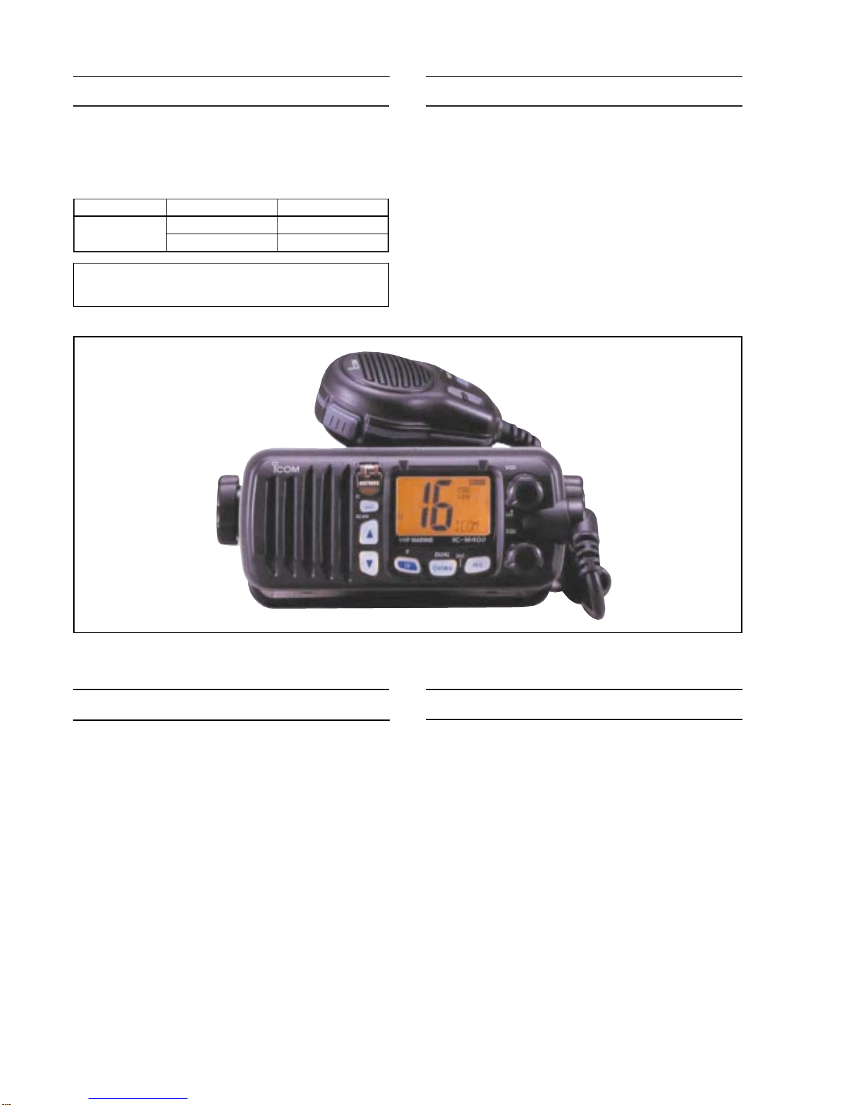
Icom IC-M402 User manual

SERVICE
MANUAL
VHF MARINE TRANSCEIVER
1-1-32, Kamiminami, Hirano-ku, Osaka, 547-0003, Japan S-13716IZ-CD
© 2001 Icom Inc.

INTRODUCTION DANGER
This service manual describes the latest service information
for the IC-M402 VHF MARINE TRANSCEIVER at the time of
publication.
2 versions of the IC-M402 have been designed. This service
manual covers each version.
MODEL
IC-M402
VERSION
USA
USA-1
SYNBOL
BLACK
WHITE
ORDERING PARTS
Be sure to include the following four points when ordering
replacement parts:
1. 10-digit order numbers
2. Component part number and name
3. Equipment model name and unit name
4. Quantity required
<SAMPLE ORDER>
1110003200 S.IC TA31136FN IC-M402 MAIN UNIT 5 pieces
8810006050 Screw Icom screw E7 IC-M402 Chassis 10 pieces
Addresses are provided on the inside back cover for your
convenience.
NEVER connect the transceiver to an AC outlet or to a DC
power supply that uses more than 16 V. This will ruin the
transceiver.
DO NOT expose the transceiver to rain, snow or any liquids.
DO NOT reverse the polarities of the power supply when
connecting the transceiver.
DO NOT apply an RF signal of more than 20 dBm (100mW)
to the antenna connector. This could damage the trans-
ceiver's front end.
REPAIR NOTES
1. Make sure a problem is internal before disassembling
the transceiver.
2. DO NOT open the transceiver until the transceiver is dis-
connected from its power source.
3. DO NOT force any of the variable components. Turn
them slowly and smoothly.
4. DO NOT short any circuits or electronic parts. An insulat-
ed turning tool MUST be used for all adjustments.
5. DO NOT keep power ON for a long time when the trans-
ceiver is defective.
6. DO NOT transmit power into a signal generator or a
sweep generator.
7. ALWAYS connect a 40 dB to 50 dB attenuator between
the transceiver and a deviation meter or spectrum ana-
lyzer when using such test equipment.
8. READ the instructions of test equipment thoroughly
before connecting equipment to the transceiver.
To upgrade quality, anyelectrical or mechanical parts and
internal circuits are subject to change without notice or
obligation.

SECTION 1 SPECIFICATIONS
SECTION 2 INSIDE VIEWS
2-1 IC-M402 . . . . . . . . . . . . . . . . . . . . . . . . . . . . . . . . . . . . . . . . . . . . . . . . . . . . . . . . . . . . . . . .2-1
2-2 HM-127 (OPTIONAL UNIT) . . . . . . . . . . . . . . . . . . . . . . . . . . . . . . . . . . . . . . . . . . . . . . . . . .2-2
SECTION 3 DISASSEMBLY INSTRUCTIONS
SECTION 4 CIRCUIT DESCRIPTION
4-1 RECEIVER CIRCUITS . . . . . . . . . . . . . . . . . . . . . . . . . . . . . . . . . . . . . . . . . . . . . . . . . . . . .4-1
4-2 TRANSMITTER CIRCUITS . . . . . . . . . . . . . . . . . . . . . . . . . . . . . . . . . . . . . . . . . . . . . . . . . .4-2
4-3 PLL CIRCUITS . . . . . . . . . . . . . . . . . . . . . . . . . . . . . . . . . . . . . . . . . . . . . . . . . . . . . . . . . . .4-3
4-4 DSC CIRCUITS . . . . . . . . . . . . . . . . . . . . . . . . . . . . . . . . . . . . . . . . . . . . . . . . . . . . . . . . . .4-4
4-5 LOGIC CIRCUITS . . . . . . . . . . . . . . . . . . . . . . . . . . . . . . . . . . . . . . . . . . . . . . . . . . . . . . . . .4-4
4-6 POWER SUPPLY CIRCUITS . . . . . . . . . . . . . . . . . . . . . . . . . . . . . . . . . . . . . . . . . . . . . . . .4-4
4-7 PORT ALLOCATIONS . . . . . . . . . . . . . . . . . . . . . . . . . . . . . . . . . . . . . . . . . . . . . . . . . . . . .4-5
SECTION 5 ADJUSTMENT PROCEDURES
5-1 PREPARATION . . . . . . . . . . . . . . . . . . . . . . . . . . . . . . . . . . . . . . . . . . . . . . . . . . . . . . . . . .5-1
5-2 PLL ADJUSTMENTS . . . . . . . . . . . . . . . . . . . . . . . . . . . . . . . . . . . . . . . . . . . . . . . . . . . . . .5-2
5-3 TRANSMITTER ADJUSTMENTS . . . . . . . . . . . . . . . . . . . . . . . . . . . . . . . . . . . . . . . . . . . . .5-3
5-4 RECEIVER ADJUSTMENTS . . . . . . . . . . . . . . . . . . . . . . . . . . . . . . . . . . . . . . . . . . . . . . . . .5-3
SECTION 6 PARTS LIST
6-1 IC-M402 . . . . . . . . . . . . . . . . . . . . . . . . . . . . . . . . . . . . . . . . . . . . . . . . . . . . . . . . . . . . . . . .6-1
6-2 HM-127 (OPTIONAL UNIT) . . . . . . . . . . . . . . . . . . . . . . . . . . . . . . . . . . . . . . . . . . . . . . . . . .6-6
6-3 HM-129 . . . . . . . . . . . . . . . . . . . . . . . . . . . . . . . . . . . . . . . . . . . . . . . . . . . . . . . . . . . . . . . .6-7
SECTION 7 MECHANICAL PARTS AND DISASSEMBLY
7-1 IC-M402 . . . . . . . . . . . . . . . . . . . . . . . . . . . . . . . . . . . . . . . . . . . . . . . . . . . . . . . . . . . . . . . .7-1
7-2 HM-129 . . . . . . . . . . . . . . . . . . . . . . . . . . . . . . . . . . . . . . . . . . . . . . . . . . . . . . . . . . . . . . . .7-3
7-2 HM-127 (OPTIONAL UNIT) . . . . . . . . . . . . . . . . . . . . . . . . . . . . . . . . . . . . . . . . . . . . . . . . . .7-3
SECTION 8 SEMI-CONDUCTOR INFORMATION
SECTION 9 BOARD LAYOUTS
9-1 VR-A BOARD . . . . . . . . . . . . . . . . . . . . . . . . . . . . . . . . . . . . . . . . . . . . . . . . . . . . . . . . . . . .9-1
9-2 VR-B BOARD . . . . . . . . . . . . . . . . . . . . . . . . . . . . . . . . . . . . . . . . . . . . . . . . . . . . . . . . . . . .9-1
9-3 HM-129 . . . . . . . . . . . . . . . . . . . . . . . . . . . . . . . . . . . . . . . . . . . . . . . . . . . . . . . . . . . . . . . .9-1
9-4 LOGIC BOARD . . . . . . . . . . . . . . . . . . . . . . . . . . . . . . . . . . . . . . . . . . . . . . . . . . . . . . . . . . .9-2
9-5 MAIN UNIT . . . . . . . . . . . . . . . . . . . . . . . . . . . . . . . . . . . . . . . . . . . . . . . . . . . . . . . . . . . . . .9-4
9-6 HM-127 (OPTIONAL UNIT) . . . . . . . . . . . . . . . . . . . . . . . . . . . . . . . . . . . . . . . . . . . . . . . . . .9-6
SECTION 10 BLOCK DIAGRAM
SECTION 11 VOLTAGE DIAGRAM
11-1 LOGIC BOARD . . . . . . . . . . . . . . . . . . . . . . . . . . . . . . . . . . . . . . . . . . . . . . . . . . . . . . . . . . .11-1
11-2 MAIN UNIT . . . . . . . . . . . . . . . . . . . . . . . . . . . . . . . . . . . . . . . . . . . . . . . . . . . . . . . . . . . . .11-2
11-3 HM-127 (OPTIONAL UNIT) . . . . . . . . . . . . . . . . . . . . . . . . . . . . . . . . . . . . . . . . . . . . . . . . . .11-3
11-4 HM-129 . . . . . . . . . . . . . . . . . . . . . . . . . . . . . . . . . . . . . . . . . . . . . . . . . . . . . . . . . . . . . . . .11-4
TABLE OF CONTENTS

1 - 1
SECTION 1 SPECIFICATIONS
‘‘GENERAL
• Frequency coverage : 156.025–157.425 MHz (Tx)
156.050–163.275 MHz (Rx)
• Mode : 16K0G3E (FM)
16K0G2B (DSC)
• Usable channels : All USA, international and Canadian channels
plus 10 weather channels
• Power supply requirement : 13.8 V DC ±10 % (negative ground)
• Usable temperature range : –20˚C to +60˚C; –4˚F to +140˚F
• Frequency stability : ±10 ppm (–20˚C to +60˚C; –4˚F to +140˚F)
• Current drain (at 13.8 V DC) : Transmit at 25 W 6.0 A (approx.)
Receive max. audio 1.2 A (approx.)
• Antenna impedance : 50 Ω(nominal)
• Input impedance (MIC) : 600 Ω
• Output impedance (Audio) : 4 Ω
• Dimensions (projections not included) : 153(W)×67(H)×141.6(D) mm; 6(W)×25⁄8(H)×53⁄5(D) in
• Weight : 900 g; 2 lb
‘‘TRANSMITTER
• Output power (at 13.8 V DC) : High 25 W
Low 1 W
• Modulation : Variable reactance frequency modulation
• Maximum frequency deviation : ±5.0 kHz
• Frequency error : ±10 ppm
• Spurious emissions : 70 dBc
• Adjacent channel power : 70 dB
• Residual modulation : 40 dB
• Audio harmonic distortion : Less than 10% at 60% deviation
• Audio frequency response : +1 dB to –3 dB of 6 dB octave from 300 Hz to 2500 Hz
‘‘RECEIVER
• Receive system : Double conversion superheterodyne system
• Intermediate frequencies : 1st 21.7 MHz
2nd 450 kHz
• Sensitivity : 0.32 µV at 12 dB SINAD
• Squelch sensitivity : 0.32 µV
• Adjacent channel selectivity : 70 dB
• Spurious response : 70 dB
• Intermodulation rejection ratio : 70 dB
• Hum and noise : 40 dB
• Audio output power (at 13.8 V DC) : 4.5 W typical at 10% distortion with an 4 Ωload
• Audio frequency responce : +1 dB to –3 dB of –6 dB octave from 300 Hz to 3000 Hz
Specifications are measured in accordance with TIA/EIA-603
All stated specifications are subject to change without notice or obligation.

1 - 2
*1Low power only, *2Momentary high power, *3Receive only
NOTE: Channels 3, 21, 23, 61, 64, 81, 82 and 83 CANNOT be used by the general public in USA waters.
CAN
21A
22A
23
24
25
26
27
28
60
61A
62A
64
64A
65A
66A*1
67
68
69
70*3
71
72
CAN
73
74
77*1
78A
79A
80A
81A
82A
83
83A
84
85
86
87
88
CAN
01
02
03
04A
05A
06
07A
08
09
10
11
12
13*1
14
15*1
16
17*1
18A
19A
20*1
21
‘‘VHF MARINE CHANNEL LIST
USA
01A
03A
05A
06
07A
08
09
10
11
12
13*2
14
15*2
16
17*1
18A
19A
20
20A
INT
01
02
03
04
05
06
07
08
09
10
11
12
13
14
15*1
16
17
18
19
20
21
Transmit
156.050
156.050
156.100
156.150
156.150
156.200
156.200
156.250
156.250
156.300
156.350
156.350
156.400
156.450
156.500
156.550
156.600
156.650
156.700
156.750
156.800
156.850
156.900
156.900
156.950
156.950
157.000
157.000
157.050
Receive
160.650
156.050
160.700
160.750
156.150
160.800
156.200
160.850
156.250
156.300
160.950
156.350
156.400
156.450
156.500
156.550
156.600
156.650
156.700
156.750
156.800
156.850
161.500
156.900
161.550
156.950
161.600
157.000
161.650
USA
21A
22A
23A
24
25
26
27
28
61A
63A
64A
65A
66A
67*2
68
69
70*3
71
72
INT
22
23
24
25
26
27
28
60
61
62
63
64
65
65A
66
66A
67
68
69
70*3
71
72
Transmit
157.050
157.100
157.100
157.150
157.150
157.200
157.250
157.300
157.350
157.400
156.025
156.075
156.075
156.125
156.125
156.175
156.175
156.225
156.225
156.275
156.275
156.325
156.325
156.375
156.425
156.475
156.525
156.575
156.625
Receive
157.050
161.700
157.100
161.750
157.150
161.800
161.850
161.900
161.950
162.000
160.625
160.675
156.075
160.725
156.125
160.775
156.175
160.825
156.225
160.875
156.275
160.925
156.325
156.375
156.425
156.475
156.525
156.575
156.625
USA
73
74
77*1
78A
79A
80A
81A
82A
83A
84
84A
85
85A
86
86A
87
87A
88
88A
INT
73
74
77
78
79
80
81
82
83
84
85
86
87
88
Transmit
156.675
156.725
156.875
156.925
156.925
156.975
156.975
157.025
157.025
157.075
157.075
157.125
157.125
157.175
157.175
157.225
157.225
157.275
157.275
157.325
157.325
157.375
157.375
157.425
157.425
Receive
156.675
156.725
156.875
161.525
156.925
161.575
156.975
161.625
157.025
161.675
157.075
161.725
157.125
161.775
157.175
161.825
157.225
161.875
157.275
161.925
157.325
161.975
157.375
162.025
157.425
Channel No. Frequency (MHz) Channel No. Frequency (MHz) Channel No. Frequency (MHz)
WX01
WX02
WX03
WX04
WX05
Transmit
Receive only
Receive only
Receive only
Receive only
Receive only
Receive
162.550
162.400
162.475
162.425
162.450
WX06
WX07
WX08
WX09
WX10
Transmit
Receive only
Receive only
Receive only
Receive only
Receive only
Receive
162.500
162.525
161.650
161.775
163.275
Frequency (MHz) Frequency (MHz)
Weather
channel Weather
channel
‘‘WX CHANNEL LIST

SECTION 2 INSIDE VIEWS
2 - 1
•MAIN UNIT
•FRONT UNIT
2-1 IC-M402
Reference oscillator
(X2: CR-659)
VCO circuit
FM IF IC
(IC1:TA31136FN)
2nd IF filter
(FI3: ALFY450E)
1st mixer
(Q1:3SK272)
Antenna switching circuit
1st IF filter
(FI1,FI2,: FL-310)
YGR amplifier
(Q11: 2SC3268)
DSC decoder
(IC6: NJM2211M)
AF power amplifier
(IC9: LA4425A) Pre-driver
(Q10: 2SC3775 3)
PLL IC
(IC2: MPD3140GS)
EEPROM
(IC2: HN58X2432TI)
VR-A board
VR-B board
MAIN MPU
(IC1: HD6473847RH)
System clock
(X1: CR-691)
Speaker
Reset IC
(IC6: NJM2211M)
LOGIC board

2 - 2
•TOP VIEW
•BOTTOM VIEW
2-2 HM-127 (OPTIONAL UNIT)
LCD
(DS1: A0119)
CPU
(IC1: µPD789405AGK-A30-9EU)
Data buffer circuit
System clock
(X1: CSTCC4.91MG)
8V regulator
(IC6: TA7808F)
Dimmer circuit
Reset IC
(IC7: S-80928ANMP)
MIC amplifier
(IC4: NJM2125F)
5V regulator
(IC5: TA78L05F) Volume IC
(IC3: M62429FP)
AF/MIC switch
(IC9: TC4W53FU)
AF amplifier
(IC2: TA7368F)

SECTION 3 DISASSEMBLY INSTRUCTIONS
3 - 1
•REMOVING THE CASE
1Unscrew 6 screws, A.
Note: When replacing the screw, 10–12 kg of torque MUST
be applied to ensure water resistance.
•REMOVING THE MAIN UNIT
1Unsolder DC cable (4 points) and antenna connector,
B (2 points), as shown below.
2Unscrew 2 screws, C, and 6 screws, D, to remove the
MAIN unit.
A
CB
D
2Slide the case free of the chassis in the direction of the
arrow.

4 - 1
4-1 RECEIVER CIRCUITS
4-1-1 ANTENNA SWITCHING CIRCUIT
(MAIN UNIT)
The antenna switching circuit functions as a low-pass filter
while receiving and as resonator circuit while transmitting.
The circuit does not allow transmit signals to enter receiver
circuits.
Received signals enter the MAIN unit from the antenna con-
nector and pass through the low-pass filter (L13, L14,
C106–C109, C111). The signals are then applied to the RF
circuit via the antenna switching circuit (D15, L15, C197,
C198).
4-1-2 RF CIRCUIT (MAIN UNIT)
The RF circuit amplifies signals within the range of frequen-
cy coverage and filters out-of-band signals.
The signals from the antenna switching circuit pass through
a tunable bandpass filter (D19, L16, L17, L19, L20,
C199–C204, C206–C210) where the object signals are led
to the RF amplifier circuit (Q27).
The amplified signals at Q7 are applied to the 3-stage tun-
able bandpass filter (D20, L21, L22, L24, L25, C213–C218,
C220–C224) to suppress unwanted signals and improve the
selectivity. The signals are then applied to the 1st mixer cir-
cuit.
4-1-3 1ST MIXER AND 1ST IF CIRCUITS
(MAIN UNIT)
The 1st mixer circuit converts the received signal to a fixed
frequency of the 1st IF signal with a 1st LO (VCO output) fre-
quency. By changing the 1st LO frequency, only the desired
frequency will be passed through two crystal filters at the
next stage of the mixer.
The signals from the RF circuit are mixed with the VCO sig-
nals at the 1st mixer circuit (Q1) to produce a 21.7 MHz 1st
IF signal.
The 1st IF signal is applied to two crystal filters (FI1, FI2) to
suppress out-of-band signals and is then amplified at the IF
amplifier (Q2). The amplified signal is applied to the 2nd
mixer circuit (IC1).
4-1-4 2ND IF AND DEMODULATOR CIRCUITS
(MAIN UNIT)
The 2nd mixer circuit converts the 1st IF signal to a 2nd IF
signal. A double superheterodyne system (which converts
receive signals twice) improves the image rejection ratio and
obtains stable receiver gain.
The FM IF IC (IC1) contains the 2nd local oscillator, 2nd
mixer, limiter amplifier, quadrature detector, and noise
detector circuits, etc.
The 1st IF signal from Q2 is applied to the 2nd mixer section
of IC1 (pin 16), and is mixed with a 21.25 MHz 2nd LO sig-
nal generated at the PLL circuit using the reference fre-
quency (21.25 MHz) to produce a 450 kHz 2nd IF signal.
The 2nd IF signal from IC1 (pin 3) is passed through the
ceramic filter (FI3), where unwanted signals are sup-
pressed, and is then applied to the 2nd IF (limiter) amplifier
in IC1 (pin 5). The signal is applied to the FM detector sec-
tion in IC1 for demodulation into AF signals.
The FM detector circuit employs a quadrature detection
method (linear phase detection), which uses a ceramic dis-
criminator (X1) for phase delay to obtain a non-adjusting cir-
cuit. The detected signal from IC1 (pin 9) is applied to theAF
circuit.
SECTION 4 CIRCUIT DESCRIPTION
Mixer
16
Limiter
amp.
2nd IF filter
450 kHz
PLL IC
IC3
X2
21.25 MHz
X1
(21.25 MHz)
RSSI
IC2 TA31136F
13 1st IF (21.7 MHz)
from the IF amplifier (Q2)
"SQL" signal to the CPU
(LOGIC board; IC1,pin 90)
11109
87 5 3
AF signal "DET"
R5
Squelch level
adjustment pot
(R16)
217 16
Active
filter
FI2
Noise
detector
FM
detector
C25
C26
C24
C28
R20
R18
R17
C27
R15
R21
C20
R19
R14
• 2ND IF AND DEMODULATOR CIRCUITS

4 - 2
4-1-5 AF AMPLIFIER CIRCUIT
(MAIN AND FRONT UNITS)
The AF amplifier circuit amplifies the detected signals to
drive a speaker. The AF circuit includes an AF mute circuit
for the squelch.
AF signals from IC1 (pin 9) are applied to the de-emphasis
circuit (R101, C140). The de-emphasis circuit is an integrat-
ed circuit with frequency characteristic of –6 dB/octave.
The integrated signals pass through the high-pass filter
(Q21, R96–R100, C138, C139) to suppress unwanted lower
noise signals.
The filtered signals are applied to theAF mute circuit (IC5A),
and then passes through the [VOLUME] control (VR-A
board; R1) via the “VOL1” signal. The signals are applied to
the AF power amplifier (IC9, pin 1). The output signal from
IC9 (pin4) drives the internal (external) speaker.
4-1-6 SQUELCH CIRCUIT
(MAIN UNIT AND LOGIC BOARD)
Asquelch circuit cuts outAF signals when no RF signals are
received. By detecting noise components in the AF signals,
the squelch circuit switches the AF mute switch.
A portion of the AF signals from the FM IF IC (IC1, pin 9)
pass through the squelch adjustment pot (R16), and are
then applied to the active filter section (IC1, pin 8). The
active filter section amplifies and filters noise components.
The filtered signals are applied to the noise detector section
and output from pin 14 as the “SQL” signal. The “SQL” sig-
nal is applied to the CPU (LOGIC board; IC1, pin 90). The
CPU analyzes the noise condition and outputs the “RMUM”,
“RMUTS” signals to toggle the AF mute switches (IC5A,
IC5B).
4-1-7 WEATHER ALERT DECODER CIRCUIT
(MAIN UNIT AND LOGIC BOARD)
When the weather alert function is activated and a 1050 Hz
alert tone from an NOAA weather radio broadcast is
received, the IC-M402 emits beep tones and indicates flash-
ing “ALT” on the display to inform of an emergency weather
report on the air.
AF signals from the FM IF IC (IC1, pin 9) pass through the
low-pass filter (Q28) via the “DET” signal, and are then
applied to A/D port of the CPU (LOGIC board; IC1, pin 88)
as “WXDEC” signal. The CPU has the tone decoder func-
tion. When a 1050 Hz signal is detected by software decode,
the CPU (LOGIC unit; IC1) controls beep tones and the
“ALT” indicator.
4-2 TRANSMITTER CIRCUITS
4-2-1 MICROPHONE AMPLIFIER CIRCUIT
(MAIN UNIT)
The microphone amplifier circuit amplifies audio signals with
+6 dB/octave pre-emphasis from the microphone to a level
needed at the modulation circuit.
The AF signals from the microphone are amplified at the
microphone amplifier (IC7B) via the analog switch (IC4A, pin
1). A capacitor (C159) and resistor (R121) are connected to
the amplifier to obtain the pre-emphasis characteristics.
The amplified signals are applied to the IDC amplifier (IC7C,
pin 9) and are passed through the splatter filter (IC7D) to
suppress unwanted 3 kHz or higher signals. The filtered sig-
nals are then applied to the modulation circuit.
4-2-2 MODULATION CIRCUIT (MAIN UNIT)
The modulation circuit modulates the VCO oscillating signal
(RF signal) using the microphone audio signals.
Audio signals from the splatter filter (IC7D) pass through the
frequency deviation adjustment pot (R138) and are then
applied to the modulation circuit (D2, D3, D4) to change the
reactance of D2, D3, D4 and modulate the oscillated signal
at the VCO (Q5, Q6).
4-2-3 DRIVE AMPLIFIER CIRCUIT (MAIN UNIT)
The drive amplifier circuit amplifies the VCO oscillating sig-
nal to a level needed at the power amplifier.
The VCO output is buffer-amplified by Q7 and Q9, and is
then applied to the Tx/Rx switch (D6). The transmit signal
from the Tx/Rx switch is amplified to the pre-drive (Q10) and
YGR (Q11) amplifiers to obtain an approximate 300 mW sig-
nal level. The amplified signal is then applied to the RF
power amplifier (IC3).
4-2-4 POWER AMPLIFIER CIRCUIT (MAIN UNIT)
The power amplifier circuit amplifies the driver signal to an
output power level.
IC3 is a power module which has amplification output capa-
bilities of about 35 W with 300 mW input. The output from
IC3 (pin 4) is passed through the antenna switching circuit
(D10) and is then applied to the antenna connector via the
low-pass filter.
AF
MUTE HPF
IC9
External SP
Internal SP
(LOGIC board)
HVS
PWR
AMP
"DET" signal from the
FM IF IC (IC1, pin 9)
de-emphasis
circuit
R101
C140
(VR-A board)
• AF AMPLIFIER CIRCUIT

4 - 3
4-2-5 APC CIRCUIT (MAIN UNIT)
The APC circuit stabilizes transmit output power.
The RF output signal from the power amplifier (IC3) is
detected at the power detector circuit (D8, D9, L12) and is
then applied to one of the differential amplifier inputs (Q15,
pin 5) via the High/Low control circuit (R71, Q16). The
applied voltage controls the differential amplifier output
(Q15, pin 2) and the bias voltage control (Q12). Thus the
APC circuit maintains a constant output power.
4-3 PLL CIRCUITS
4-3-1 GENERAL
The PLL circuit provides stable oscillation of the transmit fre-
quency and receive 1st LO frequency. The PLL circuit com-
pares the phase of the divided VCO frequency to the refer-
ence frequency. The PLLoutput frequency is controlled by a
crystal oscillator and the divided ratio of the programmable
divider.
IC2 on the MAIN unit is a dual PLL IC which controls both
VCO circuits for Tx and Rx, and contains a prescaler, pro-
grammable counter, programmable divider, phase detector,
charge pump, etc.
The PLL circuit , using a one chip PLL IC (MAIN unit; IC2),
directly generates the transmit frequency and receive 1st IF
frequency with VCOs. The PLL sets the divided ratio based
on serial data from the CPU on the LOGIC unit and com-
pares the phases of VCO signals with the reference oscilla-
tor frequency. The PLL IC detects the out-of-step phase and
output from pins 8 for Tx and Rx. The reference frequency
(21.25 MHz) is oscillated at X2 (MAIN unit).
4-3-2 TX AND RX LOOP (MAIN UNIT)
The generated signal at the VCO (Q4, Q5, Q6, D1–D4)
enters the PLL IC (IC2, pin 2) and is divided at the pro-
grammable divider section and is then applied to the phase
detector section.
The phase detector compares the input signal with a refer-
ence frequency, and then outputs the out-of-phase signal
(pulse-type signal) from pin 8.
The pulse-type signal is converted into DC voltage (lock
voltage) at the loop filter (R29–R31, R41, C41, C42, C50,
C51), and is then applied to varactor diodes (D3, D4) of the
VCO to stabilize the oscillated frequency. The lock voltage
from the loop filter is amplified at the buffer amplifier (Q7)
and then applied to the RF circuit.
T5
D8 D9
L12
"TMUT" signal from the CPU
(LOGIC board; IC1, pin 83)
HV
1
23
4
HI/LO
"TXDET" signal to the CPU
(LOGIC board; IC1, pin 92)
Q12 Q15
Q14
Q16
C93
R69
R70
Q11
YGR
amp.
RF signal
from PLL to antenna
RF detector
circuit
APC control circuit
Power module
IC3
R74
R73
R71
Shift register
Prescaler
Phase
detector
Loop
filter
Programmable
counter
Programmable
divider
X2
21.25 MHz
21.25 MHz signal to the
FM IF IC (IC1, pin 2)
VCO
Buffer
Buffer
Buffer Q9
Q8
Q7
3
4
5PSTB
IC2 (PLL IC)
PCK
PDATA
to transmitter circuit
to 1st mixer circuit
D6
D5
17
16
82
Q4 Q6, D1 D4
• APC CIRCUIT
• PLL CIRCUIT

4 - 4
4-3-4 VCO CIRCUIT (MAIN UNIT)
The VCO outputs from Q4–Q6 are buffer-amplified at the
buffer amplifiers (Q7 and Q9), and are then sent to theTx/Rx
switch (D5 and D6). The receive LO signal is applied to the
1st mixer circuit (Q1) through a low-pass filter, and the trans-
mit signal is applied to the pre-drive amplifier (Q10). A por-
tion of the VCO output is reapplied to the PLL IC (IC2, pin 2)
via the buffer amplifier (Q8).
4-4 DSC CIRCUITS
4-4-1 DSC ENCODE CIRCUIT
(LOGIC BOARD AND MAIN UNIT)
The DSC signal created at CPU (IC1), is passed through the
buffer amplifier (Q8), and applied to the D/A convertor
(R55–R73) to convert into the analog signal. The analog sig-
nal passes through the low-pass filter (MAIN unit; IC7D),
and is then applied to the VCO circuit to modulate the DSC
signal.
4-4-2 DSC DECODE CIRCUIT
(MAIN UNIT AND LOGIC BOARD)
The AF signal from the FM IF IC (IC1, pin 9) are filtered at
the low-pass filter (Q28) to suppress unwanted higher noise
signals. The filtered signals are converted analog signals
into digital signals at the DSC decoder IC (IC6), and are then
applied to the CPU (LOGIC board; IC1, pin 18).
4-5 LOGIC CIRCUITS (LOGIC BOARD)
• CPU
IC1 is an 8 bit signal chip micro-computer and contains LCD
driver, serial I/O, timer, A/D converter, programmable I/O,
ROM and RAM.
• SYSTEM CLOCK CIRCUIT
X1 is a ceramic oscillator and ocillate 9.8304 MHz system
clock for the CPU (IC1).
• RESET CIRCUIT
IC6 is a reset IC. When turn power ON, IC6 outputs a reset
signal (“LOW” pulse) to the CPU (IC1, pin 15) via the “RES”
line.
• LOW BATTERY DETECTOR
HVS voltage is divided by R74, R75 and is applied to the low
battery detector section in the CPU (IC1, pin 91) via the
“LBAT” line.
• DIMMER CIRCUIT
CPU (IC1), Q2, Q3 and Q4 are dimmer circuit and control
the 4 steps the LCD backlight (DS3–DS8).
4-6 POWER SUPPLY CIRCUITS
LINE
HV
HVS
VCC
5V
T5
R5
DESCRIPTION
The voltage from the connected DC power sup-
ply.
Same voltage as the HV line which is passed
through the [PWR] switch (VR-A board; R1).
Same voltage as the HVS line. The voltage is
applied to the optional microphone (HM-127).
Common 5 V converted from the HVS line at the
5V regulator circuit (MAIN unit; IC8).
Transmit 5 V controlled by the 5V control circuit
(MAIN unit; Q24, Q25) using the SEND signal
from CPU (LOGIC board; IC1). The controlled
voltage is applied to the transmitter circuit.
Receive 5 V controlled by the R5 control circuit
(MAIN unit; Q22, Q23) using the RCV circuit
from CPU (LOGIC board; IC1). The controlled
voltage is applied to the receiver circuit.

4 - 5
Pin Port Description
number name Pin Port Description
number name
1
2
3
5
6
7
8
16
17
18
20
21
22
23
27
28
29
31
83
84
88
89
90
91
CONT1
CONT2
BEEP
CH16
CHWX
H/L
DSDEC
PCK
PSTB
PDATA
ICFC
BPLVL
ECK
EDA
HI/LO
RRXD
RRXD
BPFV
TMUT
NMEAI
WXDEC
SQLV
SQL
LBAT
Outputs control signal for the LCD
contrast.
Outputs beep audio signal.
Input port for the CH16 switch.
Low: While CH16 switch is pushed.
Input port for the CHWX switch.
Low: While CHWX switch is pushed.
Input port for the H/L switch.
Low: While H/L switch is pushed.
Input port for ATIS/DSC decode sig-
nal.
Outputs clock signal to the PLL IC
(MAIN unit; IC2, pin 4).
Outputs strobe signals to the PLL IC
(MAIN unit; IC2, pin 3).
Outputs data signals to the PLL IC
(MAIN unit; IC2, pin 5).
Outputs control signal to swtich NMEA
or ICF3 (Optional unit; HM-127).
Outputs beep volume control signal.
Low: Beep audio is maximum.
Outputs clock signal for the EEPROM
(IC2, pin 6).
I/O port for the EEPROM data signals.
Output port for RF output power (High
or Low) select signal.
Input port for the communication data
from HM-127.
Outputs communication data to HM-
127.
Outputs bandpass filter select signals.
Low: Receiving more than 160 MHz.
High:Receiving less than 160 MHz.
Outputs transmit mute signal.
High:While transmitting.
Input port for GGA and NMEA data.
Input port for WX alert signal.
Input port for the squelch volume
level.
Input port from the FM IF IC (MAIN
unit; IC1) for the squelch operation.
Input port for the connected power
supply voltage detection (low battery
indicator).
92
93
94
95
96
97
98
99
Input port for TX LED control signal.
Input port for the smart mic functions.
2.02 V: [UP] is pushed.
3.00 V: [DN]] is pushed.
3.84 V: [16/9] is pushed.
Input port for the PTT switch from HM-
129.
Low: While PTT is pushed.
Input port for the DTRS switch.
Low: While DISTRESS switch is
pushed.
Input port for the DSC switch.
Low: While DSC switch is pushed.
Input port for the UP switch.
Low: While UP switch is pushed.
Input port for the DOWN switch.
Low: While DOWN switch is pushed.
Input port for the PLL unlock signal.
Low: While PLL is locked.
TXDET
KEYM
PTT
DTRS
DSC
UP
DOWN
UNLK
4-7 PORT ALLOCATIONS
4-7-1 CPU (LOGIC BOARD; IC1)
CONT1
0
1
CONT2
0
1
CONTRAST
LIGHT
DEEP
Pin Port Description
number name
4
5
6
7
11
12
13
14
RMUTM
RMUTS
PTTM
PTTS
MMUTE
SMUTE
SEND
RCV
Outputs the AF mute swtich (MAIN
unit; IC5) control signal for main body.
Low: While squelched
Outputs the AF mute swtich (MAIN
unit; IC5) control signal for the option-
al remote microphone (HM-127).
Low: While squelched
Outputs main microphone (HM-129)
select signal to the analog swtich
(IC4) while intercom operation.
Outputs optional microphone (HM-
127) select signal to the analog swtich
(IC4) while intercom operation.
Outputs select signal for the speaker
of the main microphone (HM-129) to
the analog swtich (IC5) while intercom
operation.
Outputs select signal for the speaker
of the optional microphone (HM-127)
to the analog swtich (IC5) while inter-
com operation.
Outputs the T5 regulator (MAIN unit;
Q24, Q25) control signal.
High:While transmitting
Outputs the R5 regulator (MAIN unit;
Q22, Q23) control signal.
High:While receiving.
4-7-2 I/O EXPANDER IC (LOGIC BOARD; IC3)

5 - 1
SECTION 5 ADJUSTMENT PROCEDURES
5-1 PREPARATION
■REQUIRED TEST EQUIPMENT
EQUIPMENT
DC power supply
RF power meter
(terminated type)
Frequency counter
FM deviation meter
DC voltmeter
Digital multi-meter
Distortion meter
GRADE AND RANGE
Output voltage : 13.8 V DC
Current capacity : 10 A or more
Measuring range : 1–50 W
Frequency range : 100–300 MHz
Impedance : 50 Ω
SWR : Less than 1.2 : 1
Frequency range : 0.1–300 MHz
Frequency accuracy: ±1 ppm or better
Sensitivity : 100 mV or better
Frequency range : 30–300 MHz
Measuring range : 0 to ±10 kHz
Input impedance : 50 kΩ/V DC or better
Input impedance : 10 MΩ/V DC or better
Frequency range : 1 kHz ±10 %
Measuring range : 1–100 %
EQUIPMENT
Audio generator
Standard signal
generator (SSG)
Oscilloscope
AC millivoltmeter
External speaker
Attenuator
Dummy load
GRADE AND RANGE
Frequency range : 300–3000 Hz
Measuring range : 1–500 mV
Frequency range : 0.1–300 MHz
Output level : 0.1 µV–32 mV
(–127 to –17 dBm)
Frequency range : DC–20 MHz
Measuring range : 0.01–20 V
Measuring range : 10 mV–10 V
Input impedance : 4 Ω
Capacity : 5 W or more
Power attenuation : 40 or 50 dB
Capacity : 50 W or more
Resistance : 50 Ω
Capacity : 100 W or more
‘‘CONNECTIONS
to the antenna connector
to DC cable
Standard signal
generator
17 to 125 dBm
(32 mV to 0.13 V)
CAUTION:
DO NOT transmit while SSG is
connected to the antenna connector.
DC power supply
13.8 V /15 A
Frequency
counter
FM deviation
meter
Attenuator
40 dB or 50 dB
+
to EXT Speaker
Red cap
(EXT SP jack)
Red line
Black line
RF power meter
50 / 1 50 W
Distortion meter
Speaker

5 - 2
5-2 PLL ADJUSTMENTS
LOCK
VOLTAGE
REFERENCE
FREQUENCY
ADJUSTMENT
ADJUSTMENT ADJUSTMENT CONDITION MEASUREMENT VALUE POINT
UNIT LOCATION UNIT ADJUST
1
2
1
• Operating channel : ch16
• Receiving
• Operating channel : ch16
• Output power : Low
• Transmitting
• Operating channel : ch16
• Output power : Low
• Connect an RF power meter or a
50 Ωdummy load to the antenna
connector.
• Transmitting
MAIN
Rear
Panel
Connect a digital
multi-meter or oscil-
loscope to the
check point CP1.
Loosely couple the
frequency counter
to the antenna con-
nector.
1.8 V
1.6 V
156.8000 MHz MAIN
Verify
C36
C36
Reference frequency
adjustment
CP1
PLL lock voltage
check point

5 - 3
5-4 RECEIVER ADJUSTMENTS
SENSITIVITY
SQUELCH
• Operating channel : ch16
• [SQUELCH] control:
Max. counterclockwise
• Connect an SSG to the antenna
connector and set as:
Frequency : 156.800 MHz
Level : 100 µV*
(–67 dBm)
Modulation : 1 kHz
Deviation : ±3.5 kHz
• Receiving
• Operating channel : ch16
• [SQUELCH] control:
Max. counterclockwise
• Connect an SSG to the antenna
connector and set as:
Frequency : 156.800 MHz
Level : 0.22 µV*
(–120 dBm)
Modulation : 1 kHz
Deviation : ±3.5 kHz
• Receiving
ADJUSTMENT
ADJUSTMENT ADJUSTMENT CONDITION MEASUREMENT VALUE POINT
UNIT LOCATION UNIT ADJUST
1
1
MAIN
MAIN
Connect the distor-
tion meter to the
[EXT SP] jack with a
4 Ωload.
Connect a DC volt-
meter to the check
point CP2.
Less than 0.32 µV
1.0 V MAIN
Verify
R16,
*This output level of a standard signal generator (SSG) is indicated as SSG’s open circuit.
5-3 TRANSMITTER ADJUSTMENTS
OUTPUT
POWER
FREQUENCY
DEVIATION
ADJUSTMENT
ADJUSTMENT ADJUSTMENT CONDITION MEASUREMENT VALUE POINT
UNIT LOCATION UNIT ADJUST
1
1
• Operating channel : ch16
• Output power : High
• Transmitting
• Operating channel : ch16
• Output power : Low
• Connect an audio generator to J4
(pin 3) on the MAIN unit with an
AC millivoltmeter and set as:
Frequency : 1 kHz
Level : 45 mV
• Set an FM deviation meter as:
HPF : OFF
LPF : 20 kHz
De-emphasis : OFF
Detector : (P–P)/2
• Transmitting
Rear
Panel
Rear
Panel
Connect an RF
power meter to the
antenna connector.
Connect an FM
deviation meter to
the antenna con-
nector through an
attenuator.
26 W
±4.3 kHz
MAIN
MAIN
R71
R138

5 - 4
+
+
J2
R71
Output power
adjustment
[PTT]
4
1
r
q
R138
Frequency deviation
adjustment
AC millivoltmeter
2 200 mV
Audio generator
300 Hz to 3 kHz
R16
Squelch level
adjustment
CP2
Squelch level
check point

[LOGIC BOARD]
IC1 1140009410 S.IC HD6433847RA29H (FX-2438A)
IC2 1130009680 S.IC HN58X2432TI
IC3 1130007570 S.IC BU4094BCFV-E2
IC4 1130005290 S.IC TC74HC14AF
IC5 1130006080 S.IC TC74HC02AF (TP1)
IC6 1130009110 S.IC S-80942ANMP-DD6-T2
IC7 1170000350 S.IC PC357N6T
Q1 1590000720 S.TRANSISTOR DTA144EUA T106
Q2 1530002850 S.TRANSISTOR 2SC4116-BL (TE85R)
Q3 1520000460 S.TRANSISTOR 2SB1132 T100 R
Q4 1530002850 S.TRANSISTOR 2SC4116-BL (TE85R)
Q5 1530002060 S.TRANSISTOR 2SC4081 T107 R
Q6 1590000680 S.TRANSISTOR DTC114EUA T106
Q7 1510000510 S.TRANSISTOR 2SA1576A T106R
Q8 1560000810 S.FET 2SK1069-4-TL
Q9 1590001330 S.TRANSISTOR DTA114EUA T106
Q10 1560000810 S.FET 2SK1069-4-TL
Q11 1560000810 S.FET 2SK1069-4-TL
D1 1750000550 S.DIODE 1SS355 TE-17
D2 1750000550 S.DIODE 1SS355 TE-17
X1 6050011090 S.XTAL CR-691 (9.8304 MHz)
R1 7030003680 S.RESISTOR ERJ3GEYJ 104 V (100 kΩ)
R2 7030003680 S.RESISTOR ERJ3GEYJ 104 V (100 kΩ)
R3 7030003680 S.RESISTOR ERJ3GEYJ 104 V (100 kΩ)
R4 7030003680 S.RESISTOR ERJ3GEYJ 104 V (100 kΩ)
R5 7030003430 S.RESISTOR ERJ3GEYJ 821 V (820 Ω)
R6 7030003430 S.RESISTOR ERJ3GEYJ 821 V (820 Ω)
R7 7030003800 S.RESISTOR ERJ3GEYJ 105 V (1 MΩ)
R8 7030003560 S.RESISTOR ERJ3GEYJ 103 V (10 kΩ)
R9 7030003620 S.RESISTOR ERJ3GEYJ 333 V (33 kΩ)
R10 7030003250 S.RESISTOR ERJ3GEYJ 270 V (27 Ω)
R11 7030003250 S.RESISTOR ERJ3GEYJ 270 V (27 Ω)
R12 7030003570 S.RESISTOR ERJ3GEYJ 123 V (12 kΩ)
R13 7030003500 S.RESISTOR ERJ3GEYJ 332 V (3.3 kΩ)
R14 7030003440 S.RESISTOR ERJ3GEYJ 102 V (1 kΩ)
R15 7030003630 S.RESISTOR ERJ3GEYJ 393 V (39 kΩ)
R16 7030003640 S.RESISTOR ERJ3GEYJ 473 V (47 kΩ)
R17 7030003560 S.RESISTOR ERJ3GEYJ 103 V (10 kΩ)
R18 7030003560 S.RESISTOR ERJ3GEYJ 103 V (10 kΩ)
R19 7030003560 S.RESISTOR ERJ3GEYJ 103 V (10 kΩ)
R20 7030003590 S.RESISTOR ERJ3GEYJ 183 V (18 kΩ)
R21 7030003590 S.RESISTOR ERJ3GEYJ 183 V (18 kΩ)
R22 7030003590 S.RESISTOR ERJ3GEYJ 183 V (18 kΩ)
R26 7030003380 S.RESISTOR ERJ3GEYJ 331 V (330 Ω)
R34 7030003400 S.RESISTOR ERJ3GEYJ 471 V (470 Ω)
R35 7030003540 S.RESISTOR ERJ3GEYJ 682 V (6.8 kΩ)
R36 7030003520 S.RESISTOR ERJ3GEYJ 472 V (4.7 kΩ)
R39 7030003640 S.RESISTOR ERJ3GEYJ 473 V (47 kΩ)
R41 7030003440 S.RESISTOR ERJ3GEYJ 102 V (1 kΩ)
R42 7030003640 S.RESISTOR ERJ3GEYJ 473 V (47 kΩ)
R43 7030003440 S.RESISTOR ERJ3GEYJ 102 V (1 kΩ)
R44 7030003630 S.RESISTOR ERJ3GEYJ 393 V (39 kΩ)
R45 7030003630 S.RESISTOR ERJ3GEYJ 393 V (39 kΩ)
R46 7030003550 S.RESISTOR ERJ3GEYJ 822 V (8.2 kΩ)
R47 7030003560 S.RESISTOR ERJ3GEYJ 103 V (10 kΩ)
R50 7030003580 S.RESISTOR ERJ3GEYJ 153 V (15 kΩ)
R51 7030003460 S.RESISTOR ERJ3GEYJ 152 V (1.5 kΩ)
R52 7030003560 S.RESISTOR ERJ3GEYJ 103 V (10 kΩ)
R53 7030003560 S.RESISTOR ERJ3GEYJ 103 V (10 kΩ)
R54 7030003560 S.RESISTOR ERJ3GEYJ 103 V (10 kΩ)
R55 7030003560 S.RESISTOR ERJ3GEYJ 103 V (10 kΩ)
R56 7030003560 S.RESISTOR ERJ3GEYJ 103 V (10 kΩ)
R57 7030003560 S.RESISTOR ERJ3GEYJ 103 V (10 kΩ)
R58 7030003560 S.RESISTOR ERJ3GEYJ 103 V (10 kΩ)
R59 7030003560 S.RESISTOR ERJ3GEYJ 103 V (10 kΩ)
R60 7030003560 S.RESISTOR ERJ3GEYJ 103 V (10 kΩ)
S.=Surface mount
R61 7030003560 S.RESISTOR ERJ3GEYJ 103 V (10 kΩ)
R62 7030004120 S.RESISTOR ERJ3GEYJ 203 V (20 kΩ)
R63 7030004120 S.RESISTOR ERJ3GEYJ 203 V (20 kΩ)
R64 7030004120 S.RESISTOR ERJ3GEYJ 203 V (20 kΩ)
R65 7030004120 S.RESISTOR ERJ3GEYJ 203 V (20 kΩ)
R66 7030004120 S.RESISTOR ERJ3GEYJ 203 V (20 kΩ)
R67 7030004120 S.RESISTOR ERJ3GEYJ 203 V (20 kΩ)
R68 7030004120 S.RESISTOR ERJ3GEYJ 203 V (20 kΩ)
R69 7030004120 S.RESISTOR ERJ3GEYJ 203 V (20 kΩ)
R70 7030003790 S.RESISTOR ERJ3GEYJ 824 V (820 kΩ)
R71 7030003490 S.RESISTOR ERJ3GEYJ 272 V (2.7 kΩ)
R72 7030004120 S.RESISTOR ERJ3GEYJ 203 V (20 kΩ)
R73 7030003720 S.RESISTOR ERJ3GEYJ 224 V (220 kΩ)
R74 7030003640 S.RESISTOR ERJ3GEYJ 473 V (47 kΩ)
R75 7030003700 S.RESISTOR ERJ3GEYJ 154 V (150 kΩ)
R76 7030003680 S.RESISTOR ERJ3GEYJ 104 V (100 kΩ)
R77 7030003280 S.RESISTOR ERJ3GEYJ 470 V (47 Ω)
R78 7030003680 S.RESISTOR ERJ3GEYJ 104 V (100 kΩ)
R79 7030003680 S.RESISTOR ERJ3GEYJ 104 V (100 kΩ)
R80 7030003560 S.RESISTOR ERJ3GEYJ 103 V (10 kΩ)
R81 7030003560 S.RESISTOR ERJ3GEYJ 103 V (10 kΩ)
R82 7030003680 S.RESISTOR ERJ3GEYJ 104 V (100 kΩ)
R83 7030003250 S.RESISTOR ERJ3GEYJ 270 V (27 Ω)
R84 7030003680 S.RESISTOR ERJ3GEYJ 104 V (100 kΩ)
R85 7030003500 S.RESISTOR ERJ3GEYJ 332 V (3.3 kΩ)
R86 7030003680 S.RESISTOR ERJ3GEYJ 104 V (100 kΩ)
R87 7030003680 S.RESISTOR ERJ3GEYJ 104 V (100 kΩ)
C1 4030006860 S.CERAMIC C1608 JB 1H 102K-T-A
C2 4030006860 S.CERAMIC C1608 JB 1H 102K-T-A
C3 4030006860 S.CERAMIC C1608 JB 1H 102K-T-A
C4 4030006850 S.CERAMIC C1608 JB 1H 471K-T-A
C5 4030006860 S.CERAMIC C1608 JB 1H 102K-T-A
C6 4030006850 S.CERAMIC C1608 JB 1H 471K-T-A
C7 4030006900 S.CERAMIC C1608 JB 1E 103K-T-A
C8 4510004630
S.ELECTROLYTIC
ECEV1CA100SR
C9 4030006880 S.CERAMIC C1608 JB 1H 472K-T-A
C10 4030008890 S.CERAMIC C1608 JB 1C 273K-T-A
C11 4030006900 S.CERAMIC C1608 JB 1E 103K-T-A
C12 4030006900 S.CERAMIC C1608 JB 1E 103K-T-A
C13 4030006900 S.CERAMIC C1608 JB 1E 103K-T-A
C14 4030006900 S.CERAMIC C1608 JB 1E 103K-T-A
C18 4030006900 S.CERAMIC C1608 JB 1E 103K-T-A
C20 4030006900 S.CERAMIC C1608 JB 1E 103K-T-A
C21 4030006860 S.CERAMIC C1608 JB 1H 102K-T-A
C22 4510004630
S.ELECTROLYTIC
ECEV1CA100SR
C23 4030006900 S.CERAMIC C1608 JB 1E 103K-T-A
C24 4030007060 S.CERAMIC C1608 CH 1H 270J-T-A
C25 4030006900 S.CERAMIC C1608 JB 1E 103K-T-A
C26 4030006900 S.CERAMIC C1608 JB 1E 103K-T-A
C27 4030006900 S.CERAMIC C1608 JB 1E 103K-T-A
C28 4030009650 S.CERAMIC C1608 CH 1H 240J-T-A
C29 4510005860
S.ELECTROLYTIC
ECEV1HA2R2SR
C30 4030006900 S.CERAMIC C1608 JB 1E 103K-T-A
C31 4030006900 S.CERAMIC C1608 JB 1E 103K-T-A
C32 4030006860 S.CERAMIC C1608 JB 1H 102K-T-A
J1 6510015540 S.CONNECTOR B4B-ZR-SM3-TF
J2 6510018960 S.CONNECTOR B2B-PH-SM3-TB
J3 6510018960 S.CONNECTOR B2B-PH-SM3-TB
J4 6510022470 S.CONNECTOR 40FLT-SM1-TB
DS1 5030001950 LCD TTR5341
DS3 5040002310 S.LED SML-311YTT86
DS4 5040002310 S.LED SML-311YTT86
DS5 5040002310 S.LED SML-311YTT86
DS6 5040002310 S.LED SML-311YTT86
DS7 5040002660 S.LED FY1101F-TR (LED)
DS8 5040002660 S.LED FY1101F-TR (LED)
6 - 1
SECTION 6 PARTS LIST
REF ORDER DESCRIPTION
NO. NO. REF ORDER DESCRIPTION
NO. NO.
6-1 IC-M402
[LOGIC BOARD]

[MAIN UNIT][LOGIC BOARD]
S.=Surface mount
EP1 0910053453 PCB B 5584C
EP2 8930054970 LCD CONTACT SRCN-2438-SP-N-W
R1 7210002350 VARIABLE TP96N97N15F-10KA-1301
W1 8900010510 CABLE OPC-1044
EP1 0910053462 PCB B 5585B
R1 7210002360 VARIABLE TP96N97-15F-10KB-1301
EP1 0910053472 PCB B 5586B
IC1 1110003200 S.IC TA31136FN (EL)
IC2 1130007610 S.IC µPD3140GS-E1 (DS8)
IC3 1150001540 IC M57710-A/SC-1302
IC4 1130008090 S.IC BU4066BCFV-E1
IC5 1130008090 S.IC BU4066BCFV-E1
IC6 1110003650 S.IC NJM2211M-TE1
IC7 1110002680 S.IC NJM2902M-T1
IC8 1180001070 S.IC TA7805F (TE16L)
IC9 1110003090 IC LA4425A
Q1 1580000660 S.FET 3SK272-(TX)
Q2 1530002360 S.TRANSISTOR 2SC2714-Y (TE85R)
Q3 1530002850 S.TRANSISTOR 2SC4116-BL (TE85R)
Q4 1590000430 S.TRANSISTOR DTC144EUA T106
Q5 1530002920 S.TRANSISTOR 2SC4226-T2 R25
Q6 1530002920 S.TRANSISTOR 2SC4226-T2 R25
Q7 1530002600 S.TRANSISTOR 2SC4215-O (TE85R)
Q8 1530002600 S.TRANSISTOR 2SC4215-O (TE85R)
Q9 1530002600 S.TRANSISTOR 2SC4215-O (TE85R)
Q10 1530002240 S.TRANSISTOR 2SC3775-3-TB
Q11 1530003710 S.TRANSISTOR 2SC3268 (TE12L)
Q12 1520000380 TRANSISTOR 2SB1143 S
Q14 1590000430 S.TRANSISTOR DTC144EUA T106
Q15 1590000670 S.TRANSISTOR FMW1 T148
Q16 1590000430 S.TRANSISTOR DTC144EUA T106
Q17 1540000550 S.TRANSISTOR 2SD1664 T100Q
Q18 1590000430 S.TRANSISTOR DTC144EUA T106
Q19 1590000720 S.TRANSISTOR DTA144EUA T106
Q20 1560000810 S.FET 2SK1069-4-TL
Q21 1530002850 S.TRANSISTOR 2SC4116-BL (TE85R)
Q22 1510000670 S.TRANSISTOR 2SA1588-GR (TE85R)
Q23 1590000430 S.TRANSISTOR DTC144EUA T106
Q24 1510000670 S.TRANSISTOR 2SA1588-GR (TE85R)
Q25 1590000430 S.TRANSISTOR DTC144EUA T106
Q26 1590000430 S.TRANSISTOR DTC144EUA T106
Q27 1530002920 S.TRANSISTOR 2SC4226-T2 R25
Q28 1530002850 S.TRANSISTOR 2SC4116-BL (TE85R)
D1 1790000620 S.DIODE MA77 (TX)
D2 1790000620 S.DIODE MA77 (TX)
D3 1720000370 S.VARICAP HVU350TRF
D4 1720000370 S.VARICAP HVU350TRF
D5 1790000620 S.DIODE MA77 (TX)
D6 1790000620 S.DIODE MA77 (TX)
D7 1750000550 S.DIODE 1SS355 TE-17
D8 1790000690 S.DIODE HSM88ASR-TR
D9 1790000690 S.DIODE HSM88ASR-TR
D10 1710001080 DIODE XB15A308
D11 1790000700 DIODE DSA3A1
D12 1750000550 S.DIODE 1SS355 TE-17
D14 1750000130 S.DIODE DA204U T107
D15 1710001080 DIODE XB15A308
D16 1790001210 S.DIODE 1SS375-TL
D19 1790000620 S.DIODE MA77 (TX)
D20 1790000620 S.DIODE MA77 (TX)
D21 1790000660 S.DIODE MA728 (TX)
FI1 2010002420 MONOLITH 21R15AB (FL-310)
FI2 2010002420 MONOLITH 21R15AB (FL-310)
FI3 2020001680 CERAMIC ALFY450E
X1 6070000210
S.DISCRIMINATOR
CDBCA450CX24
X2 6050010800 S.XTAL CR-659 (21.25 MHz)
L1 6200003050 S.COIL NL 322522T-R82J-3
L2 6200002410 S.COIL NL 252018T-056J
L3 6200002430 S.COIL NL 252018T-082J
L4 6200003090 S.COIL NL 322522T-2R7J-3
L5 6200008190 S.COIL 0.25-1.9-8TL 80N
L6 6200009180 S.COIL ELJRE R10J-F3
L7 6200009180 S.COIL ELJRE R10J-F3
L8 6200009180 S.COIL ELJRE R10J-F3
L9 6200002430 S.COIL NL 252018T-082J
L10 6200002430 S.COIL NL 252018T-082J
L11 6170000230 COIL LW-25
L12 6110001600 COIL LA-243
L13 6110001600 COIL LA-243
L14 6110001670 COIL LA-253
L15 6110001600 COIL LA-243
L16 6200007760 S.COIL LQN21A 82NJ04
L17 6200007760 S.COIL LQN21A 82NJ04
L19 6200007760 S.COIL LQN21A 82NJ04
L20 6200007760 S.COIL LQN21A 82NJ04
L21 6200007760 S.COIL LQN21A 82NJ04
L22 6200007760 S.COIL LQN21A 82NJ04
L24 6200007760 S.COIL LQN21A 82NJ04
L25 6200007760 S.COIL LQN21A 82NJ04
L26 6200004720 S.COIL MLF1608D R10K-T
L27 6200003550 S.COIL MLF1608A 4R7K-T
L28 6200009150 S.COIL ELJRE 82NJ-F3
L29 6200009170 S.COIL ELJRE 47NJ-F2
L30 6200002600 S.COIL NL 252018T-047J
L31 6200002600 S.COIL NL 252018T-047J
R3 7030003560 S.RESISTOR ERJ3GEYJ 103 V (10 kΩ)
R5 7030003560 S.RESISTOR ERJ3GEYJ 103 V (10 kΩ)
R6 7030003200 S.RESISTOR ERJ3GEYJ 100 V (10 Ω)
R7 7030003500 S.RESISTOR ERJ3GEYJ 332 V (3.3 kΩ)
R8 7030003480 S.RESISTOR ERJ3GEYJ 222 V (2.2 kΩ)
R9 7030003460 S.RESISTOR ERJ3GEYJ 152 V (1.5 kΩ)
R10 7030003460 S.RESISTOR ERJ3GEYJ 152 V (1.5 kΩ)
R11 7030003680 S.RESISTOR ERJ3GEYJ 104 V (100 kΩ)
R12 7030003460 S.RESISTOR ERJ3GEYJ 152 V (1.5 kΩ)
R13 7030003400 S.RESISTOR ERJ3GEYJ 471 V (470 Ω)
R14 7030003450 S.RESISTOR ERJ3GEYJ 122 V (1.2 kΩ)
R15 7030003400 S.RESISTOR ERJ3GEYJ 471 V (470 Ω)
R16 7310002760 S.TRIMMER RV-152 (RH03A3AJ4X0HA) 223
R17 7510001050 S.THERMISTOR NTCCM1608 4LH 333KC-T
R18 7030003620 S.RESISTOR ERJ3GEYJ 333 V (33 kΩ)
R19 7030003430 S.RESISTOR ERJ3GEYJ 821 V (820 Ω)
R20 7030003740 S.RESISTOR ERJ3GEYJ 334 V (330 kΩ)
R21 7030003390 S.RESISTOR ERJ3GEYJ 391 V (390 Ω)
R22 7030003460 S.RESISTOR ERJ3GEYJ 152 V (1.5 kΩ)
R25 7030003320 S.RESISTOR ERJ3GEYJ 101 V (100 Ω)
R26 7030003380 S.RESISTOR ERJ3GEYJ 331 V (330 Ω)
R27 7030003460 S.RESISTOR ERJ3GEYJ 152 V (1.5 kΩ)
6 - 2
REF ORDER DESCRIPTION
NO. NO. REF ORDER DESCRIPTION
NO. NO.
[VR-B BOARD]
REF ORDER DESCRIPTION
NO. NO.
[MAIN UNIT]
REF ORDER DESCRIPTION
NO. NO.
[VR-A BOARD]
REF ORDER DESCRIPTION
NO. NO.

S.=Surface mount
[MAIN UNIT][MAIN UNIT]
R28 7030003380 S.RESISTOR ERJ3GEYJ 331 V (330 Ω)
R29 7030003440 S.RESISTOR ERJ3GEYJ 102 V (1 kΩ)
R30 7030003200 S.RESISTOR ERJ3GEYJ 100 V (10 Ω)
R31 7030003480 S.RESISTOR ERJ3GEYJ 222 V (2.2 kΩ)
R32 7030003560 S.RESISTOR ERJ3GEYJ 103 V (10 kΩ)
R33 7030003440 S.RESISTOR ERJ3GEYJ 102 V (1 kΩ)
R34 7030003440 S.RESISTOR ERJ3GEYJ 102 V (1 kΩ)
R35 7030003640 S.RESISTOR ERJ3GEYJ 473 V (47 kΩ)
R36 7030003320 S.RESISTOR ERJ3GEYJ 101 V (100 Ω)
R37 7030003620 S.RESISTOR ERJ3GEYJ 333 V (33 kΩ)
R38 7030003680 S.RESISTOR ERJ3GEYJ 104 V (100 kΩ)
R39 7030003600 S.RESISTOR ERJ3GEYJ 223 V (22 kΩ)
R40 7030003470 S.RESISTOR ERJ3GEYJ 182 V (1.8 kΩ)
R41 7030003410 S.RESISTOR ERJ3GEYJ 561 V (560 Ω)
R42 7030003550 S.RESISTOR ERJ3GEYJ 822 V (8.2 kΩ)
R43 7030003550 S.RESISTOR ERJ3GEYJ 822 V (8.2 kΩ)
R44 7030003320 S.RESISTOR ERJ3GEYJ 101 V (100 Ω)
R45 7030003390 S.RESISTOR ERJ3GEYJ 391 V (390 Ω)
R46 7030003350 S.RESISTOR ERJ3GEYJ 181 V (180 Ω)
R47 7030003420 S.RESISTOR ERJ3GEYJ 681 V (680 Ω)
R48 7030003660 S.RESISTOR ERJ3GEYJ 683 V (68 kΩ)
R49 7030003400 S.RESISTOR ERJ3GEYJ 471 V (470 Ω)
R50 7030003660 S.RESISTOR ERJ3GEYJ 683 V (68 kΩ)
R51 7030003320 S.RESISTOR ERJ3GEYJ 101 V (100 Ω)
R52 7030003610 S.RESISTOR ERJ3GEYJ 273 V (27 kΩ)
R53 7030003440 S.RESISTOR ERJ3GEYJ 102 V (1 kΩ)
R54 7030003480 S.RESISTOR ERJ3GEYJ 222 V (2.2 kΩ)
R56 7030003520 S.RESISTOR ERJ3GEYJ 472 V (4.7 kΩ)
R57 7030003520 S.RESISTOR ERJ3GEYJ 472 V (4.7 kΩ)
R58 7030003320 S.RESISTOR ERJ3GEYJ 101 V (100 Ω)
R59 7030003200 S.RESISTOR ERJ3GEYJ 100 V (10 Ω)
R60 7030003440 S.RESISTOR ERJ3GEYJ 102 V (1 kΩ)
R61 7030003320 S.RESISTOR ERJ3GEYJ 101 V (100 Ω)
R62 7030003440 S.RESISTOR ERJ3GEYJ 102 V (1 kΩ)
R63 7030000960 S.RESISTOR MCR18EZHJ 33 Ω
R64 7030000960 S.RESISTOR MCR18EZHJ 33 Ω
R65 7030003640 S.RESISTOR ERJ3GEYJ 473 V (47 kΩ)
R66 7030003500 S.RESISTOR ERJ3GEYJ 332 V (3.3 kΩ)
R67 7030003480 S.RESISTOR ERJ3GEYJ 222 V (2.2 kΩ)
R68 7030003560 S.RESISTOR ERJ3GEYJ 103 V (10 kΩ)
R69 7030003360 S.RESISTOR ERJ3GEYJ 221 V (220 Ω)
R70 7030003560 S.RESISTOR ERJ3GEYJ 103 V (10 kΩ)
R71 7310002670 S.TRIMMER RV-143 (RH03A3AS2) 471
R73 7030003540 S.RESISTOR ERJ3GEYJ 682 V (6.8 kΩ)
R74 7030003680 S.RESISTOR ERJ3GEYJ 104 V (100 kΩ)
R75 7030000240 S.RESISTOR MCR10EZHJ 68 Ω(680)
R76 7030003400 S.RESISTOR ERJ3GEYJ 471 V (470 Ω)
R77 7030000240 S.RESISTOR MCR10EZHJ 68 Ω(680)
R78 7030003480 S.RESISTOR ERJ3GEYJ 222 V (2.2 kΩ)
R79 7030003480 S.RESISTOR ERJ3GEYJ 222 V (2.2 kΩ)
R80 7030003320 S.RESISTOR ERJ3GEYJ 101 V (100 Ω)
R81 7030003560 S.RESISTOR ERJ3GEYJ 103 V (10 kΩ)
R82 7030003490 S.RESISTOR ERJ3GEYJ 272 V (2.7 kΩ)
R83 7030003450 S.RESISTOR ERJ3GEYJ 122 V (1.2 kΩ)
R84 7030003550 S.RESISTOR ERJ3GEYJ 822 V (8.2 kΩ)
R85 7030003800 S.RESISTOR ERJ3GEYJ 105 V (1 MΩ)
R86 7030003800 S.RESISTOR ERJ3GEYJ 105 V (1 MΩ)
R87 7030003680 S.RESISTOR ERJ3GEYJ 104 V (100 kΩ)
R88 7030003680 S.RESISTOR ERJ3GEYJ 104 V (100 kΩ)
R89 7030003800 S.RESISTOR ERJ3GEYJ 105 V (1 MΩ)
R90 7030003800 S.RESISTOR ERJ3GEYJ 105 V (1 MΩ)
R91 7030003800 S.RESISTOR ERJ3GEYJ 105 V (1 MΩ)
R92 7030003440 S.RESISTOR ERJ3GEYJ 102 V (1 kΩ)
R93 7030003800 S.RESISTOR ERJ3GEYJ 105 V (1 MΩ)
R94 7030003800 S.RESISTOR ERJ3GEYJ 105 V (1 MΩ)
R95 7030003800 S.RESISTOR ERJ3GEYJ 105 V (1 MΩ)
R96 7030003490 S.RESISTOR ERJ3GEYJ 272 V (2.7 kΩ)
R97 7030003390 S.RESISTOR ERJ3GEYJ 391 V (390 Ω)
R98 7030003760 S.RESISTOR ERJ3GEYJ 474 V (470 kΩ)
R99 7030003700 S.RESISTOR ERJ3GEYJ 154 V (150 kΩ)
R100 7030003580 S.RESISTOR ERJ3GEYJ 153 V (15 kΩ)
R101 7030003580 S.RESISTOR ERJ3GEYJ 153 V (15 kΩ)
R102 7030003440 S.RESISTOR ERJ3GEYJ 102 V (1 kΩ)
R103 7030003280 S.RESISTOR ERJ3GEYJ 470 V (47 Ω)
R104 7030003590 S.RESISTOR ERJ3GEYJ 183 V (18 kΩ)
R105 7030003560 S.RESISTOR ERJ3GEYJ 103 V (10 kΩ)
R106 7030003620 S.RESISTOR ERJ3GEYJ 333 V (33 kΩ)
R107 7030003640 S.RESISTOR ERJ3GEYJ 473 V (47 kΩ)
R108 7030003760 S.RESISTOR ERJ3GEYJ 474 V (470 kΩ)
R109 7030003680 S.RESISTOR ERJ3GEYJ 104 V (100 kΩ)
R110 7030003630 S.RESISTOR ERJ3GEYJ 393 V (39 kΩ)
R111 7030003580 S.RESISTOR ERJ3GEYJ 153 V (15 kΩ)
R112 7030003480 S.RESISTOR ERJ3GEYJ 222 V (2.2 kΩ)
R113 7030003680 S.RESISTOR ERJ3GEYJ 104 V (100 kΩ)
R121 7030003480 S.RESISTOR ERJ3GEYJ 222 V (2.2 kΩ)
R122 7030003590 S.RESISTOR ERJ3GEYJ 183 V (18 kΩ)
R123 7030003650 S.RESISTOR ERJ3GEYJ 563 V (56 kΩ)
R124 7030003440 S.RESISTOR ERJ3GEYJ 102 V (1 kΩ)
R125 7030003540 S.RESISTOR ERJ3GEYJ 682 V (6.8 kΩ)
R126 7030003680 S.RESISTOR ERJ3GEYJ 104 V (100 kΩ)
R127 7030003770 S.RESISTOR ERJ3GEYJ 564 V (560 kΩ)
R128 7030003520 S.RESISTOR ERJ3GEYJ 472 V (4.7 kΩ)
R129 7030003610 S.RESISTOR ERJ3GEYJ 273 V (27 kΩ)
R130 7030003590 S.RESISTOR ERJ3GEYJ 183 V (18 kΩ)
R131 7030003670 S.RESISTOR ERJ3GEYJ 823 V (82 kΩ)
R132 7030003670 S.RESISTOR ERJ3GEYJ 823 V (82 kΩ)
R133 7030003670 S.RESISTOR ERJ3GEYJ 823 V (82 kΩ)
R134 7030003620 S.RESISTOR ERJ3GEYJ 333 V (33 kΩ)
R135 7510001150 S.THERMISTOR NTCCM1608 4BH 103KC
R136 7030003590 S.RESISTOR ERJ3GEYJ 183 V (18 kΩ)
R137 7030003580 S.RESISTOR ERJ3GEYJ 153 V (15 kΩ)
R138 7310002600 S.TRIMMER RV-110 (RH03A3AS4X0AA) 473
R139 7030003550 S.RESISTOR ERJ3GEYJ 822 V (8.2 kΩ)
R140 7030003200 S.RESISTOR ERJ3GEYJ 100 V (10 Ω)
R141 7030003550 S.RESISTOR ERJ3GEYJ 822 V (8.2 kΩ)
R142 7030003540 S.RESISTOR ERJ3GEYJ 682 V (6.8 kΩ)
R143 7030003540 S.RESISTOR ERJ3GEYJ 682 V (6.8 kΩ)
R144 7030001070 S.RESISTOR MCR50JZHJ 33 Ω(330)
R145 7030003560 S.RESISTOR ERJ3GEYJ 103 V (10 kΩ)
R146 7030003480 S.RESISTOR ERJ3GEYJ 222 V (2.2 kΩ)
R147 7030003560 S.RESISTOR ERJ3GEYJ 103 V (10 kΩ)
R148 7030003480 S.RESISTOR ERJ3GEYJ 222 V (2.2 kΩ)
R149 7030003580 S.RESISTOR ERJ3GEYJ 153 V (15 kΩ)
R150 7030003450 S.RESISTOR ERJ3GEYJ 122 V (1.2 kΩ)
R151 7030003600 S.RESISTOR ERJ3GEYJ 223 V (22 kΩ)
R152 7030003800 S.RESISTOR ERJ3GEYJ 105 V (1 MΩ)
R154 7030000100 S.RESISTOR MCR10EZHJ 4.7 Ω(4R7)
R155 7030003620 S.RESISTOR ERJ3GEYJ 333 V (33 kΩ)
R157 7030003280 S.RESISTOR ERJ3GEYJ 470 V (47 Ω)
R158 7030003240 S.RESISTOR ERJ3GEYJ 220 V (22 Ω)
R159 7030003440 S.RESISTOR ERJ3GEYJ 102 V (1 kΩ)
R160 7030003560 S.RESISTOR ERJ3GEYJ 103 V (10 kΩ)
R161 7030003560 S.RESISTOR ERJ3GEYJ 103 V (10 kΩ)
R162 7030003560 S.RESISTOR ERJ3GEYJ 103 V (10 kΩ)
R163 7030003440 S.RESISTOR ERJ3GEYJ 102 V (1 kΩ)
R165 7030003680 S.RESISTOR ERJ3GEYJ 104 V (100 kΩ)
R166 7030003680 S.RESISTOR ERJ3GEYJ 104 V (100 kΩ)
R167 7030003680 S.RESISTOR ERJ3GEYJ 104 V (100 kΩ)
R168 7030003680 S.RESISTOR ERJ3GEYJ 104 V (100 kΩ)
R169 7030003680 S.RESISTOR ERJ3GEYJ 104 V (100 kΩ)
R170 7030003680 S.RESISTOR ERJ3GEYJ 104 V (100 kΩ)
R183 7030003680 S.RESISTOR ERJ3GEYJ 104 V (100 kΩ)
R185 7030003560 S.RESISTOR ERJ3GEYJ 103 V (10 kΩ)
R186 7030003440 S.RESISTOR ERJ3GEYJ 102 V (1 kΩ)
R187 7030003440 S.RESISTOR ERJ3GEYJ 102 V (1 kΩ)
R188 7030003320 S.RESISTOR ERJ3GEYJ 101 V (100 Ω)
R190 7030003560 S.RESISTOR ERJ3GEYJ 103 V (10 kΩ)
R191 7030003560 S.RESISTOR ERJ3GEYJ 103 V (10 kΩ)
R192 7030003320 S.RESISTOR ERJ3GEYJ 101 V (100 Ω)
R193 7030003440 S.RESISTOR ERJ3GEYJ 102 V (1 kΩ)
R194 7030003440 S.RESISTOR ERJ3GEYJ 102 V (1 kΩ)
R195 7030003440 S.RESISTOR ERJ3GEYJ 102 V (1 kΩ)
R196 7030003440 S.RESISTOR ERJ3GEYJ 102 V (1 kΩ)
R198 7030003680 S.RESISTOR ERJ3GEYJ 104 V (100 kΩ)
R199 7030003660 S.RESISTOR ERJ3GEYJ 683 V (68 kΩ)
R201 7030003560 S.RESISTOR ERJ3GEYJ 103 V (10 kΩ)
C3 4030008880 S.CERAMIC C1608 JB 1C 223K-T-A
C4 4030006860 S.CERAMIC C1608 JB 1H 102K-T-A
C5 4030006860 S.CERAMIC C1608 JB 1H 102K-T-A
C6 4030007110 S.CERAMIC C1608 CH 1H 680J-T-A
C7 4030006860 S.CERAMIC C1608 JB 1H 102K-T-A
C9 4030007010 S.CERAMIC C1608 CH 1H 100D-T-A
C10 4030007030 S.CERAMIC C1608 CH 1H 150J-T-A
C11 4030006860 S.CERAMIC C1608 JB 1H 102K-T-A
C12 4030006900 S.CERAMIC C1608 JB 1E 103K-T-A
C14 4030011770 S.CERAMIC C1608 CH 1H 060B-T-A
C16 4030008880 S.CERAMIC C1608 JB 1C 223K-T-A
C17 4030006860 S.CERAMIC C1608 JB 1H 102K-T-A
C18 4030006900 S.CERAMIC C1608 JB 1E 103K-T-A
C19 4030011810 S.CERAMIC C1608 JB 1A 224K-T-N
C20 4030007130 S.CERAMIC C1608 CH 1H 101J-T-A
C21 4030006900 S.CERAMIC C1608 JB 1E 103K-T-A
6 - 3
REF ORDER DESCRIPTION
NO. NO. REF ORDER DESCRIPTION
NO. NO.
Other manuals for IC-M402
2
Table of contents
Other Icom Transceiver manuals