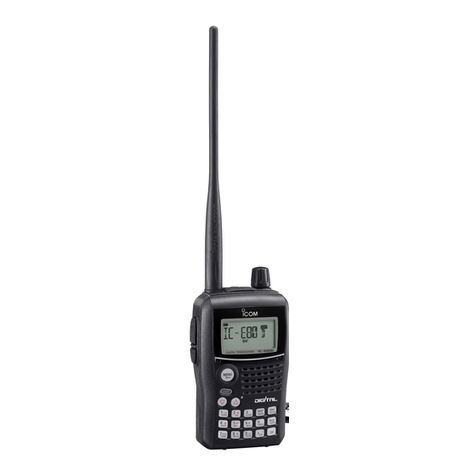
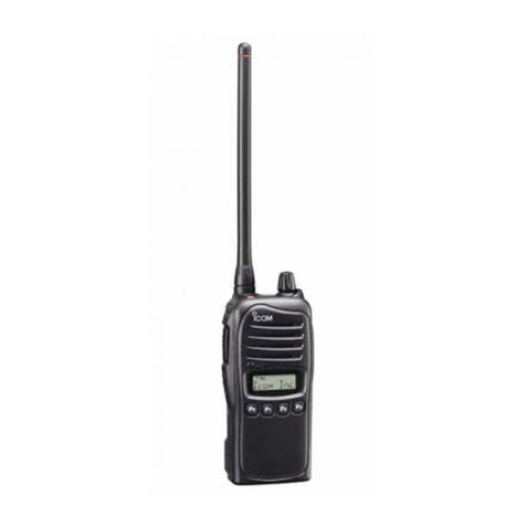
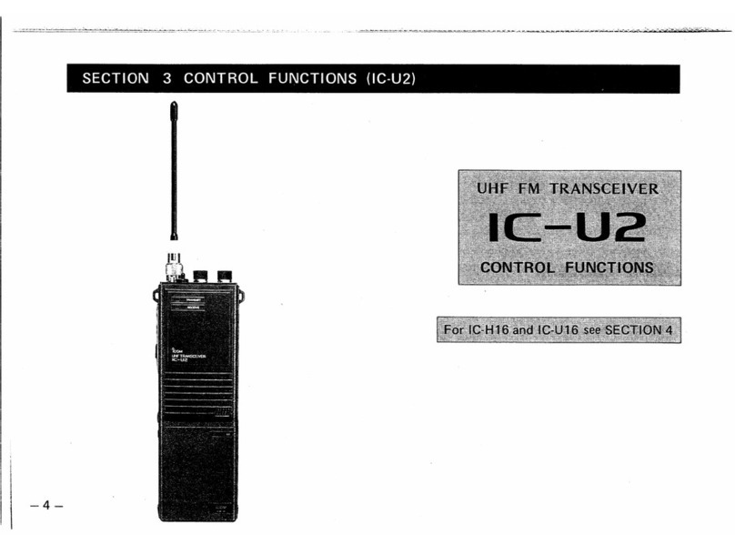
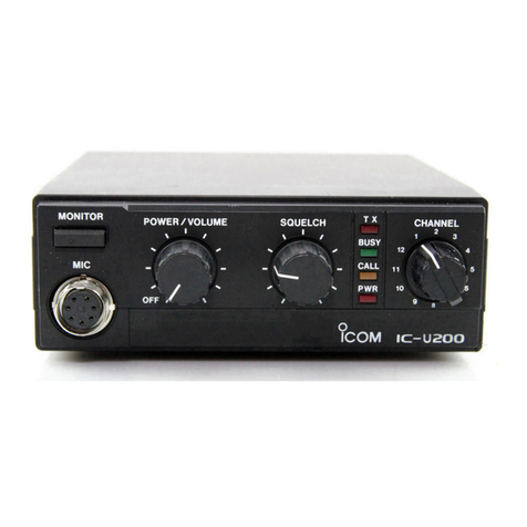
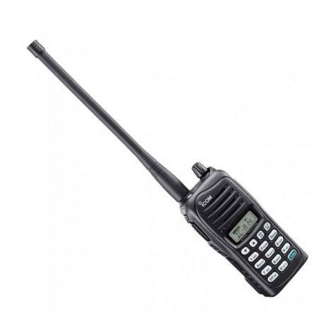
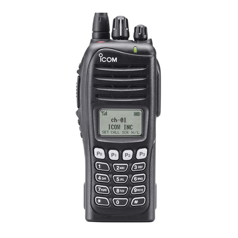
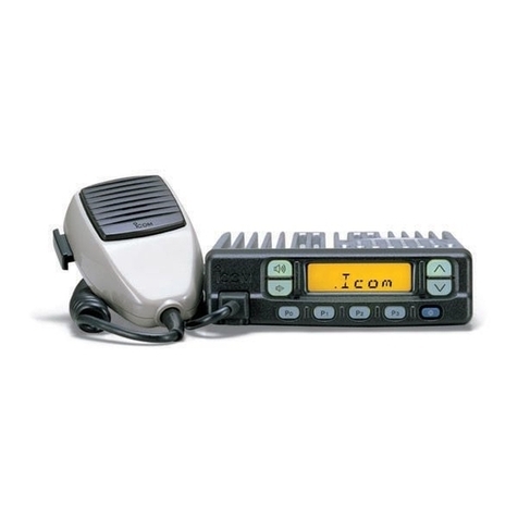
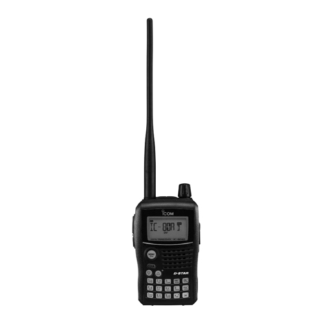
Icom IC-M422 User manual

3%26)#%
-!.5!,
6(&-!2).%42!.3#%)6%2
iC-m422

INTRODUCTION
REPAIR NOTES
This service manual describes the latest service information
for the IC-M422 VHF MARINE TRANSCEIVER at the time
of publication.
DANGER
NEVER connect the transceiver to an AC outlet or to a DC
power supply that uses more than 16 V. Such a connection
could cause a fire or electric hazard.
DO NOT reverse the polarities of the power supply when
connecting the transceiver.
DO NOT apply an RF signal of more than 20 dBm (100 mW)
to the antenna connector. This could damage the trans-
ceiver's front end.
ORDERING PARTS
Be sure to include the following four points when ordering
replacement parts:
1. 10-digit order numbers
2. Component part number and name
3. Equipment model name and unit name
4. Quantity required
<SAMPLE ORDER>
5030002790 LCD A0286 IC-M422 Main unit 5 pieces
8810009510 Screw BO 2x4 NIxZU (BT) IC-M422 Chassis 10 pieces
Addresses are provided on the inside back cover for your
convenience.
1. Make sure the problem is internal before dis-assembling
the transceiver.
2. DO NOT open the transceiver until the transceiver is
disconnected from its power source.
3. DO NOT force any of the variable components. Turn
them slowly and smoothly.
4. DO NOT short any circuits or electronic parts. An
insulated turning tool MUST be used for all adjustments.
5. DO NOT keep power ON for a long time when the
transceiver is defective.
6. DO NOT transmit power into a signal generator or a
sweep generator.
7. ALWAYS connect a 30 dB to 40 dB attenuator between
the transceiver and a deviation meter or spectrum
analyzer when using such test equipment.
8. READ the instructions of test equipment thoroughly
before connecting equipment to the transceiver.
To upgrade quality, all electrical or mechanical parts and internal
circuits are subject to change without notice or obligation.
MODEL COLORS SYMBOL
IC-M422 BLACK [BLK]
SUPER WHITE [SW]
Icom, Icom Inc. and logo are registered trademarks of Icom Incorporated (Japan) in the United States, the United
Kingdom, Germany, France, Spain, Russia and/or other countries.

SECTION 1 SPECIFICATIONS
SECTION 2 INSIDE VIEWS
SECTION 3 DISASSEMBLY INSTRUCTIONS
SECTION 4 CIRCUIT DESCRIPTION
4-1 RECEIVER CIRCUITS . . . . . . . . . . . . . . . . . . . . . . . . . . . . . . . . . . . . . . . . . . . . . . . . 4-1
4-2 TRANSMITTER CIRCUITS . . . . . . . . . . . . . . . . . . . . . . . . . . . . . . . . . . . . . . . . . . . . 4-2
4-3 PLL CIRCUITS . . . . . . . . . . . . . . . . . . . . . . . . . . . . . . . . . . . . . . . . . . . . . . . . . . . . . . 4-3
4-4 DSC CIRCUITS . . . . . . . . . . . . . . . . . . . . . . . . . . . . . . . . . . . . . . . . . . . . . . . . . . . . . 4-3
4-5 PUBLIC ADDRESS (PA) CIRCUIT . . . . . . . . . . . . . . . . . . . . . . . . . . . . . . . . . . . . . . 4-3
4-6 POWER SUPPLY CIRCUITS . . . . . . . . . . . . . . . . . . . . . . . . . . . . . . . . . . . . . . . . . . . 4-4
4-7 CPU PORT ALLOCATIONS . . . . . . . . . . . . . . . . . . . . . . . . . . . . . . . . . . . . . . . . . . . . 4-4
SECTION 5 ADJUSTMENT PROCEDURES
5-1 PREPARATION. . . . . . . . . . . . . . . . . . . . . . . . . . . . . . . . . . . . . . . . . . . . . . . . . . . . . . 5-1
5-2 FREQUENCY ADJUSTMENT . . . . . . . . . . . . . . . . . . . . . . . . . . . . . . . . . . . . . . . . . . 5-2
5-3 TRANSMIT ADJUSTMENT . . . . . . . . . . . . . . . . . . . . . . . . . . . . . . . . . . . . . . . . . . . . 5-3
5-4 RECEIVE ADJUSTMENT . . . . . . . . . . . . . . . . . . . . . . . . . . . . . . . . . . . . . . . . . . . . . 5-4
SECTION 6 PARTS LIST
6-1 IC-M422 . . . . . . . . . . . . . . . . . . . . . . . . . . . . . . . . . . . . . . . . . . . . . . . . . . . . . . . . . . . 6-1
6-2 HM-150B/SW . . . . . . . . . . . . . . . . . . . . . . . . . . . . . . . . . . . . . . . . . . . . . . . . . . . . . . . 6-5
SECTION 7 MECHANICAL PARTS AND DISASSEMBLY
SECTION 8 SEMICONDUCTOR INFORMATION
SECTION 9 BOARD LAYOUTS
9-1 LOGIC BOARD . . . . . . . . . . . . . . . . . . . . . . . . . . . . . . . . . . . . . . . . . . . . . . . . . . . . . 9-1
9-2 HM-150B/SW . . . . . . . . . . . . . . . . . . . . . . . . . . . . . . . . . . . . . . . . . . . . . . . . . . . . . . . 9-1
9-3 VR BOARD. . . . . . . . . . . . . . . . . . . . . . . . . . . . . . . . . . . . . . . . . . . . . . . . . . . . . . . . . 9-3
9-4 SQL BOARD . . . . . . . . . . . . . . . . . . . . . . . . . . . . . . . . . . . . . . . . . . . . . . . . . . . . . . . 9-3
9-5 MAIN UNIT . . . . . . . . . . . . . . . . . . . . . . . . . . . . . . . . . . . . . . . . . . . . . . . . . . . . . . . . . 9-3
SECTION 10 BLOCK DIAGRAM
SECTION 11 VOLTAGE DIAGRAM
11-1 MAIN UNIT . . . . . . . . . . . . . . . . . . . . . . . . . . . . . . . . . . . . . . . . . . . . . . . . . . . . . . . . 11-1
11-2 LOGIC BOARD . . . . . . . . . . . . . . . . . . . . . . . . . . . . . . . . . . . . . . . . . . . . . . . . . . . . . 11-3
SECTION 12 HM-150B/SW
12-1 MECHANICAL PARTS AND DISASSEMBLY . . . . . . . . . . . . . . . . . . . . . . . . . . . . . . 12-1
12-2 VOLTAGE DIAGRAM . . . . . . . . . . . . . . . . . . . . . . . . . . . . . . . . . . . . . . . . . . . . . . . . . 12-1
TABLE OF CONTENTS

1 - 1
SECTION 1 SPECIFICATIONS
MGENERAL
• Frequency coverage : TX
RX
156.025–157.425 MHz
156.050–163.275 MHz
• Type of emission : 16K0G3E, 16K0G2B (DSC)
• Antenna impedance : 50 Ω(Nominal)
• Operating temperature range : –4˚F to +140˚F
• Power supply requirement : 13.8 V DC ±15% (negative ground)
• Current drain (At 13.8 V DC ; approx.) : Receiving
Transmitting
1.5 A (at max. audio)
5.5 A (at 25 W)
• Dimensions (Projections not included) : 6 15/32 (W)×3 1⁄16 (H)×5 15⁄32 (D) in.
• Weight (Approx.) : 2 Ib 5 3⁄4 oz.
MTRANSMITTER
• Output power (At 13.8 V DC) : 25 W (High)/1 W (Low)
• Modulation : Variable reactance frequency modulation
• Maximum frequency deviation : ±5.0 kHz
• Frequency error : Less than ±10 ppm
• Spurious emissions : Less than 70 dBc
• Adjacent channel power : More than 70 dB
• Audio harmonic distortion : Less than 10% (at 60% deviation)
• Residual modulation : More than 40 dB
• Audio frequency response : +1 dB to –3 dB of 6 dB oct. from 300 Hz to 2500 Hz
• Microphone impedance : 2 kΩ
MRECEIVER
• Receive system : Double conversion superheterodyne system
• Intermediate frequencies : 1st IF: 21.7 MHz, 2nd IF: 450 kHz
• Sensitivity : –13 dBµ typical at 12 dB SINAD
• Squelch sensitivity (At threshold) : Less than –13 dBµ
• Adjacent channel selectivity : More than 70 dB
• Spurious response : More than 70 dB
• Intermodulation rejection ratio : More than 70 dB
• Hum and Noise : More than 40 dB
• Audio frequency response : +1 dB to –3 dB of 6 dB oct. from 300 Hz to 3000 Hz
• Audio output power : 4.5 W typical at 10% distortion with a 4 Ω load
• Output impedance (Audio) : 4 Ω
Specifications are measured in accordance with TIA/EIA 603
All stated specifications are subject to change without notice or obligation.

1 - 2
• CHANNEL LISTS
r
e
bm
u
n
l
en
n
a
h
C
A
SU NAC
t
imsnar
T
e
vieceR
1
00
5
0
.
6
5
1 0
5
6
.
0
6
1
A10 0
5
0.651 050.651
20 001.651 007
.
061
30 051.651 057
.
061
A3
00
5
1
.
6
5
1 0
5
1.6
5
1
002.651 008.061
A40 00
2
.65
1002.651
052.651 0
58.
0
61
A50 A
5
00
5
2
.
6
5
1 0
5
2
.65
1
60 60 003.651 003.651
0
5
3
.
6
5
1 0
5
9
.
0
6
1
A
7
0 A
7
0053
.
6
5
1 0
5
3
.
6
5
1
8
080 0
0
4.651 004.651
90 90 054.651 054
.
651
01 0
10
0
5
.
6
5
1 0
0
5.6
5
1
1
111 0
5
5
.
6
5
1 0
5
5
.
6
5
1
21 21 00
6
.65
1006.651
31
2
*
31
1
*
056.
6
51 0
56.
6
5
1
41 41 0
0
7
.
6
5
1 0
0
7
.
6
5
1
51
2*
51
1*
0
5
7
.
6
5
105
7
.65
1
61 61 008.
6
51 008.651
71
1*
71
1*
058
.
6
5
1 0
5
8
.
6
5
1
009.6
5
1 005.161
A8
1A
81 0
0
9
.
651 009.6
5
1
)zHM(
yc
n
e
uq
e
r
F
T
N
I
1
0
20
30
40
50
60
7
0
80
90
0
1
1
1
2
1
3
1
4
1
5
1
1
*
61
7
1
8
1
r
ebmu
n
l
enn
ah
C)z
HM(
y
c
neu
qerF
A
S
UNA
C
t
im
s
n
ar
T
e
v
ie
c
e
R
A
91 A9
105
9
.
65
105
9
.
6
5
1
02 0
2
1
*
0
0
0
.7
51 0
0
6
.
1
61
12 05
0
.
7
5
105
6
.
1
6
1
A
1
2 A
1
2 0
5
0
.7
51 0
50
.
7
51
001.751 0
0
7
.
16
1
A22 A22 001
.
751 0
01
.
7
5
1
3
20
5
1
.
7
5
10
5
7.161
A32 051.751 051.751
4
242 0
02.
7
5
1 0
0
8
.
1
6
1
5
252 0
52.
7
51 0
5
8
.
1
6
1
6
262 003.751 0
09.
1
61
7
272 0
5
3
.
7
5
105
9.
16
1
82 82 0
0
4
.
7
5
1 0
0
0.2
6
1
0
6520
.
651 5
2
6.0
6
1
570
.
651 5
7
6.0
6
1
A
1
6 A
1
6 5
7
0.6
5
1 570.651
521.651 527.0
6
1
A
2
6 5
2
1
.
6
5
1 5
2
1
.
6
5
1
57
1
.65
1577
.
061
A
3
6 5
7
1
.65
1571
.
651
46 5
2
2
.
6
5
1 5
2
8
.
0
6
1
TN
I
0
2
1
2
22
3
2
4
2
5
2
6
2
7
2
8
2
0
6
16
26
36
4
6
A02 00
0
.
7
5
10
0
0
.
75
1
r
e
b
m
u
n
l
e
nn
a
hC
A6
6
)zH
M
(
yc
n
eu
qe
r
F
A6
6
1
*
A
S
UN
AC
ti
m
sn
a
r
T
e
v
i
e
c
eR
A
46 A4
65
2
2.6
5
15
2
2.6
5
1
A
5
6A5
65
72
.
6
51 5
72
.
6
51
5
2
3.6
5
15
2
9.0
6
1
7
6
2*
76 5
73.6
5
1 5
73.6
5
1
8
68
65
24.6
5
15
24.6
5
1
96 9
65
74.6
5
15
74.6
5
1
07
3*
0
7
3
*
5
25.6
5
15
25.6
5
1
17 1
75
75.6
5
1 5
75.6
5
1
2
72
75
26.
6
5
15
26.
6
5
1
37 3
757
6
.651 57
6
.651
47 47 5
27
.
6
51 5
27
.
6
51
77
1*
7
7
1*
5
78
.
6
51 5
78
.
6
51
5
2
9.6
5
1 5
2
5.1
6
1
A
8
7 A
8
75
2
9.
6
51 5
2
9.
6
51
5
79
.
651 5
75
.
1
6
1
A
97 A
97 5
79.651 5
79.6
5
1
520.751 5
26.1
6
1
A
0
8A08 520.751 5
20.751
570.751 576.161
A
1
8A18 5
7
0
.
7
5
1 5
7
0
.
7
5
1
5
2
1
.
7
5
1 5
2
7
.
1
6
1
A28 A
2
85
2
1
.
7
5
1 5
2
1
.
7
5
1
T
N
I
A
5
6
6
6
7
6
8
6
9
6
07
3*
1
7
2
7
37
4
7
7
7
8
7
9
7
08
18
2
8
5
23
.
6
51 5
23
.
6
51
A
6
6
r
eb
m
u
n
l
enn
a
h
C
A4
8
)z
H
M
(
y
c
neuqe
rF
A
S
UN
A
C
t
im
s
n
a
r
T
e
v
i
ec
e
R
A3
8A3
85
7
1
.
75
157
1
.7
5
1
4
84
85
2
2
.
7
5
15
2
8
.
1
6
1
5
85
85
7
2
.
7
5
15
7
8
.
1
6
1
A5
857
2
.
75
157
2
.
7
5
1
68 6
852
3
.
75
152
9
.
1
6
1
A
6
852
3
.
7
5
15
2
3
.
7
5
1
78 7
857
3
.
7
5
15
7
9
.
1
6
1
A
7
857
3
.
7
5
15
7
3
.7
5
1
8
88
852
4
.
7
5
15
2
0
.2
6
1
A8
85
2
4
.
75
152
4
.7
5
1
TN
I
48
58
6
8
7
8
8
8
52
2
.
75
152
2
.
7
5
1
l
e
nn
a
hc
X
W
4
)zH
M
(
y
c
n
e
uqerF
ti
m
s
n
a
r
Te
v
ie
ceR
1 y
l
n
o
X
R0
5
5
.
26
1
2 y
l
n
o
X
R00
4
.
2
6
1
3 y
l
no
X
R574.
2
61
5 y
l
no
X
R05
4
.
2
6
1
6 y
l
no
X
R00
5
.
2
6
1
7 y
l
n
o
X
R 52
5
.
26
1
8 y
l
no
X
R0
5
6
.
16
1
9 y
l
no
X
R5
7
7
.
1
6
1
0
1y
l
n
o
X
R 57
2
.
36
1
y
l
no
X
R52
4
.
2
6
1
1
*
.
yl
nore
w
o
p
wo
L
3*
ylno
no
i
t
a
repoCSD
059
.
6
5
1 0
5
5
.16
1
9
1
b12 y
l
n
oxR 0
5
6
.
16
1
b
5
2 yln
o
xR 058
.
161
5
72
.
6
51 5
78
.
0
615
6
b
82 yl
n
oxR 000.261
38 5
7
1
.
7
5
1 5
7
7
.
1
6
1
3
8
b
3
8y
ln
o
x
R57
7
.
1
6
1
2
*
.
r
e
w
op
hgi
h
yratne
m
o
M
:ET
O
N3
8
d
na
2
8
,1
8
,
4
6
,
16,32
,
12
,3
,s
le
nn
ahc
xe
lpm
i
ST
ON
NA
C
.
s
r
e
t
a
w
.
A
.
S
.
Un
i
c
i
lb
up
l
a
re
negeht
yb
des
u
y
l
lu
f
w
a
l
e
b

2 - 1
SECTION 2 INSIDE VIEWS
• FRONT UNIT
• MAIN UNIT

3 - 1
SECTION 3 DISASSEMBLY INSTRUCTIONS
•REMOVING THE CASE
1Unscrew 4 screws, A.
Note: When replacing the screws, 0.6–0.8 (N.m)
of torque MUST be applied to ensure water resistance.
2Slide the case in the direction of the arrow to separate
the front pannel.
• REMOVING THE MAIN UNIT
1Disconnect W2 from the J2 and J3.
2Disconnect W4 and W5 from the J4 and J5.
3Unsolder the antenna connector, C(2 points).
4Unsolder bottom side D (6 points), as shown below.
5Unscrew 2 screws, E, and 6 screws, F, and 2 clips G
to remove the MAIN unit from the chassis.
3Unscrew 4 screws, B.
Note: When replacing the screws, 0.6–0.8 (N.m)
of torque MUST be applied to ensure water resistance.
4Slide the case in the direction of the arrow to remove the
case.

SECTION 4CIRCUIT DESCRIPTION
4-1 RECEIVER CIRCUITS
4-1-1 ANTENNA SWITCHING CIRCUIT
The antenna switching circuit toggles the receive line and
the transmit line. This circuit does not allow transmit signals
to enter the receiver circuits.
The received signals from the antenna connector (CHASSIS
UNIT; J1) are passed through a two-stage low-pass filter
(LPF; L21, L22, C127–C130, C132) and then applied to the λ/4
type antenna switching circuit (D14, D21).
While receiving, no voltage is applied to D14 and D21. Thus,
the receive line and the ground are disconnected and L31
and C142 function as an LPF which leads received signals
to the RF circuits. The received signals are applied to the RF
circuits via the attenuator (D22).
4-1-2 RF CIRCUITS
The RF circuits amplify received signals within the range of
frequency coverage and filters out-of-band signals.
The received signals from the antenna switch are passed
through a tunable bandpass filter (BPF; D25, L35, C149,
C151, C152, C154) to suppress unwanted signals. The fil-
tered signals are amplified at the RF amplifier (Q21). The
amplified signals are passed through another three-stage
tunable BPF (D26–D28, L36, L38, L39, C161, C162, C164,
C173–C178) to suppress unwanted signals again.
The filtered signals are then applied to the 1st IF circuits.
4-1-3 1st IF CIRCUITS
The 1st IF circuits contain the 1st mixer, IF amplifier and
the 1st IF filter circuits, and the 1st IF mixer converts the re-
ceived signals into a fixed frequency of the 1st intermediate
frequency (IF) signal. The converted 1st IF signal is filtered
at the 1st IF filters, then amplified at the 1st IF amplifier.
The signals from the three-stage tunable BPF are converted
into the 21.7 MHz 1st IF signal at the 1st mixer (Q22) by be-
ing mixed with the 1st LO signal generated at the VCO (Q4,
Q5, D3, D4).
The converted 1st IF signal from the 1st mixer is passed
through the monolithic filters (FI1, FI2) to suppress unwant-
ed signals, and then amplified at the 1st IF amplifier (Q23).
The amplified 1st IF signal is applied to the FM IF IC (IC2, pin 16).
4-1-4 2nd IF AND DEMODULATOR CIRCUITS
The 1st IF signal is converted into the 2nd IF signal and de-
modulated at the detector section in the FM IF IC. The FM IF
IC contains 2nd mixer, limiter amplifier, quadrature detector,
etc. in its package.
The 1st IF signal from the 1st IF amplifier (Q23) is applied to
the mixer section in the FM IF IC (IC2, pin 16). The applied
1st IF signal is mixed with the 21.25 MHz 2nd LO signal from
the PLL IC (IC1, pin 17) to be converted into the 450 kHz 2nd
IF signal.
The 2nd IF signal from the mixer section is output from pin 3
and passed through the ceramic filter (FI3) to suppress the
heterodyne noise. The filtered signal is applied to the FM IF
IC (IC2, pin 5) again, and amplified at the limiter amplifier
section and demodulated by the quadrature detector.
The demodulated AF signals are output from pin 9, and ap-
plied to the AF cricuits.
4-1-5 AF CIRCUITS
The demodulated AF signals from the FM IF IC are amplified
and filtered in AF circuits.
The AF signals from FM IF IC (IC3, pin 9) are passed
through the BPF (Q31, Q32) and AF mute switch (IC4, pins 8, 9),
and then applied to the volume control pot (VR BOARD; R1)
to be adjusted its level. The level adjusted AF signals are
applied to the AF power amplifier (IC9, pin1) to obtain 4.5 W
(typ.) of AF output power.
The power amplified AF signals are output from pin 4, and
applied to the internal speaker (FRONT UNIT; SP1) via J4 or
connected external speaker/hailer.
4 - 1
Mixer
Quadrature
detector
1st IF signal from the IF amplifier (Q23)
16
Noise
detector
R5V
X2
1110
IC2
TA31136FN
Filter
amp.
Limiter
amp.
demodulated signals
to the AF circuits
• 2ND IF AND DEMODULATOR CIRCUITS
9
R214
“SQL” signal to the CPU (LOGIC BOARD; IC1, pin 5)
14
IC11
Squelch amp.
–
+
21.25 MHz
2
17
X1
21.25 MHz
8735
FI3 PLL IC
(IC1)

4 - 2
4-1-6 SQUELCH CIRCUITS
Noise squelch circuit mutes AF output signals when no RF
signals are received. By detecting noise components in the
demodulated AF signals, the squelch circuit switches the AF
mute switch ON and OFF.
A portion of the demodulated AF signals from the FM IF IC
(IC2, pin 9) are passed through the squelch adjustment pot
(R214) to be adjusted its level. The level adjusted AF signals
are passed through the active filter (IC2, pins 7, 8; R211–R213,
C211, C212, C217). The filtered signals are then applied to
the noise amplifier section in the IC2 to amplify the noise
components only.
The amplified noise components are converted into the
pulse-type signal at the noise detector section, and output
from pin 14 as the “SQL” signal. The “SQL” signal is applied
to the squelch amplifier (IC11, pin 1) to be amplified its level,
then output from pin 4. The amplified “SQL” signal is applied
to the CPU (LOGIC BOARD; IC1, pin 5). Then the CPU out-
puts “RMUTEM” signal from pin 64 according to the “SQL”
signal level to toggle the AF mute circuit (IC4) ON/OFF.
4-2 TRANSMITTER CIRCUITS
4-2-1 MICROPHONE AMPLIFIER CIRCUIT
The microphone amplifier circuit amplifies the audio signals
from microphone (MIC signals) within +6 dB/oct pre-emphasis
characteristic.
The MIC signals from the microphone (HM-150B/SW; MC1)
are passed through the microphone mute switch (IC5, pins
10, 11) and amplified at the microphone amplifier (IC7, pin
6) to obtain +6 dB/oct pre-emphasis characteristics. The am-
plified MIC signals are limited its level at the IDC amplifier
(IC7, pin 5), and filtered out 3 kHz and higher audio signals
at the LPF (IC8, pins 5, 7).
The filtered MIC signals are passed through the deviation
adjustment pot (R327) to be adjusted its level. Then the level
adjusted MIC signals are applied to the modulation circuit.
4-2-2 MODULATION CIRCUIT
The modulation circuit modulates the VCO oscillating signal
with the audio signals from the microphone.
The level adjusted MIC signals are applied to the modulation
circuit (D2) to modulate the VCO oscillating signal by chang-
ing the reactance of D2 at the VCO (Q4, Q5, D3, D4).
The modulated VCO output signals are amplified at the buf-
fer amplifiers (Q6, Q7), then applied to the transmit ampli-
fiers via the TX/RX switch (D7).
4-2-3 TRANSMIT AMPLIFIERS
The VCO output signals are amplified to transmit output
power level by the transmit amplifiers .
The buffer-amplified VCO output signals from the TX/RX
switch (D7) are applied to the pre-drive (Q10), YGR (Q12),
and power (IC3) amplifiers to be amplified to the transmit out-
put power level. The power amplified transmit signal is passed
through the power detector (D12, D13), antenna switch
(D14) and a two-stage LPF (L21, L22, C127–C130, C132),
and then applied to the antenna connector (CHASSIS UNIT; J1).
4-2-4 APC CIRCUIT
The APC (Automatic Power Control) circuit stabilizes trans-
mit output power and controls transmit output power High (25 W)
or Low (1 W).
The power detector circuits (D12, D13) detect the transmit
output signal level and converts it into DC voltage. The de-
tected voltage is applied to the APC amplifier (IC12, pin 3). The
voltage of the “T5V” line is applied to another input (pin 1)
via the transmit output power adjustment pot (R112) as the
reference voltage.
The output voltage from the APC amplifier controls the bias
of the power amplifier (IC3) to control the output power by
comparing the detected voltage and the reference voltage.
Thus the APC circuit maintains a constant transmit output
power.
Power
amp.
APC
amp.
YGR
amp.
+
–
HV
TXDET
• APC CIRCUIT
to the anntena
T5V
R112
T5V
TMUTE
H/L
from TX/RX switch (D7)
Q12
Pre-drive
amp.
Q10
IC12
Q17
IC3
LPF ANT
SW
D12
Power detector
D13
D14

4 - 3
4-3 PLL CIRCUITS
4-3-1 VCO CIRCUIT
The VCO circuit (Q4, Q5, D3, D4) directly generates both of the
1st LO frequency for receiving (134.35–141.575 MHz) and the
transmit frequency (156.025–157.425 MHz).
While receiving, the VCO output signal (1st LO signal) is am-
plified at the buffer amplifiers (Q6, Q7) and passed through
the TX/RX switch (D8), then applied to the 1st mixer (Q22).
While transmitting, the VCO output signal (transmit signal)
is amplified at the buffer amplifiers (Q6, Q7) and passed
through the TX/RX switch (D7), then applied to the pre-driver
(Q10).
A portion of the VCO output signal from the buffer amplifier
(Q6) is fed back to the PLL IC (IC1, pin 2) as the comparison
signal via the buffer amplifier (Q3) and the LPF (L2, C34,
C35).
4-3-2 PLL CIRCUIT
The PLL circuit provides stable oscillation of the transmit
frequency and receive 1st LO frequency. The PLL circuit
compares the phase of the divided VCO frequency with the
reference frequency. The PLL output frequency is controlled
by the divided ratio of the programmable divider.
The buffer amplified signals are applied to the PLL IC (IC1,
pin 2) via the LPF (L2, C34, C35). The applied signals are
divided at the prescaler and programmable counter section
according to the “PDATA” from the CPU (LOGIC BOARD; IC1
pin 8). The divided signal is phase-compared with the reference
frequency at the phase detector.
The phase difference is output from pin 8 as a pulse type
signal after being passed through the charge pump section.
The output signal is passed through the loop filter (R7–R9,
R41, C4, C5, C43, C44) to be converted into the DC voltage,
and is then applied to the VCO circuits as the lock voltage.
If the oscillated signal drifts, its phase changes from that of
the reference frequency, causing a lock voltage change to
compensate for the drift in the oscillated frequency.
4-4 DSC CIRCUITS
• DECODING
A portion of the demodulated AF signals from the FM IF IC
(IC2, pin 9) are passed through the LPF (Q38) to filter DSC
signal. The filtered DSC signal is applied to the DSC de-
coder (IC15, pin 2). The decoded DSC signal is output from
pin7, and then applied to the CPU (LOGIC BOARD; IC1, pin
14). Then the CPU controls the transceiver according to the
DSC content.
• ENCODING
The DSC signals (FSK) are generated by the CPU (LOGIC
BOARD; IC1) and output from pins 141. The DSC signals
are applied to the buffer amplifier (LOGIC BOARD; IC5,
pin 3). The buffer amplified DSC signals are output from
pin 1, and passed through the LPF (IC8, pins 5, 7), and
applied to the modulation circuit (D2) via the deviation
adjustment pot (R327) to modulate the VCO oscillating
signal.
4-5 PUBLIC ADDRESS (PA) CIRCUIT
The Public Address (PA) circuit power amplifies the audio
signals from the microphone. The power amplified MIC sig-
nals are output to the connected external speaker or hailer.
The MIC signals from the microphone (HM-150B/SW or
optional HM-157) are passed through the AF mute circuit
(IC5, pins 10, 11), and applied to the microphone amplifier
(IC8, pin 2). The amplified MIC signals are output from pin 1,
and applied to the electric volume controller (IC13, pin 1) via
the AF mute circuit (IC5, pins 8, 9). The volume controlled
MIC signals are then passed through the AF mute circuit
(Q65), and applied to the AF power amplifier (IC14, pin 1) to
be amplified to obtain 5 W (min.) of AF output power.
The power amplified AF signals are output from pin 4, and
applied to the connected external speaker or hailer.
DATA interface
Prescaler
Phase
detector
Loop
filter
Reference
counter
Programmable
counter
Charge
pump
Buffer
Q6
Buffer
Q7
Buffer
Q3 to the TX/RX switch (D7, D8)
Q4, Q5, D3, D4
VCO
LPF
to the FM IF IC (IC2, pin 2)
3
8
72
17
15
16
PSTB
UNLK
• PLL CIRCUITS
PCK
PDATA
X1
4
5
S5V
IC1
µPD3140GS

4 - 4
4-7 CPU PORT ALLOCATIONS
Pin
NO. Port name Description
2 KEYM
Input port for keys on HM-150B/SW.
Approx. 2.02 V: [Y] key is pushed.
Approx. 3.00 V: [Z] key is pushed.
Approx. 3.84 V: [H/L] key is pushed.
3 TXDET Input port for transmit detected voltage.
4 LBAT Input port for low battery detecting.
5 SQL Input port for "NOISE" signal from the squelch
amplifier (IC11, pin 4).
6 SQLV Input port for squelch adjustment pot (SQL
BOARD; R1).
7 WXDEC Input port for weather alert signal from the
LPF (Q38).
8 PDATA Outputs data signal to the PLL IC (IC1, pin 5).
9 PCK Outputs clock signal to the PLL IC (IC1, pin 4).
10 PSTB Outputs strobe signal to the PLL IC (IC1, pin3).
12 EVDATA Outputs volume control signal to the volume
ccontroller (IC13, pin 5) for PA circuit.
13 EVCK Outputs clock signal to the volume ccontroller
(IC13, pin 4) for PA circuit.
14 DSDEC Input port for the DSC decode signal from the
DSC decoder (IC15, pin 7).
28,
29
CONT1,
CONT0
Output LCD contrast adjust signal to the CPU
(IC1, pin 134).
32 COMTXD Outputs serial data signal to the connected
HM-157 (Optional product).
33 COMRXD Input port for the serial data signal from the
connected HM-157 (Optional product).
34 ECK Outputs clock signal to the EEPROM (LOGIC
BOARD; IC4, pin 6).
35 EDATA I/O port for the EEPROM (LOGIC BOARD;
IC4, pin 5) control data.
37 NMTXD Outputs NMEA command signal.
Pin
NO. Port name Description
38 NMRXD Input port for the NMEA signal.
48 PWR Input port for power switch (VR BOARD; R1).
Low: When [VOL] is pushed.
49 PAMUTE
Outputs control signal to the AF (Public Ad-
dress) mute circuit (Q65).
High: During mute.
50 PWRON
Outputs power control signal to the power
control circuit (Q61, Q62).
High: While the transceiver is switched ON.
51 TMUTE
Outputs transmit mute signal to the APC circuit
(IC12, pin 3).
High: During mute.
53 RCV
Outputs control signal to the R5 control circuit
(Q53, Q54).
High: While receiving.
54 H/L
Outputs TX power control signal to the TX
power control circuit (Q17, D11).
High: 25 W
Low: 1 W
55 ATT
Outputs attenuator control signal to the
attenuator (D22).
High: Attenuator ON.
57 PTT Input port for the [PTT] switch (HM-150B/SW; S1).
Low: [PTT] key is pushed.
60 UNLK
Input port for the "UNLK" signal from the PLL
IC (IC1, pin7).
High: PLL circuit is unlocked.
61 DTRS
Input port for the [DISTRESS] key (LOGIC
BOARD; S9).
Low: [DISTRESS] key is pushed.
62 RMUTEP
Outputs AF (Public Address) mute signal to
the AF mute circuit (IC4, pin12).
Low: During mute.
63 RMUTES
Outputs AF mute signal to the AF mute circuit
(IC4, pin 5) for the connected HM-157 (Op-
tional product).
Low: During mute.
64 RMUTEM
Outputs AF (internal speaker) mute signal to the
AF mute circuit (IC4, pin 6).
Low: During mute.
65 MMUTEP
Outputs microphone (Public Address) mute
signal to the AF mute circuit (IC5, pin 6).
Low: During mute.
66 MMUTES
Outputs microphone mute signal to the AF
mute circuit (IC5, pin 5) for the connected
HM-157 (Optional product).
Low: During mute.
67 MMUTEM
Outputs microphone (HM-150B/SW) mute sig-
nal to the AF mute circuit (IC5, pin 13).
Low: During mute.
68 PTTS
Outputs AF/MIC control signal to the AF mute
circuit (IC6, pin 5).
High: PTT switch (HM-157) is pushed
69 PTTM Outputs AF/MIC control signal to the AF mute
circuit (IC5, pin 12).
70 LO/DX
Input port for the [LO/DX] key (LOGIC
BOARD; S8).
Low: [LO/DX] key is pushed.
4-6 POWER SUPPLY CIRCUITS
Line Description
HV The voltage from the connected DC power supply.
L5V
Common 5V converted from the HV line at the L5V regulator
(LOGIC BOARD; IC3).
The converted voltage is applied to the CPU (LOGIC
BOARD; IC1)
VCC Same voltage as the HV line whitch is passed through the
power control circuit (Q61, Q62).
S5V Common 5V converted from the VCC line at the +5 regulator
circuit (IC10).
T5 Transmit 5V controlled by the T5 control circuit (Q52, Q57)
using the "SEND" signal from CPU (LOGIC BOARD; IC1, pin 52).
R8
Receive 8 V converted from the VCC line at the R8 regulator
(Q55, Q56).
The converted voltage is applied to the receiver circuits.
R5
Receive 5V controlled by the R5 control circuit (Q53, Q54)
using the "RCV" signal from CPU (LOGIC BOARD; IC1,
pin 53).
The controlled voltage is applied to the receiver circuits.

4 - 5
Pin
NO. Port name Description
71 DSC Input port for the [DSC] key (LOGIC BOARD; S7).
Low: [DSC] key is pushed.
72 PA Input port for the [PA] key (LOGIC BOARD; S6).
Low: [PA] key is pushed.
73 CH/WX
Input port for the [CH/WX] key (LOGIC
BOARD; S5).
Low: [CH/WX] key is pushed.
74 SCAN Input port for the [SCAN] key (LOGIC BOARD; S4).
Low: [SCAN] key is pushed.
75 CH16 Input port for the [16] key (LOGIC BOARD; S3).
Low: [16] key is pushed.
76 DOWN Input port for the [Z] key (LOGIC BOARD; S2).
Low: [Z] key is pushed.
77 UP Input port for the [Y] key (LOGIC BOARD; S1).
Low: [Y] key is pushed.
138 DIM Outputs dimmer control signal to the LCD control
circuit (LOGIC BOARD; Q2, Q3).
139 BEEP Outputs beep signal to the AF amplifier (IC9, pin 1).
141 DS/BPF
• While transmitting:
Outputs DSC encode signal as "DSENC"
to the LPF (IC8, pin 5) via the buffer amplifier
(LOGIC BOARD; IC5, pins 1, 3).
• While receiving:
Outputs tuning signal as "BPFV" to the
tunable BPFs (D25–D28) via buffer amplifier
(LOGIC BOARD; IC5, pins 5, 7).
4-7 PORT ALLOCATIONS (continued)

5 - 1
EQUIPMENT GRADE AND RANGE EQUIPMENT GRADE AND RANGE
DC power supply Output voltage : 13.8 V DC
Current capacity : More than 10 A Audio generator Frequency range : 300–3000 Hz
Measuring range : 1–500 mV
RF power meter
(terminated type)
Measuring range : 1–30 W
Frequency range : 100–300 MHz
Impedance : 50 Ω
SWR : Less than 1.2 : 1
Standard signal
generator (SSG)
Frequency range : 0.1–300 MHz
Output level : 0.1 µV to 32 mV
(–127 to –17 dBm)
Frequency counter
Frequency range : 0.1–300 MHz
Frequency accuracy: ±1 ppm or better
Sensitivity : 100 mV or better
Oscilloscope Frequency range : DC to 20 MHz
Measuring range : 0.01–20 V
FM deviation meter Frequency range : 30–300 MHz
Measuring range : 0 to ±10 kHz AC millivoltmeter Measuring range : 10 mV to 10 V
DC volt meter Input impedance : 50 kΩ/V DC or more
External speaker Input impedance : 4 Ω
Capacity : More than 5 W
Attenuator Power attenuation : 40 or 50 dB
Capacity : More than 30 W
SECTION 5 ADJUSTMENT PROCEDURES
5-1 PREPARATION
MREQUIRED TEST EQUIPMENTS
To the antenna connector
To DC power connector
Standard signal
generator
0.1 µV to 32 mV
(–127 to –17 dBm)
CAUTION:
DO NOT transmit while SSG is connected
to the antenna connector.
DC power supply
13.8 V /10 A
Frequency
counter
FM deviation
meter
Attenuator
40 dB or 50 dB
+
–
Red
Black
RF power meter
1–30 W
To external speaker lead
Distortion meter
AC millivoltmeter
Speaker (4 Ω)
SP+ (Yellow)
SP− (Black)
MCONNECTION

ADJUSTMENT ADJUSTMENT
CONDITION
MEASUREMENT VALUE
ADJUSTMENT
POINT
UNIT OPERATION UNIT ADJUST
LOCK
VOLTAGE
1 • Channel : CH16 (156.800 MHz)
• Receiving
MAIN Connect a digital multi-
meter or oscilloscope
to the check point "CP1".
1.1–2.1 V MAIN Verify
2 • Channel : CH16 (156.800 MHz)
• Output power : Low
•Transmitting
0.9–1.9 V Verify
REFERENCE
FREQUENCY
1 • Channel : CH16 (156.800 MHz)
• Output power : Low
• Connect a power meter to the antenna
connector.
• Transmitting
Rear
Panel
Loosely couple a fre-
quency counter to the
antenna connector.
156.800 MHz
±500 Hz
MAIN C12
CP1
Lock voltage
check point
Reference frequency
adjustment
C12
5-2 FREQUENCY ADJUSTMENT
5 - 2

5 - 3
ADJUSTMENT ADJUSTMENT CONDITION MEASUREMENT VALUE
ADJUSTMENT
POINT
UNIT OPERATION UNIT ADJUST
OUTPUT
POWER
1 • Channel : CH16 (156.800 MHz)
• Output power : High
• Transmitting
Rear
Panel
Connect an RF power
meter to the antenna
connector.
23–23.5 W MAIN R112
FREQUENCY
DEVIATION
1 • Channel : CH16 (156.800 MHz)
• Output power : Low
• Connect an audio generator to the pin 28
of J4 (MAIN UNIT) and set as;
Frequency : 1 kHz
Level : 30 mV
• Set the FM deviation meter as;
HPF : OFF
LPF : 20 kHz
De-emphasis: OFF
Detector : (P−P)/2
• Transmitting
Rear
Panel
Connect an FM
deviation meter to the
antenna con-nector
through an attenuator.
±4.25–4.35 kHz MAIN R327
R112
R327
Output power adjustment
Frequency deviation
adjustment
+
–
+
–
AC millivoltmeter
Audio generator
J4
29
28
5-3 TRANSMIT ADJUSTMENT

5 - 4
ADJUSTMENT ADJUSTMENT CONDITION MEASUREMENT VALUE
ADJUSTMENT
POINT
UNIT OPERATION UNIT ADJUST
SENSITIVITY 1 • Channel : CH16 (156.800 MHz)
• [SQL] : Max. counterclockwise
• Connect a distortion meter with a 4 Ω
load to the external speaker lead.
• Push [PA•RX ] for 1 sec. to turn the
RX speaker mode ON.
• Connect an SSG to the antenna
co nnector and set as ;
Frequency : 156.800 MHz
Level : +10 dBµ
Modulation :1 kHz
Deviation : ±3 kHz
• Receiving
MAIN Connect a DC volt meter
or oscilloscope to the
check
point "CP3".
Maximum
voltage
MAIN L35,L36, L38,
L39
(Repeate two
times or more.)
SQUELCH 1 • Channel : CH16 (156.800 MHz)
• [SQL] : Max. counterclockwise
• Set the SSG as;
Level : −12 dBµ
• Receiving
MAIN Connect a volt meter
or
oscilloscopeto the
check point "CP5".
1.0 V MAIN R214
5-4 RECEIVE ADJUSTMENT
L36
L35
L38
CP3
Sensitivity check point
R214
Squelch adjustment
CP5
Squelch check point
Sensitivity
adjustment
L39

6 - 1
SECTION 6 PARTS LIST
M.=Mounted side (T: Mounted on the Top side, B: Mounted on the Bottom side)
REF ORDER DESCRIPTION M. H/V
NO. NO.
LOCATION
[FRONT UNIT]
MC1 0800007890 MIC HM-150B ACC <FG> [BLK]
0800007900 MIC HM-150SW ACC <FG> [SW]
SP1 2510001240 SP 045P0803 <FG>
W1 7120000470 JMP ERDS2T0
W2 7120000470 JMP ERDS2T0
IC1 1140012751 S.IC M30220MA-137RP B 48.1/48.5
IC2 1110005770 S.IC S-80942CNMC-G9C-T2 B 79.7/48.8
IC3 1180000970 S.IC AN78L05M-(E1) B 55.3/20.8
IC4 1140008650 S.IC HN58X2464TI B 51.9/27.7
IC5 1110002700 S.IC NJM2904M-TE1 B 39.3/7.7
IC6 1170000350 S.IC PC357N6T B 77.2/11.6
IC7 1130007420 S.IC TC7W14FU (TE12L) B 22/44.5
Q1 1520000840 S.TR KTA1664Y-RTF/P B 74/18.8
Q2 1530003900 S.TR KTC4075 BL-RTK/P B 69.7/17.5
Q3 1530003900 S.TR KTC4075 BL-RTK/P B 69.7/21.3
Q4 1590003590 S.TR KRC414 RTK/P B 46.3/28.6
Q5 1530002280 S.TR 2SC4081 T106 S B 11.8/34.8
Q6 1590003580 S.TR KRC404 RTK/P B 15.6/34.6
Q7 1530002280 S.TR 2SC4081 T106 S B 22.7/49.7
Q8 1510000510 S.TR 2SA1576A T106R B 19.6/51
Q9 1560000810 S.FET 2SK1069-4-TL B 26.7/39.6
D1 1750001180 S.DIO KDS122 RTK/P B 47.5/25.8
D2 1750000550 S.DIO 1SS355 TE-17 B 83.7/11.4
D3 1750001180 S.DIO KDS122 RTK/P B 13.4/31.7
D4 1730002360 S.ZEN MA8062-M (TX) B 12.7/29.2
X1 6050011500 S.XTL CR-739 (9.8304 MHz) B 60.8/34
R1 7030003640 S.RES ERJ3GEYJ 473 V (47 kΩ) B 54.2/37.2
R2 7030003640 S.RES ERJ3GEYJ 473 V (47 kΩ) B 54.9/35.9
R3 7030003800 S.RES ERJ3GEYJ 105 V (1 MΩ) B 56.2/38.3
R4 7030003320 S.RES ERJ3GEYJ 101 V (100
Ω) B 57.3/40.3
R5 7030003640 S.RES ERJ3GEYJ 473 V (47 kΩ) B 63.2/40.4
R6 7030003560 S.RES ERJ3GEYJ 103 V (10 kΩ) B 63.2/41.7
R11 7030005631 S.RES ERA3YKD 154V (150 kΩ) B 67.4/47.6
R12 7030005681 S.RES ERA3YKD 473V (47 kΩ) B 67.4/48.9
R13 7030003560 S.RES ERJ3GEYJ 103 V (10 kΩ) B 64.2/33.4
R14 7030003460 S.RES ERJ3GEYJ 152 V (1.5 kΩ) B 74/48.1
R15 7030003570 S.RES ERJ3GEYJ 123 V (12 kΩ) B 71.4/48.1
R16 7030003530 S.RES ERJ3GEYJ 562 V (5.6 kΩ) B 72.7/48.1
R17 7030003560 S.RES ERJ3GEYJ 103 V (10 kΩ) B 59.4/54.7
R18 7030003560 S.RES ERJ3GEYJ 103 V (10 kΩ) B 62/53.9
R19 7030003560 S.RES ERJ3GEYJ 103 V (10 kΩ) B 60.7/53.3
R21 7030003560 S.RES ERJ3GEYJ 103 V (10 kΩ) B 80.9/51.9
R22 7030003640 S.RES ERJ3GEYJ 473 V (47 kΩ) B 76.7/48.1
R23 7030003640 S.RES ERJ3GEYJ 473 V (47 kΩ) B 77/50.9
R25 7030010610 S.RES ERJ1TYJ 470U (47
Ω) B 61.9/19.3
R31 7030003640 S.RES ERJ3GEYJ 473 V (47 kΩ) B 51.9/33.6
R32 7030003560 S.RES ERJ3GEYJ 103 V (10 kΩ) B 51.9/34.9
R35 7030003580 S.RES ERJ3GEYJ 153 V (15 kΩ) B 45.3/25.9
R36 7030003440 S.RES ERJ3GEYJ 102 V (1 kΩ) B 44/25.3
R37 7030003440 S.RES ERJ3GEYJ 102 V (1 kΩ) B 44.5/31.3
R41 7030003500 S.RES ERJ3GEYJ 332 V (3.3 kΩ) B 44.9/11.2
R42 7030003680 S.RES ERJ3GEYJ 104 V (100 kΩ) B 44.2/6.4
R43 7030003800 S.RES ERJ3GEYJ 105 V (1 MΩ) B 45.8/6.4
R45 7030005321 S.RES ERA3YED 103V B 33.2/7.7
S.=Surface mount
REF ORDER DESCRIPTION M. H/V
NO. NO.
LOCATION
[LOGIC BOARD]
REF ORDER DESCRIPTION M. H/V
NO. NO.
LOCATION
[LOGIC BOARD]
R46 7030008121 S.RES ERA3YED 682V B 34.5/7.7
R48 7030003860 S.RES ERJ3GE JPW V B 33.2/10.5
R51 7030003250 S.RES ERJ3GEYJ 270 V (27
Ω) B 71.9/22.7
R52 7030003250 S.RES ERJ3GEYJ 270 V (27
Ω) B 73.2/22.7
R53 7030003250 S.RES ERJ3GEYJ 270 V (27
Ω) B 74.5/22.7
R60 7030003630 S.RES ERJ3GEYJ 393 V (39 kΩ) B 66.8/19.5
R61 7030003640 S.RES ERJ3GEYJ 473 V (47 kΩ) B 66.8/16.9
R62 7030003440 S.RES ERJ3GEYJ 102 V (1 kΩ) B 68.8/24
R63 7030003560 S.RES ERJ3GEYJ 103 V (10 kΩ) B 69.7/19.4
R64 7030003460 S.RES ERJ3GEYJ 152 V (1.5 kΩ) B 67.5/21.6
R71 7030003430 S.RES ERJ3GEYJ 821 V (820
Ω) B 84.9/6
R72 7030003430 S.RES ERJ3GEYJ 821 V (820
Ω) B 12.1/12.2
R73 7030003430 S.RES ERJ3GEYJ 821 V (820
Ω) B 11.4/8.7
R74 7030003380 S.RES ERJ3GEYJ 331 V (330
Ω) B 12.4/50.4
R75 7030003380 S.RES ERJ3GEYJ 331 V (330
Ω) B 12.4/39
R76 7030003380 S.RES ERJ3GEYJ 331 V (330
Ω) B 12.4/43.9
R81 7030003430 S.RES ERJ3GEYJ 821 V (820
Ω) B 87.3/10
R82 7030003520 S.RES ERJ3GEYJ 472 V (4.7 kΩ) B 21.4/39.5
R83 7030003440 S.RES ERJ3GEYJ 102 V (1 kΩ) B 70.9/12
R85 7030003680 S.RES ERJ3GEYJ 104 V (100 kΩ) B 12.7/27.5
R86 7030003210 S.RES ERJ3GEYJ 120 V (12
Ω) B 11.2/31.7
R87 7030003520 S.RES ERJ3GEYJ 472 V (4.7 kΩ) B 13.7/34.8
R88 7030003680 S.RES ERJ3GEYJ 104 V (100 kΩ) B 14.4/36.8
R91 7030003520 S.RES ERJ3GEYJ 472 V (4.7 kΩ) B 19.6/49.1
R92 7030003280 S.RES ERJ3GEYJ 470 V (47
Ω) B 24.8/48.8
R95 7030003440 S.RES ERJ3GEYJ 102 V (1 kΩ) B 26.1/36.8
R96 7030003640 S.RES ERJ3GEYJ 473 V (47 kΩ) B 24.8/36.8
R97 7030003440 S.RES ERJ3GEYJ 102 V (1 kΩ) B 23.1/39.9
R101 7030003320 S.RES ERJ3GEYJ 101 V (100
Ω) B 19.1/14.6
R103 7030003860 S.RES ERJ3GE JPW V B 20.5/14.6
R104 7030003860 S.RES ERJ3GE JPW V B 22.6/16.6
R106 7030003640 S.RES ERJ3GEYJ 473 V (47 kΩ) B 17/16.9
C1 4550006210 S.TAN ECST1CX106R B 56.3/30
C2 4030006900 S.CER C1608 JB 1H 103K-T B 55.6/33.7
C3 4030009650 S.CER C1608 CH 1H 240J-T B 57.5/35.5
C4 4030009650 S.CER C1608 CH 1H 240J-T B 57.5/38.3
C5 4030006860 S.CER C1608 JB 1H 102K-T B 88.9/39.3
C6 4030006850 S.CER C1608 JB 1H 471K-T B 88.9/42.2
C7 4030011600 S.CER C1608 JB 1E 104K-T B 37.3/55.1
C8 4030006860 S.CER C1608 JB 1H 102K-T B 36.6/34.4
C11 4030008920 S.CER C1608 JB 1H 473K-T B 68.7/43.1
C12 4030008920 S.CER C1608 JB 1H 473K-T B 68.4/44.4
C13 4030008920 S.CER C1608 JB 1H 473K-T B 67.7/46.1
C14 4030008920 S.CER C1608 JB 1H 473K-T B 67.4/50.2
C15 4030008920 S.CER C1608 JB 1H 473K-T B 64.1/50.8
C16 4030008920 S.CER C1608 JB 1H 473K-T B 65.4/50.8
C17 4030011600 S.CER C1608 JB 1E 104K-T B 62.8/51.2
C18 4030006900 S.CER C1608 JB 1H 103K-T B 70.6/50.2
C21 4030017480 S.CER C1608 JB 1A 474K-T B 78.3/51.9
C22 4030008890 S.CER C1608 JB 1H 273K-T B 79.6/51.9
C25 4510004630 S.ELE ECEV1CA100SR B 49.6/19.7
C26 4030006900 S.CER C1608 JB 1H 103K-T B 59.4/20.7
C27 4550006210 S.TAN ECST1CX106R B 58/25
C28 4030006900 S.CER C1608 JB 1H 103K-T B 54.4/25
C31 4030011600 S.CER C1608 JB 1E 104K-T B 52.8/32.3
C41 4030011600 S.CER C1608 JB 1E 104K-T B 36.5/11.2
C42 4030007170 S.CER C1608 CH 1H 221J-T B 42.1/11.2
C43 4030007010 S.CER C1608 CH 1H 100D-T B 39.3/11.2
C51 4510004630 S.ELE ECEV1CA100SR B 77.6/23.5
C52 4030006860 S.CER C1608 JB 1H 102K-T B 70.1/24
C54 4030011600 S.CER C1608 JB 1E 104K-T B 66.8/18.2
C81 4030012660 S.CER C1608 JB 1E 683K-T B 85.3/11.1
C82 4030006900 S.CER C1608 JB 1H 103K-T B 72.3/12
C83 4030011600 S.CER C1608 JB 1E 104K-T B 23/36.5
C86 4030011600 S.CER C1608 JB 1E 104K-T B 17.8/33.8
C87 4030006860 S.CER C1608 JB 1H 102K-T B 11.6/37
C88 4030006860 S.CER C1608 JB 1H 102K-T B 83.3/7.8
C89 4030006860 S.CER C1608 JB 1H 102K-T B 82.1/11.2
C90 4030006860 S.CER C1608 JB 1H 102K-T B 71.5/9.9
C91 4030011600 S.CER C1608 JB 1E 104K-T B 22.7/51.6
C95 4030011600 S.CER C1608 JB 1E 104K-T B 19.5/43.5
C101 4030006860 S.CER C1608 JB 1H 102K-T B 17/15.6
C102 4030006860 S.CER C1608 JB 1H 102K-T B 17/13.9
C103 4030006850 S.CER C1608 JB 1H 471K-T B 23.3/14.6
C104 4030006860 S.CER C1608 JB 1H 102K-T B 25.4/13.9
C111 4030006860 S.CER C1608 JB 1H 102K-T B 7.4/15.7
C112 4030006860 S.CER C1608 JB 1H 102K-T B 9/53
C113 4030006860 S.CER C1608 JB 1H 102K-T B 48.6/7.2
C114 4030006850 S.CER C1608 JB 1H 471K-T B 47.2/7.2
C121 4030006900 S.CER C1608 JB 1H 103K-T B 81.5/17.2
C122 4030007090 S.CER C1608 CH 1H 470J-T B 88.2/20.2
C123 4030006860 S.CER C1608 JB 1H 102K-T B 87.5/22.2
C124 4030007090 S.CER C1608 CH 1H 470J-T B 88.8/22.2
C125 4030006860 S.CER C1608 JB 1H 102K-T B 87.5/25
C126 4030007090 S.CER C1608 CH 1H 470J-T B 78.9/30.1
[REPLACEMENT UNITS]
ORDER NO. UNIT NAME
0328520101
0328520201
0328520102
U M422 #01 FRONT (FRONT+LOGIC+VR+SQL) [BLK]
U M422 #02 FRONT (FRONT+LOGIC+VR+SQL) [SW]
U M422 #01 MAIN (MAIN+CHASSIS)
6-1 IC-M422

6 - 2
M.=Mounted side (T: Mounted on the Top side, B: Mounted on the Bottom side)
S.=Surface mount
REF ORDER DESCRIPTION M. H/V
NO. NO.
LOCATION
[LOGIC BOARD]
J2 6510018970 S.CNR B4B-PH-SM3-TB B 76.2/6.5
J3 6510022310 S.CNR B5B-PH-SM3-TB B 22.3/8
J4 6510021720 S.CNR 30FLT-SM1-TB B 55.4/11.8
J5 6510021720 S.CNR 30FLT-SM1-TB B 38.5/17.8
J6 6510019420 S.CNR B8B-ZR-SM3-TF B 84.5/24.6
DS1 5030002850 LCD IS08328E00V1
DS2 5040002310 S.LED SML-311YTT86 T 69.9/11.8
DS3 5040002310 S.LED SML-311YTT86 T 82.7/4.2
DS4 5040002310 S.LED SML-311YTT86 T 54.6/11.8
DS5 5040002310 S.LED SML-311YTT86 T 24/11.8
DS6 5040002310 S.LED SML-311YTT86 T 39.3/11.8
DS7 5040002310 S.LED SML-311YTT86 T 10.2/11.8
DS8 5040002660 S.LED FY1101F-TR (LED) T 85.9/50.9
DS9 5040002660 S.LED FY1101F-TR (LED) T 10.3/50.9
DS10 5040002660 S.LED FY1101F-TR (LED) T 85.9/33.5
DS11 5040002660 S.LED FY1101F-TR (LED) T 10.3/33.5
DS12 5040002660 S.LED FY1101F-TR (LED) T 85.9/42.2
DS13 5040002660 S.LED FY1101F-TR (LED) T 10.3/42.2
EP2 8930066470 LCT SRCN-2852-SP-N-W
EP81 6910012350 S.BEA MMZ1608Y 102BT B 85.3/8.5
EP101 6910012350 S.BEA MMZ1608Y 102BT B 21.9/14.6
REF ORDER DESCRIPTION M. H/V
NO. NO.
LOCATION
[MAIN UNIT]
REF ORDER DESCRIPTION M. H/V
NO. NO.
LOCATION
[MAIN UNIT]
IC1 1130007610 S.IC
µPD3140GS-E1 (DS8) T 58.6/30
IC2 1110003200 S.IC TA31136FN (EL) T 92.7/25.9
IC3 1150002081 IC RA35H1516M-21
IC4 1130008090 S.IC BU4066BCFV-E1 T 14.9/28.7
IC5 1130008090 S.IC BU4066BCFV-E1 T 19.6/15
IC6 1130008090 S.IC BU4066BCFV-E1 T 26.7/15.2
IC7 1110000960 S.IC NJM4558M-TE1 T 14/48.5
IC8 1110000960 S.IC NJM4558M-TE1 T 31.3/45.4
IC9 1110003090 IC LA4425A
IC10 1180002780 REG KIA7805API
IC11 1120002830 S.IC NJM2125F-TE1 T 75.9/24.2
IC12 1110002400 S.IC NJM2107F-TE1 T 62.5/73.6
IC13 1110004490 S.IC M62429FP 700C T 5.5/16
IC14 1110003090 IC LA4425A
IC15 1110003650 S.IC NJM2211M-TE1 T 112.9/21.1
Q1 1530003900 S.TR KTC4075 BL-RTK/P T 59.3/46.1
Q2 1590003580 S.TR KRC404 RTK/P T 44.2/53.8
Q3 1530002600 S.TR 2SC4215-O (TE85R) T 64.3/45
Q4 1530002920 S.TR 2SC4226-T1 R25 T 54.9/45.4
Q5 1530002920 S.TR 2SC4226-T1 R25 T 50.7/47.1
Q6 1530002600 S.TR 2SC4215-O (TE85R) T 59.1/49.9
Q7 1530002600 S.TR 2SC4215-O (TE85R) T 64.9/57
Q10 1530002920 S.TR 2SC4226-T1 R25 T 50.6/74.4
Q12 1530002240 S.TR 2SC3775-3-TB T 45.5/74.9
Q17 1590003580 S.TR KRC404 RTK/P T 69.5/71.8
Q21 1580000540 S.FET 3SK131-T2-LA T 110.6/51.7
Q22 1580000540 S.FET 3SK131-T2-LA T 77.4/55.5
Q23 1530003890 S.TR KTC3880S Y-RTK/P T 88/24.5
Q31 1530003900 S.TR KTC4075 BL-RTK/P T 101.9/8
Q32 1530003900 S.TR KTC4075 BL-RTK/P T 97.7/10.9
Q36 1560000810 S.FET 2SK1069-4-TL T 25.1/27.6
Q37 1590000720 S.TR DTA144EUA T106 T 27.1/21.6
Q38 1530003900 S.TR KTC4075 BL-RTK/P T 116.1/32.8
Q52 1590003580 S.TR KRC404 RTK/P T 23.4/56.7
Q53 1510001090 S.TR KTA2015Y-RTK/P T 27.2/59.8
Q54 1590003580 S.TR KRC404 RTK/P T 27.2/56.7
Q55 1520000840 S.TR KTA1664Y-RTF/P T 30.8/69.5
Q56 1530003900 S.TR KTC4075 BL-RTK/P T 34.6/68.9
Q57 1510001090 S.TR KTA2015Y-RTK/P T 23.4/59.8
Q61 1590003560 S.FET TPC6104 (TE85LF) T 23.4/68.8
Q62 1590003580 S.TR KRC404 RTK/P T 26.8/70.1
Q65 1530003090 S.TR 2SC4213-B (TE85R) T 4.3/23.8
D1 1790000620 S.DIO MA77 (TX) T 50.1/58.1
D2 1790000620 S.DIO MA77 (TX) T 53.4/57.6
D3 1750000710 S.VCP HVC350BTRF T 51.9/53
D4 1750000710 S.VCP HVC350BTRF T 51.9/51.7
D7 1790000620 S.DIO MA77 (TX) T 62.7/66.8
D8 1790000620 S.DIO MA77 (TX) T 72.8/60.7
D10 1790001250 S.DIO MA2S111-(TX) T 65.4/71.4
D11 1790001250 S.DIO MA2S111-(TX) T 75.6/77.1
D12 1790000690 S.DIO HSM88ASR-TR T 81.4/79.1
D13 1790000690 S.DIO HSM88ASR-TR T 82.9/74.4
D14 1710001080 DIO XB15A308
D21 1710001080 DIO XB15A308
D22 1750000580 S.DIO 1SV307 (TPH3) T 116.8/55.1
D25 1750001190 S.VCP KDV214E RTK/P T 110.7/58.7
D26 1750001190 S.VCP KDV214E RTK/P T 101.8/58.5
D27 1750001190 S.VCP KDV214E RTK/P T 96.1/58.5
D28 1750001190 S.VCP KDV214E RTK/P T 86.9/61.2
D42 1790000700 DIO DSA3A1
FI1 2030000350 MLH 21R15AB (FL-368)
FI2 2030000270 MLH FL-363 (21.7 MHz)
FI3 2020001680 CER ALFY450E
X1 6050012120 S.XTL CR-804 (21.250 MHz) T 49/29.6
X2 6070000200 DCR CDBLA450KCAY24-B0
L1 6200009560 S.COL MLG1608B R10J-T T 66.2/45
L2 6200010840 S.COL MLG1608B 56NJ-T T 61.4/42.8
L3 6200003090 S.COL NL 322522T-2R7J-3 T 57.3/56.2
L4 6200008190 S.COL 0.25-1.9-8TL 80N T 55.1/52.6
L6 6200009560 S.COL MLG1608B R10J-T T 61.4/52.1
L7 6200009560 S.COL MLG1608B R10J-T T 63/56.8
L11 6200011600 S.COL MLG1608B 82NJ-T T 75.1/62.3
L12 6200009560 S.COL MLG1608B R10J-T T 78.5/61.5
L14 6200005740 S.COL ELJRE 47NG-F T 53.7/68.9
L15 6200002430 S.COL NL 252018T-082J T 50.4/71.6
L16 6200009620 S.COL MLG1608B 68NJ-T T 43/75.4
L17 6200002600 S.COL NL 252018T-047J T 40.1/75.5
L18 6200002600 S.COL NL 252018T-047J T 39.5/81.4
L19 6110001670 COL LA-253
L20 6170000230 COL LW-25
L21 6110001600 COL LA-243
L22 6110001600 COL LA-243
L23 6200003550 S.COL MLF1608A 4R7K-T T 116.2/57.5
L31 6110001600 COL LA-243
L35 6150003820 COL LS-440
L36 6150003820 COL LS-440
L38 6150003820 COL LS-440
L39 6150003820 COL LS-440
L42 6200010090 S.COL ELJND R82JF T 77.4/52.8
R1 7030003440 S.RES ERJ3GEYJ 102 V (1 kΩ) T 65.8/27
R2 7030003440 S.RES ERJ3GEYJ 102 V (1 kΩ) T 65.8/28.3
R3 7030003440 S.RES ERJ3GEYJ 102 V (1 kΩ) T 65.8/29.6
R4 7030003440 S.RES ERJ3GEYJ 102 V (1 kΩ) T 65.8/24.4
R5 7030003680 S.RES ERJ3GEYJ 104 V (100 kΩ) T 65.8/25.7
R6 7030003380 S.RES ERJ3GEYJ 331 V (330 Ω) T 65.8/32.2
R7 7030003440 S.RES ERJ3GEYJ 102 V (1 kΩ) T 61.9/35.2
R8 7030003200 S.RES ERJ3GEYJ 100 V (10 Ω) T 60.1/35.2
R9 7030003480 S.RES ERJ3GEYJ 222 V (2.2 kΩ) T 58.8/35.2
R10 7030003560 S.RES ERJ3GEYJ 103 V (10 kΩ) T 57.5/35.2
R11 7030003380 S.RES ERJ3GEYJ 331 V (330 Ω) T 51.3/32.5
R21 7030003440 S.RES ERJ3GEYJ 102 V (1 kΩ) T 58.4/44
R22 7030003440 S.RES ERJ3GEYJ 102 V (1 kΩ) T 44.3/47.6
R23 7030003640 S.RES ERJ3GEYJ 473 V (47 kΩ) T 44.3/50.4
R24 7030003440 S.RES ERJ3GEYJ 102 V (1 kΩ) T 53.9/59.2
R25 7030003320 S.RES ERJ3GEYJ 101 V (100 Ω) T 41.2/55.2
R26 7030003620 S.RES ERJ3GEYJ 333 V (33 kΩ) T 40.4/41.7
R27 7030003600 S.RES ERJ3GEYJ 223 V (22 kΩ) T 44.2/43.1
R28 7030003680 S.RES ERJ3GEYJ 104 V (100 kΩ) T 41.4/43.1
R31 7030003400 S.RES ERJ3GEYJ 471 V (470 Ω) T 66.2/47.9
R32 7030003660 S.RES ERJ3GEYJ 683 V (68 kΩ) T 64.9/47.9
R33 7030003360 S.RES ERJ3GEYJ 221 V (220 Ω) T 68.3/37.3
R34 7030003240 S.RES ERJ3GEYJ 220 V (22 Ω) T 68.9/35.3
R35 7030003360 S.RES ERJ3GEYJ 221 V (220 Ω) T 67/37.3
R41 7030003410 S.RES ERJ3GEYJ 561 V (560 Ω) T 56.7/58.9
R42 7030003550 S.RES ERJ3GEYJ 822 V (8.2 kΩ) T 54.8/47.3
R43 7030003550 S.RES ERJ3GEYJ 822 V (8.2 kΩ) T 50.8/49
R44 7030003320 S.RES ERJ3GEYJ 101 V (100 Ω) T 59.2/48
R45 7030003390 S.RES ERJ3GEYJ 391 V (390 Ω) T 56.2/48.6
R46 7030003350 S.RES ERJ3GEYJ 181 V (180 Ω) T 52.8/47
R51 7030003420 S.RES ERJ3GEYJ 681 V (680 Ω) T 61.4/53.4
R52 7030003660 S.RES ERJ3GEYJ 683 V (68 kΩ) T 58.6/52.1
R55 7030003320 S.RES ERJ3GEYJ 101 V (100 Ω) T 63.4/52.7
R56 7030003610 S.RES ERJ3GEYJ 273 V (27 kΩ) T 64.3/54.8
R74 7030003480 S.RES ERJ3GEYJ 222 V (2.2 kΩ) T 73.2/57.4
R81 7030003440 S.RES ERJ3GEYJ 102 V (1 kΩ) T 71.2/60.4
R82 7030003270 S.RES ERJ3GEYJ 390 V (39 Ω) T 59.6/66.8
R83 7030003480 S.RES ERJ3GEYJ 222 V (2.2 kΩ) T 57.6/67.6
R84 7030003390 S.RES ERJ3GEYJ 391 V (390 Ω) T 56.3/68.9
R85 7030003200 S.RES ERJ3GEYJ 100 V (10 Ω) T 50/68.2
R86 7030003560 S.RES ERJ3GEYJ 103 V (10 kΩ) T 52/68.9
R87 7030003560 S.RES ERJ3GEYJ 103 V (10 kΩ) T 51/77.3
R88 7030003320 S.RES ERJ3GEYJ 101 V (100 Ω) T 49/76.6
R91 7030003480 S.RES ERJ3GEYJ 222 V (2.2 kΩ) T 45.9/69.8
R92 7030003320 S.RES ERJ3GEYJ 101 V (100 Ω) T 48/70.2
R93 7030003240 S.RES ERJ3GEYJ 220 V (22 Ω) T 42.6/70.5
R94 7030003240 S.RES ERJ3GEYJ 220 V (22 Ω) T 43.9/70.5
R95 7030003440 S.RES ERJ3GEYJ 102 V (1 kΩ) T 46.7/72.5
R96 7030003270 S.RES ERJ3GEYJ 390 V (39 Ω) T 45.9/81.3
R101 7030003320 S.RES ERJ3GEYJ 101 V (100 Ω) T 60.8/77.7
R102 7030003600 S.RES ERJ3GEYJ 223 V (22 kΩ) T 63.6/76.4
R103 7030003460 S.RES ERJ3GEYJ 152 V (1.5 kΩ) T 67/72.7
R104 7030003600 S.RES ERJ3GEYJ 223 V (22 kΩ) T 71.6/78.3
R105 7030003320 S.RES ERJ3GEYJ 101 V (100 Ω) T 61.6/69.5

6 - 3
M.=Mounted side (T: Mounted on the Top side, B: Mounted on the Bottom side)
S.=Surface mount
REF ORDER DESCRIPTION M. H/V
NO. NO.
LOCATION
[MAIN UNIT]
R106 7510001651 S.THM NTCG16 4BH 222JT T 72.3/75
R107 7030003500 S.RES ERJ3GEYJ 332 V (3.3 kΩ) T 72.3/76.3
R108 7030003860 S.RES ERJ3GE JPW V T 62.8/78.5
R111 7030003800 S.RES ERJ3GEYJ 105 V (1 MΩ) T 69.4/69.4
R112 7310005020 S.TRI RH03ADC14X (10 kΩ) T 73.8/69
R113 7030003540 S.RES ERJ3GEYJ 682 V (6.8 kΩ) T 78/69.5
R114 7030003360 S.RES ERJ3GEYJ 221 V (220
Ω) T 77.6/78
R115 7030003440 S.RES ERJ3GEYJ 102 V (1 kΩ) T 79.6/76.6
R116 7030003390 S.RES ERJ3GEYJ 391 V (390
Ω) T 74.3/75.5
R121 7030005420 S.RES ERJ3GEYJ 202 V (2 kΩ) T 84.4/82.1
R122 7030005420 S.RES ERJ3GEYJ 202 V (2 kΩ) T 83.1/82.1
R123 7030005420 S.RES ERJ3GEYJ 202 V (2 kΩ) T 88.5/74.4
R124 7030005420 S.RES ERJ3GEYJ 202 V (2 kΩ) T 86.5/75.2
R125 7030001120 S.RES MCR50JZHJ 82
Ω(820) T 83.4/69.7
R126 7030003670 S.RES ERJ3GEYJ 823 V (82 kΩ) T 105.4/93.6
R127 7030003720 S.RES ERJ3GEYJ 224 V (220 kΩ) T 78.3/75.9
R128 7030003690 S.RES ERJ3GEYJ 124 V (120 kΩ) T 78.3/73.1
R146 7030003680 S.RES ERJ3GEYJ 104 V (100 kΩ) T 110.5/57.1
R147 7030003320 S.RES ERJ3GEYJ 101 V (100
Ω) T 106.4/57.4
R149 7030003680 S.RES ERJ3GEYJ 104 V (100 kΩ) T 112.2/49.2
R150 7030003630 S.RES ERJ3GEYJ 393 V (39 kΩ) T 111.2/55
R151 7030003640 S.RES ERJ3GEYJ 473 V (47 kΩ) T 113.3/54.4
R152 7030003260 S.RES ERJ3GEYJ 330 V (33
Ω) T 111.6/46.6
R153 7030004050 S.RES ERJ3GEYJ 1R0 V (1
Ω) T 107.3/54.4
R154 7030003410 S.RES ERJ3GEYJ 561 V (560
Ω) T 107.3/55.9
R155 7030003680 S.RES ERJ3GEYJ 104 V (100 kΩ) T 100/59.5
R171 7030003680 S.RES ERJ3GEYJ 104 V (100 kΩ) T 94/61.6
R172 7030003680 S.RES ERJ3GEYJ 104 V (100 kΩ) T 90.5/62.2
R173 7030003560 S.RES ERJ3GEYJ 103 V (10 kΩ) T 98.7/59.5
R176 7030003820 S.RES ERJ3GEYJ 155 V (1.5 MΩ) T 81.2/57.7
R177 7030003600 S.RES ERJ3GEYJ 223 V (22 kΩ) T 79.9/61.9
R178 7030003560 S.RES ERJ3GEYJ 103 V (10 kΩ) T 76.6/59.4
R179 7030003480 S.RES ERJ3GEYJ 222 V (2.2 kΩ) T 115.7/61
R180 7030003250 S.RES ERJ3GEYJ 270 V (27
Ω) T 118/57.5
R181 7030003640 S.RES ERJ3GEYJ 473 V (47 kΩ) T 79.9/57.7
R182 7030003200 S.RES ERJ3GEYJ 100 V (10
Ω) T 81/49.9
R183 7030003440 S.RES ERJ3GEYJ 102 V (1 kΩ) T 79.5/48.6
R185 7030003460 S.RES ERJ3GEYJ 152 V (1.5 kΩ) T 81.9/44.9
R201 7030003460 S.RES ERJ3GEYJ 152 V (1.5 kΩ) T 84.9/27.6
R202 7030003400 S.RES ERJ3GEYJ 471 V (470
Ω) T 86.3/27.6
R203 7030003680 S.RES ERJ3GEYJ 104 V (100 kΩ) T 84.2/24.8
R204 7030003460 S.RES ERJ3GEYJ 152 V (1.5 kΩ) T 82.5/24.8
R205 7030003450 S.RES ERJ3GEYJ 122 V (1.2 kΩ) T 96.7/30.9
R206 7030003390 S.RES ERJ3GEYJ 391 V (390
Ω) T 85.6/30.4
R208 7030003500 S.RES ERJ3GEYJ 332 V (3.3 kΩ) T 87.3/18.4
R209 7030003460 S.RES ERJ3GEYJ 152 V (1.5 kΩ) T 90.6/21
R211 7030003760 S.RES ERJ3GEYJ 474 V (470 kΩ) T 96.3/21.8
R212 7030003430 S.RES ERJ3GEYJ 821 V (820
Ω) T 100.5/21.8
R213 7030003620 S.RES ERJ3GEYJ 333 V (33 kΩ) T 101.9/21.8
R214 7310005040 S.TRI RH03ADCJ4X (22 kΩ) T 99.6/26.1
R215 7510001671 S.THM NTCG16 4BH 103JT T 103.3/24.6
R216 7030003480 S.RES ERJ3GEYJ 222 V (2.2 kΩ) T 104.7/21.8
R217 7030003710 S.RES ERJ3GEYJ 184 V (180 kΩ) T 104.7/24.6
R218 7030003580 S.RES ERJ3GEYJ 153 V (15 kΩ) T 103.3/27.4
R219 7030003400 S.RES ERJ3GEYJ 471 V (470
Ω) T 103.3/30.2
R222 7030003540 S.RES ERJ3GEYJ 682 V (6.8 kΩ) T 76.4/21.7
R223 7030003490 S.RES ERJ3GEYJ 272 V (2.7 kΩ) T 78.3/24.3
R224 7030003560 S.RES ERJ3GEYJ 103 V (10 kΩ) T 80.1/24.3
R225 7030003660 S.RES ERJ3GEYJ 683 V (68 kΩ) T 79.3/18.7
R226 7030003570 S.RES ERJ3GEYJ 123 V (12 kΩ) T 76.6/18.7
R231 7030003600 S.RES ERJ3GEYJ 223 V (22 kΩ) T 104/13.7
R232 7030003580 S.RES ERJ3GEYJ 153 V (15 kΩ) T 104/8.1
R233 7030003440 S.RES ERJ3GEYJ 102 V (1 kΩ) T 102.6/13.7
R234 7030003760 S.RES ERJ3GEYJ 474 V (470 kΩ) T 102.6/10.9
R235 7030003720 S.RES ERJ3GEYJ 224 V (220 kΩ) T 105.4/10.9
R236 7030003380 S.RES ERJ3GEYJ 331 V (330
Ω) T 101.2/10.9
R237 7030003490 S.RES ERJ3GEYJ 272 V (2.7 kΩ) T 99.8/10.9
R238 7030003620 S.RES ERJ3GEYJ 333 V (33 kΩ) T 99.8/7.9
R239 7030003620 S.RES ERJ3GEYJ 333 V (33 kΩ) T 97/7.9
R240 7030003480 S.RES ERJ3GEYJ 222 V (2.2 kΩ) T 95.6/7.9
R241 7030003680 S.RES ERJ3GEYJ 104 V (100 kΩ) T 13.8/23
R242 7030003680 S.RES ERJ3GEYJ 104 V (100 kΩ) T 10.3/30.4
R243 7030003680 S.RES ERJ3GEYJ 104 V (100 kΩ) T 13.8/21.7
R244 7030003680 S.RES ERJ3GEYJ 104 V (100 kΩ) T 16.6/23
R245 7030003680 S.RES ERJ3GEYJ 104 V (100 kΩ) T 16.1/35.1
R246 7030003680 S.RES ERJ3GEYJ 104 V (100 kΩ) T 10.3/29.1
R247 7030003800 S.RES ERJ3GEYJ 105 V (1 MΩ) T 16.1/33.8
R248 7030003800 S.RES ERJ3GEYJ 105 V (1 MΩ) T 20.5/20.5
R249 7030003440 S.RES ERJ3GEYJ 102 V (1 kΩ) T 28.9/29
R250 7030003800 S.RES ERJ3GEYJ 105 V (1 MΩ) T 21.8/20.5
R251 7030003800 S.RES ERJ3GEYJ 105 V (1 MΩ) T 22.7/22.5
R252 7030003680 S.RES ERJ3GEYJ 104 V (100 kΩ) T 19.2/20.5
R253 7030003680 S.RES ERJ3GEYJ 104 V (100 kΩ) T 17.9/20.5
R254 7030003800 S.RES ERJ3GEYJ 105 V (1 MΩ) T 16.7/9.1
R256 7030003800 S.RES ERJ3GEYJ 105 V (1 MΩ) T 19.3/9.1
R257 7030003490 S.RES ERJ3GEYJ 272 V (2.7 kΩ) T 23.2/12
R258 7030003680 S.RES ERJ3GEYJ 104 V (100 kΩ) T 20.6/9.1
R259 7030003680 S.RES ERJ3GEYJ 104 V (100 kΩ) T 21.9/9.1
R262 7030003680 S.RES ERJ3GEYJ 104 V (100 kΩ) T 27.7/10.4
R263 7030003800 S.RES ERJ3GEYJ 105 V (1 MΩ) T 26.4/8.3
R264 7030003450 S.RES ERJ3GEYJ 122 V (1.2 kΩ) T 32.8/11.8
R265 7030003520 S.RES ERJ3GEYJ 472 V (4.7 kΩ) T 30.6/13.5
R266 7030003800 S.RES ERJ3GEYJ 105 V (1 MΩ) T 30.3/20
REF ORDER DESCRIPTION M. H/V
NO. NO.
LOCATION
[MAIN UNIT]
R267 7030003800 S.RES ERJ3GEYJ 105 V (1 MΩ) T 30.2/22.1
R268 7030003800 S.RES ERJ3GEYJ 105 V (1 MΩ) T 31.6/20
R269 7030003680 S.RES ERJ3GEYJ 104 V (100 kΩ) T 32.8/13.1
R271 7030003590 S.RES ERJ3GEYJ 183 V (18 kΩ) T 113.4/36
R272 7030003620 S.RES ERJ3GEYJ 333 V (33 kΩ) T 119/37.3
R273 7030003560 S.RES ERJ3GEYJ 103 V (10 kΩ) T 116.2/37.3
R274 7030003560 S.RES ERJ3GEYJ 103 V (10 kΩ) T 116.2/36
R275 7030003560 S.RES ERJ3GEYJ 103 V (10 kΩ) T 116.2/30.8
R276 7030003440 S.RES ERJ3GEYJ 102 V (1 kΩ) T 119/34.7
R277 7030003560 S.RES ERJ3GEYJ 103 V (10 kΩ) T 119/33.4
R282 7030003760 S.RES ERJ3GEYJ 474 V (470 kΩ) T 114.3/27.1
R283 7030003280 S.RES ERJ3GEYJ 470 V (47
Ω) T 107.9/24.3
R284 7030003680 S.RES ERJ3GEYJ 104 V (100 kΩ) T 118.9/16.4
R285 7030003630 S.RES ERJ3GEYJ 393 V (39 kΩ) T 118.9/20.3
R286 7030003580 S.RES ERJ3GEYJ 153 V (15 kΩ) T 118.9/21.6
R287 7030003470 S.RES ERJ3GEYJ 182 V (1.8 kΩ) T 118.9/22.9
R292 7030003790 S.RES ERJ3GEYJ 824 V (820 kΩ) T 18.9/53.3
R293 7030005321 S.RES ERA3YED 103V (10 kΩ) T 18.9/54.7
R294 7030003200 S.RES ERJ3GEYJ 100 V (10
Ω) T 34.1/49.3
R295 7030006091 S.RES ERA3YED 822V (8.2 kΩ) T 17.7/56.8
R301 7030003680 S.RES ERJ3GEYJ 104 V (100 kΩ) T 22.9/49.1
R302 7030003560 S.RES ERJ3GEYJ 103 V (10 kΩ) T 22.9/50.5
R303 7030003480 S.RES ERJ3GEYJ 222 V (2.2 kΩ) T 21.4/46.3
R304 7030003650 S.RES ERJ3GEYJ 563 V (56 kΩ) T 18.5/47
R305 7030003680 S.RES ERJ3GEYJ 104 V (100 kΩ) T 18.9/51.9
R306 7030003560 S.RES ERJ3GEYJ 103 V (10 kΩ) T 18.5/45.6
R307 7030003540 S.RES ERJ3GEYJ 682 V (6.8 kΩ) T 21.4/43.1
R308 7030003770 S.RES ERJ3GEYJ 564 V (560 kΩ) T 18.5/43.1
R309 7030003680 S.RES ERJ3GEYJ 104 V (100 kΩ) T 18.9/50.5
R311 7030003520 S.RES ERJ3GEYJ 472 V (4.7 kΩ) T 18.5/40.3
R312 7030003610 S.RES ERJ3GEYJ 273 V (27 kΩ) T 21.4/41.7
R313 7030003680 S.RES ERJ3GEYJ 104 V (100 kΩ) T 25.7/41.7
R314 7030003590 S.RES ERJ3GEYJ 183 V (18 kΩ) T 24.2/40.3
R315 7030003670 S.RES ERJ3GEYJ 823 V (82 kΩ) T 28.5/40.3
R316 7030003670 S.RES ERJ3GEYJ 823 V (82 kΩ) T 31.3/40.3
R317 7030003670 S.RES ERJ3GEYJ 823 V (82 kΩ) T 34.1/41.7
R318 7030003680 S.RES ERJ3GEYJ 104 V (100 kΩ) T 25.7/44.9
R319 7030003610 S.RES ERJ3GEYJ 273 V (27 kΩ) T 27.2/51.9
R320 7030003800 S.RES ERJ3GEYJ 105 V (1 MΩ) T 28.5/49.1
R321 7030003470 S.RES ERJ3GEYJ 182 V (1.8 kΩ) T 25.7/49.1
R323 7030003560 S.RES ERJ3GEYJ 103 V (10 kΩ) T 36.8/45.2
R324 7510001671 S.THM NTCG16 4BH 103JT T 39.1/47.2
R325 7030003560 S.RES ERJ3GEYJ 103 V (10 kΩ) T 36.5/47.2
R326 7030003580 S.RES ERJ3GEYJ 153 V (15 kΩ) T 37.8/47.2
R327 7310005030 S.TRI RH03ADCS4X (47 kΩ) T 36.9/38.4
R328 7030003550 S.RES ERJ3GEYJ 822 V (8.2 kΩ) T 43.2/40.3
R341 7030003860 S.RES ERJ3GE JPW V T 21.4/38.9
R353 7030003770 S.RES ERJ3GEYJ 564 V (560 kΩ) T 9.4/70.6
R354 7030003580 S.RES ERJ3GEYJ 153 V (15 kΩ) T 11.9/71.3
R355 7030003620 S.RES ERJ3GEYJ 333 V (33 kΩ) T 7.4/70.6
R356 7030000100 S.RES MCR10EZHJ 4.7
Ω(4R7) T 18.6/72.7
R382 7030003560 S.RES ERJ3GEYJ 103 V (10 kΩ) T 21.5/59.5
R383 7030003440 S.RES ERJ3GEYJ 102 V (1 kΩ) T 21.5/56.7
R384 7030003560 S.RES ERJ3GEYJ 103 V (10 kΩ) T 25.3/59.5
R385 7030003440 S.RES ERJ3GEYJ 102 V (1 kΩ) T 25.3/56.7
R386 7030003510 S.RES ERJ3GEYJ 392 V (3.9 kΩ) T 36.5/68.3
R387 7030003510 S.RES ERJ3GEYJ 392 V (3.9 kΩ) T 36.5/65.5
R403 7030003860 S.RES ERJ3GE JPW V T 53.2/7
R404 7030003860 S.RES ERJ3GE JPW V T 54.7/4.3
R411 7030003860 S.RES ERJ3GE JPW V T 40.6/21.2
R413 7030003280 S.RES ERJ3GEYJ 470 V (47
Ω) T 33/30.1
R415 7030003280 S.RES ERJ3GEYJ 470 V (47
Ω) T 75.3/8.3
R416 7030003280 S.RES ERJ3GEYJ 470 V (47
Ω) T 74/15.4
R417 7030003280 S.RES ERJ3GEYJ 470 V (47
Ω) T 80.1/7.5
R421 7030003860 S.RES ERJ3GE JPW V T 9.1/17.4
R423 7030003560 S.RES ERJ3GEYJ 103 V (10 kΩ) T 8.5/27.8
R424 7030003680 S.RES ERJ3GEYJ 104 V (100 kΩ) T 4.1/26
R431 7030003620 S.RES ERJ3GEYJ 333 V (33 kΩ) T 6.2/24.3
R432 7030003560 S.RES ERJ3GEYJ 103 V (10 kΩ) T 2.4/23.8
R433 7030000100 S.RES MCR10EZHJ 4.7
Ω(4R7) T 7.8/31.9
R441 7030003640 S.RES ERJ3GEYJ 473 V (47 kΩ) T 21/69.4
R442 7030003680 S.RES ERJ3GEYJ 104 V (100 kΩ) T 22.9/71.3
C1 4030008880 S.CER C1608 JB 1H 223K-T T 65.8/30.9
C2 4030006900 S.CER C1608 JB 1H 103K-T T 63/25.7
C3 4030011600 S.CER C1608 JB 1E 104K-T T 63/24.4
C4 4550000510 S.TAN TEESVA 1V 473M8L T 61.8/37.7
C5 4550006560 S.TAN ECST1CY225R T 55.4/37.7
C7 4030006860 S.CER C1608 JB 1H 102K-T T 53.1/27.7
C11 4030007020 S.CER C1608 CH 1H 120J-T T 51.3/35.1
C12 4610001590 S.TRI TZC3R100A110R00 T 47.8/35.3
C13 4030007040 S.CER C1608 CH 1H 180J-T T 51.3/33.8
C20 4030006860 S.CER C1608 JB 1H 102K-T T 41.2/53.9
C21 4510004630 S.ELE ECEV1CA100SR T 72.7/37.2
C22 4030006900 S.CER C1608 JB 1H 103K-T T 55.6/43.2
C23 4030006860 S.CER C1608 JB 1H 102K-T T 44.3/49
C24 4030011340 S.CER C1608 CH 1H 471J-T T 44.2/56.4
C26 4030006900 S.CER C1608 JB 1H 103K-T T 44.2/44.5
C27 4030017490 S.CER C1608 JB 1A 105K-T T 40.4/40.3
C29 4030011340 S.CER C1608 CH 1H 471J-T T 49.8/55
C31 4030011340 S.CER C1608 CH 1H 471J-T T 63.6/47.9

6 - 4
M.=Mounted side (T: Mounted on the Top side, B: Mounted on the Bottom side)
S.=Surface mount
REF ORDER DESCRIPTION M. H/V
NO. NO.
LOCATION
[MAIN UNIT]
REF ORDER DESCRIPTION M. H/V
NO. NO.
LOCATION
[MAIN UNIT]
C32 4030009920 S.CER C1608 CH 1H 050B-T T 62.3/49.6
C33 4030007050 S.CER C1608 CH 1H 220J-T T 64.2/42.8
C34 4030007060 S.CER C1608 CH 1H 270J-T T 62.4/45
C35 4030007060 S.CER C1608 CH 1H 270J-T T 69.6/37.3
C36 4030006860 S.CER C1608 JB 1H 102K-T T 66.1/35.3
C41 4030007080 S.CER C1608 CH 1H 390J-T T 51.9/55.7
C42 4030007090 S.CER C1608 CH 1H 470J-T T 51.9/54.3
C43 4550006130 S.TAN ECST1VY224R T 59.9/56.9
C44 4030006860 S.CER C1608 JB 1H 102K-T T 61.6/58.4
C45 4030009540 S.CER C1608 CH 1H 1R5B-T T 53.5/50.4
C46 4030009540 S.CER C1608 CH 1H 1R5B-T T 50.8/50.4
C47 4030006860 S.CER C1608 JB 1H 102K-T T 53.5/49
C48 4030011340 S.CER C1608 CH 1H 471J-T T 50.6/45.2
C49 4030011340 S.CER C1608 CH 1H 471J-T T 57.2/46.6
C51 4030009560 S.CER C1608 CH 1H R75B-T T 56.2/50.4
C52 4030011340 S.CER C1608 CH 1H 471J-T T 58.6/53.4
C55 4030006860 S.CER C1608 JB 1H 102K-T T 65.4/52.2
C56 4030011770 S.CER C1608 CH 1H 060B-T T 64.3/50.6
C57 4030011340 S.CER C1608 CH 1H 471J-T T 65.4/53.5
C58 4030007050 S.CER C1608 CH 1H 220J-T T 65.4/59.2
C75 4030006860 S.CER C1608 JB 1H 102K-T T 74.6/58.9
C77 4030009920 S.CER C1608 CH 1H 050B-T T 77.1/61.5
C80 4030006860 S.CER C1608 JB 1H 102K-T T 43.4/77.4
C81 4030006860 S.CER C1608 JB 1H 102K-T T 58.3/69.6
C82 4030006860 S.CER C1608 JB 1H 102K-T T 55.7/70.9
C83 4030007090 S.CER C1608 CH 1H 470J-T T 55.6/66.8
C84 4030007040 S.CER C1608 CH 1H 180J-T T 55/68.9
C85 4030007040 S.CER C1608 CH 1H 180J-T T 52.5/74.5
C86 4030006860 S.CER C1608 JB 1H 102K-T T 48.7/74.4
C87 4030007090 S.CER C1608 CH 1H 470J-T T 49/77.9
C88 4030006860 S.CER C1608 JB 1H 102K-T T 49/79.2
C91 4030007040 S.CER C1608 CH 1H 180J-T T 50/69.6
C92 4030006860 S.CER C1608 JB 1H 102K-T T 39.1/56.7
C93 4030006860 S.CER C1608 JB 1H 102K-T T 43.4/78.7
C94 4030009530 S.CER C1608 CH 1H 030B-T T 45.9/71.1
C95 4030006860 S.CER C1608 JB 1H 102K-T T 46.2/77.4
C96 4030007090 S.CER C1608 CH 1H 470J-T T 46.2/78.7
C97 4030011340 S.CER C1608 CH 1H 471J-T T 46.2/80
C101 4030007050 S.CER C1608 CH 1H 220J-T T 43.1/72.5
C102 4030007040 S.CER C1608 CH 1H 180J-T T 41.4/78.2
C103 4030007080 S.CER C1608 CH 1H 390J-T T 40.1/78.2
C104 4030007040 S.CER C1608 CH 1H 180J-T T 41.4/81.8
C105 4030006860 S.CER C1608 JB 1H 102K-T T 60/75.7
C106 4030011600 S.CER C1608 JB 1E 104K-T T 64.4/78.5
C107 4030006860 S.CER C1608 JB 1H 102K-T T 65/74
C108 4030006860 S.CER C1608 JB 1H 102K-T T 60/72.9
C109 4510004630 S.ELE ECEV1CA100SR T 56.2/74.7
C111 4030007090 S.CER C1608 CH 1H 470J-T T 69/82.6
C112 4030011340 S.CER C1608 CH 1H 471J-T T 71/82.1
C113 4030006860 S.CER C1608 JB 1H 102K-T T 72.3/82.1
C114 4030011600 S.CER C1608 JB 1E 104K-T T 73.6/82.1
C115 4030011600 S.CER C1608 JB 1E 104K-T T 59.1/79.7
C116 4030007010 S.CER C1608 CH 1H 100D-T T 57.8/79.7
C117 4030007170 S.CER C1608 CH 1H 221J-T T 61.1/80.5
C118 4510005310 S.ELE ECEV1CA220SR T 68/78.3
C119 4030006860 S.CER C1608 JB 1H 102K-T T 66/69.3
C120 4030006860 S.CER C1608 JB 1H 102K-T T 69.4/68.1
C121 4010005500 CER HM60SJ CH 150J 500V
C122 4030006860 S.CER C1608 JB 1H 102K-T T 81.3/82.1
C123 4030006860 S.CER C1608 JB 1H 102K-T T 85.2/75.2
C124 4010005500 CER HM60SJ CH 150J 500V
C125 4030006860 S.CER C1608 JB 1H 102K-T T 85.9/71.9
C126 4010005790 CER HM60SJ YB 102K 500V
C127 4010008050 CER HM60SJ CH 180J 500V
C128 4010005440 CER HM60SJ CH 060D 500V
C129 4010008070 CER HM60SJ CH 220J 500V
C130 4010005430 CER HM60SJ CH 050C 500V
C132 4010005430 CER HM60SJ CH 050C 500V
C133 4030006860 S.CER C1608 JB 1H 102K-T T 73/78.3
C134 4030006900 S.CER C1608 JB 1H 103K-T T 68.5/74
C136 4030006860 S.CER C1608 JB 1H 102K-T T 71.4/72.5
C138 4030006860 S.CER C1608 JB 1H 102K-T T 83.2/76.8
C139 4030006860 S.CER C1608 JB 1H 102K-T T 80.6/74.1
C140 4030006860 S.CER C1608 JB 1H 102K-T T 76.3/74.8
C142 4010007630 CER HM60SJ CH 270J 500V
C148 4030006860 S.CER C1608 JB 1H 102K-T T 112.9/61.6
C149 4030009500 S.CER C1608 CH 1H 0R5B-T T 113.4/58.4
C150 4030006860 S.CER C1608 JB 1H 102K-T T 120.6/58.2
C151 4030007010 S.CER C1608 CH 1H 100D-T T 119.3/55.2
C152 4030007010 S.CER C1608 CH 1H 100D-T T 120.6/55.2
C153 4030009920 S.CER C1608 CH 1H 050B-T T 113/51.5
C154 4030011770 S.CER C1608 CH 1H 060B-T T 113.3/57.1
C155 4030006860 S.CER C1608 JB 1H 102K-T T 111.4/60.3
C156 4030011600 S.CER C1608 JB 1E 104K-T T 107.4/59.5
C157 4030006860 S.CER C1608 JB 1H 102K-T T 109.5/47.9
C158 4030006900 S.CER C1608 JB 1H 103K-T T 113.3/55.8
C159 4030006860 S.CER C1608 JB 1H 102K-T T 111.6/47.9
C160 4030011600 S.CER C1608 JB 1E 104K-T T 109.8/55
C161 4030009350 S.CER C1608 CH 1H 3R5B-T T 102.6/55.7
C162 4030011770 S.CER C1608 CH 1H 060B-T T 103.4/57.8
C163 4030006860 S.CER C1608 JB 1H 102K-T T 102.1/60.5
C164 4030009530 S.CER C1608 CH 1H 030B-T T 102.2/54.4
C165 4030006860 S.CER C1608 JB 1H 102K-T T 95.5/60.3
C173 4030011770 S.CER C1608 CH 1H 060B-T T 93.9/57.5
C174 4030009910 S.CER C1608 CH 1H 040B-T T 96/56.8
C175 4030009500 S.CER C1608 CH 1H 0R5B-T T 92.6/57.5
C176 4030009560 S.CER C1608 CH 1H R75B-T T 91.5/59.5
C177 4030009530 S.CER C1608 CH 1H 030B-T T 87/59.5
C178 4030011770 S.CER C1608 CH 1H 060B-T T 89.1/60.3
C179 4030011600 S.CER C1608 JB 1E 104K-T T 88.4/63
C180 4030006860 S.CER C1608 JB 1H 102K-T T 115.7/59.7
C181 4030006860 S.CER C1608 JB 1H 102K-T T 119.3/58.2
C182 4030006860 S.CER C1608 JB 1H 102K-T T 81.7/52.1
C183 4030009920 S.CER C1608 CH 1H 050B-T T 81.2/54.9
C184 4030006900 S.CER C1608 JB 1H 103K-T T 81.2/61.5
C185 4030009920 S.CER C1608 CH 1H 050B-T T 76.9/51.2
C186 4030007100 S.CER C1608 CH 1H 560J-T T 78.2/49.9
C187 4030011600 S.CER C1608 JB 1E 104K-T T 79.8/53.2
C188 4030006860 S.CER C1608 JB 1H 102K-T T 79.7/51.2
C189 4030006860 S.CER C1608 JB 1H 102K-T T 81/46.9
C193 4030011770 S.CER C1608 CH 1H 060B-T T 82.4/37.4
C195 4030006860 S.CER C1608 JB 1H 102K-T T 82.5/27.6
C202 4030008880 S.CER C1608 JB 1H 223K-T T 89.1/27.6
C203 4030006860 S.CER C1608 JB 1H 102K-T T 85.6/24.8
C204 4030006900 S.CER C1608 JB 1H 103K-T T 87.7/27.6
C205 4030007130 S.CER C1608 CH 1H 101J-T T 93.9/30.9
C207 4030006860 S.CER C1608 JB 1H 102K-T T 88.6/19.9
C208 4510004630 S.ELE ECEV1CA100SR T 86.7/34.9
C209 4030006900 S.CER C1608 JB 1H 103K-T T 88.3/30.9
C210 4030006860 S.CER C1608 JB 1H 102K-T T 101.5/33.8
C211 4030011280 S.CER C1608 CH 1H 271J-T T 99.1/21.8
C212 4030011280 S.CER C1608 CH 1H 271J-T T 97.7/21.8
C213 4030006860 S.CER C1608 JB 1H 102K-T T 99.5/30.9
C214 4030011600 S.CER C1608 JB 1E 104K-T T 102.8/33.8
C215 4030017490 S.CER C1608 JB 1A 105K-T T 93.3/21
C216 4030011600 S.CER C1608 JB 1E 104K-T T 96.3/24.6
C217 4030007050 S.CER C1608 CH 1H 220J-T T 103.3/21.8
C218 4030011600 S.CER C1608 JB 1E 104K-T T 104.7/27.4
C219 4030006860 S.CER C1608 JB 1H 102K-T T 104.7/30.2
C220 4030006860 S.CER C1608 JB 1H 102K-T T 96.3/28.5
C221 4030011810 S.CER C1608 JB 1A 224K-T T 91.1/30.9
C222 4030011810 S.CER C1608 JB 1A 224K-T T 73.4/22.2
C223 4030011600 S.CER C1608 JB 1E 104K-T T 73.4/25
C231 4030011810 S.CER C1608 JB 1A 224K-T T 104/16.5
C232 4030011600 S.CER C1608 JB 1E 104K-T T 105.4/13.7
C233 4030008880 S.CER C1608 JB 1H 223K-T T 104/10.9
C234 4030008880 S.CER C1608 JB 1H 223K-T T 105.4/8.1
C235 4510004630 S.ELE ECEV1CA100SR T 108.6/9.5
C236 4030006870 S.CER C1608 JB 1H 222K-T T 98.4/7.9
C237 4030010040 S.CER C1608 JB 1H 561K-T T 95.6/10.9
C238 4510005860 S.ELE ECEV1HA2R2SR T 91.8/9.9
C241 4510005860 S.ELE ECEV1HA2R2SR T 20.8/27.1
C243 4510005860 S.ELE ECEV1HA2R2SR T 13.6/18.5
C246 4510005860 S.ELE ECEV1HA2R2SR T 20.8/32
C247 4030006900 S.CER C1608 JB 1H 103K-T T 102.6/16.5
C248 4030017490 S.CER C1608 JB 1A 105K-T T 29.3/30.4
C249 4030011810 S.CER C1608 JB 1A 224K-T T 23.9/24.8
C250 4030017490 S.CER C1608 JB 1A 105K-T T 24.5/9.8
C251 4030006900 S.CER C1608 JB 1H 103K-T T 23.2/9.1
C262 4030006860 S.CER C1608 JB 1H 102K-T T 23.2/15.8
C263 4510005860 S.ELE ECEV1HA2R2SR T 31.6/8.7
C264 4030011810 S.CER C1608 JB 1A 224K-T T 30.3/16.7
C265 4510005860 S.ELE ECEV1HA2R2SR T 34/16.2
C271 4030011600 S.CER C1608 JB 1E 104K-T T 113.4/37.3
C272 4030009880 S.CER C1608 JB 1H 682K-T T 119/36
C273 4030006900 S.CER C1608 JB 1H 103K-T T 113.4/34.7
C274 4030008880 S.CER C1608 JB 1H 223K-T T 116.2/34.7
C275 4030006870 S.CER C1608 JB 1H 222K-T T 119/30.8
C276 4030009880 S.CER C1608 JB 1H 682K-T T 119/32.1
C281 4030011600 S.CER C1608 JB 1E 104K-T T 116.2/29.5
C282 4030011810 S.CER C1608 JB 1A 224K-T T 111.5/27.1
C284 4030011600 S.CER C1608 JB 1E 104K-T T 108.7/27.1
C285 4510004630 S.ELE ECEV1CA100SR T 110.3/30.3
C286 4340000310 S.MLR ECHU 1C 333JX5 T 119/26.1
C287 4030006870 S.CER C1608 JB 1H 222K-T T 118.9/15.1
C288 4030011600 S.CER C1608 JB 1E 104K-T T 118.9/19
C289 4030006900 S.CER C1608 JB 1H 103K-T T 118.9/17.7
C291 4510004630 S.ELE ECEV1CA100SR T 13.9/55.1
C292 4030006900 S.CER C1608 JB 1H 103K-T T 29.9/55.5
C293 4030006860 S.CER C1608 JB 1H 102K-T T 29.1/54
C301 4030011600 S.CER C1608 JB 1E 104K-T T 22.9/51.9
C302 4030006900 S.CER C1608 JB 1H 103K-T T 22.9/47.7
C303 4030011280 S.CER C1608 CH 1H 271J-T T 18.5/48.4
C304 4030006900 S.CER C1608 JB 1H 103K-T T 9.9/51.9
C305 4030011600 S.CER C1608 JB 1E 104K-T T 21.4/44.9
C306 4030007020 S.CER C1608 CH 1H 120J-T T 18.5/41.7
C311 4030017480 S.CER C1608 JB 1A 474K-T T 21.4/40.3
C312 4030009490 S.CER C1608 JB 1H 821K-T T 28.5/41.7
C313 4030006880 S.CER C1608 JB 1H 472K-T T 31.3/41.7
C314 4030007100 S.CER C1608 CH 1H 560J-T T 36.9/41.9
C315 4030006900 S.CER C1608 JB 1H 103K-T T 31.3/49.1
C316 4510004630 S.ELE ECEV1CA100SR T 32.9/52.4
C317 4030011810 S.CER C1608 JB 1A 224K-T T 25.7/50.5
C318 4030007090 S.CER C1608 CH 1H 470J-T T 28.5/50.5
C322 4030017490 S.CER C1608 JB 1A 105K-T T 25/43.5
C323 4030009880 S.CER C1608 JB 1H 682K-T T 36.8/43.3
Other manuals for IC-M422
2
Table of contents
Other Icom Transceiver manuals