4 - 1
SECTION 4 CIRCUIT DESCRIPTION
4-1 RECEIVER CIRCUITS
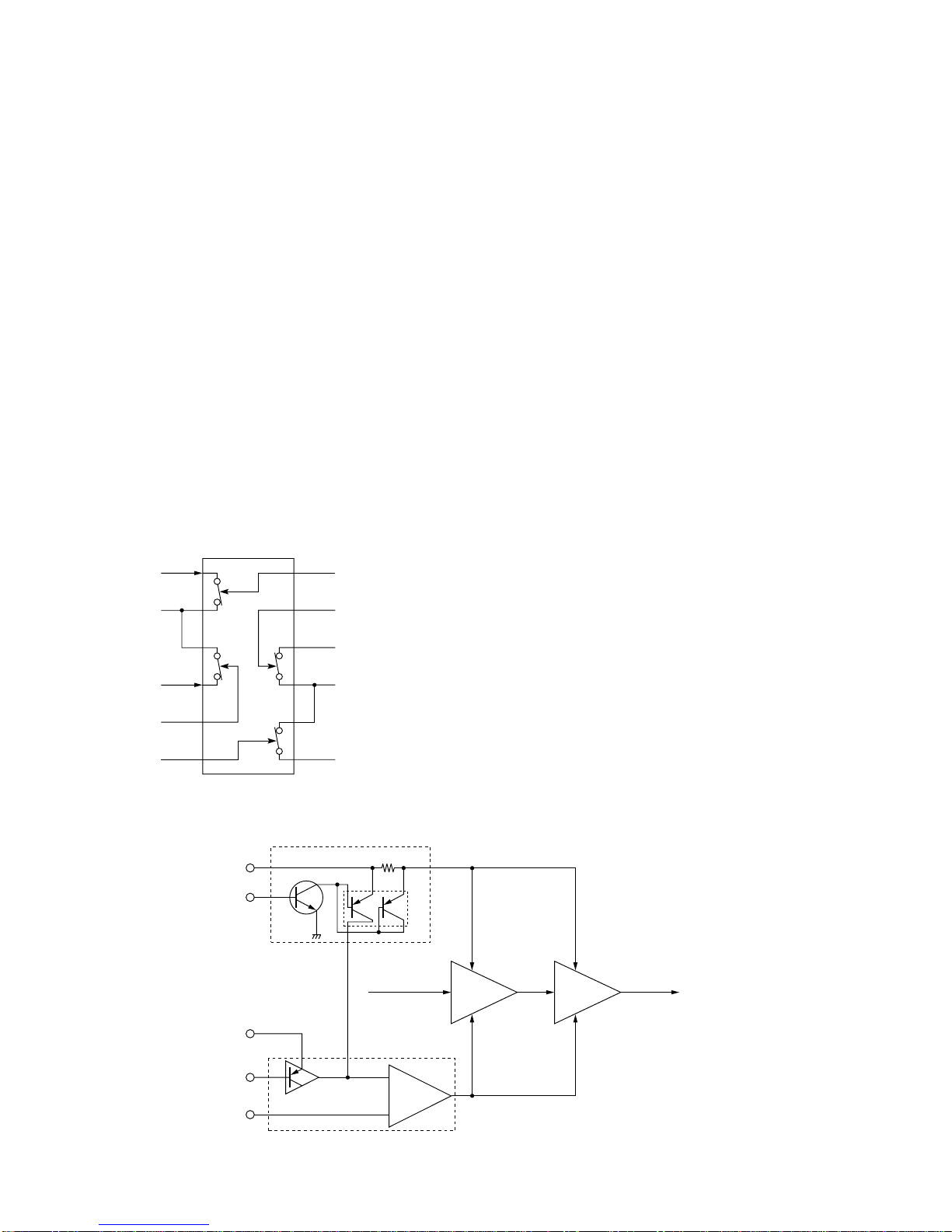
4-1-1 ANTENNA SWITCHING CIRCUIT
Received signals passed through the low-pass filter (L1–L3,
C1–C7). The filtered signals are applied to the λ/4type
antenna switching circuit (D8, D32, L15, L16, C76–C78).
The antenna switching circuit functions as a low-pass filter
while transmitting. However, its impedance becomes very
high while D8 and D32 are turned ON. Thus transmit signals
are blocked from entering the receiver circuits. The antenna
switching circuit employs a λ/4type diode switching system.
The passed signals are then applied to the RF amplifier cir-
cuit.
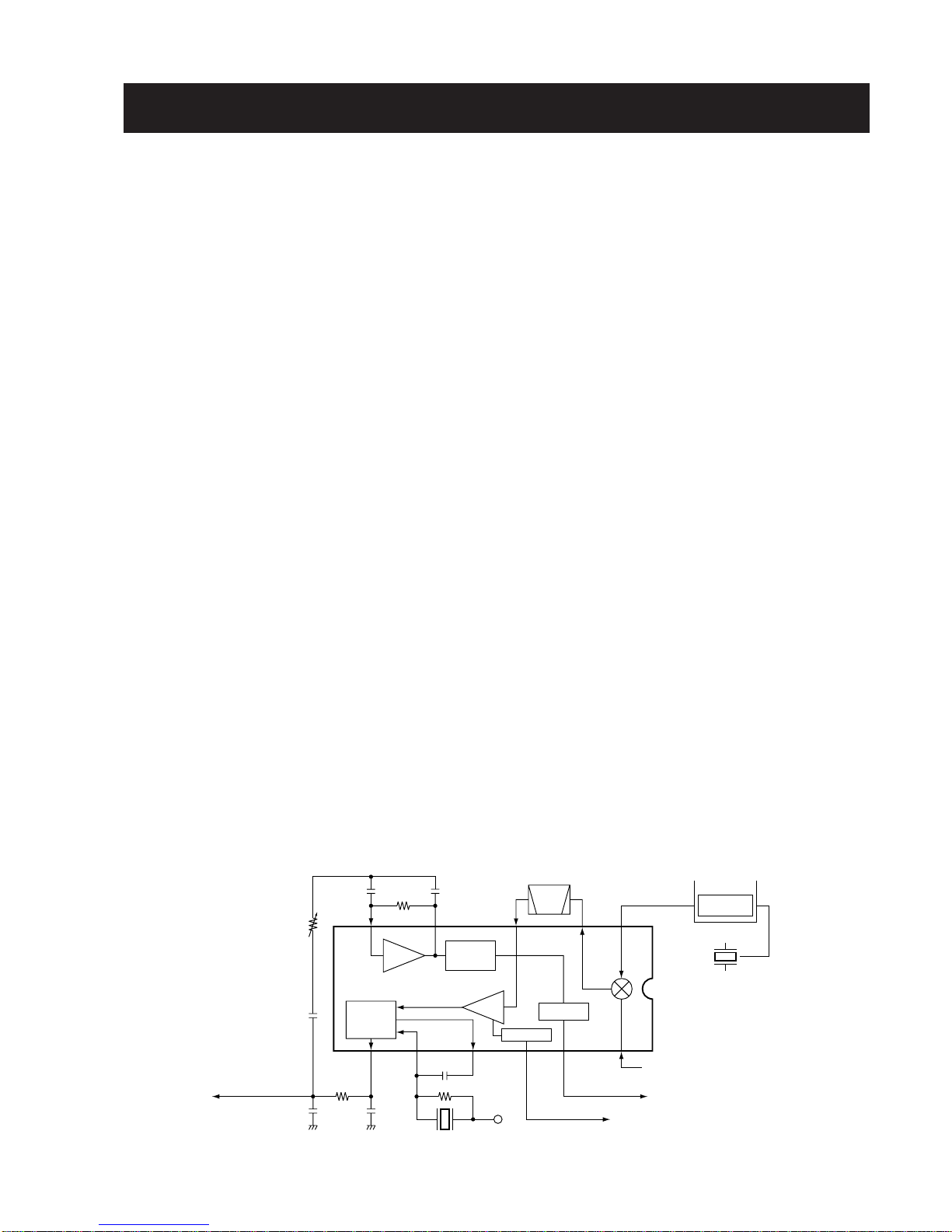
4-1-2 RF CIRCUIT
The RF circuit amplifies signals within the range of frequen-
cy coverage and filters out-of-band signals.
The signals from the antenna switching circuit pass through
a bandpass filter (D10, L26) after being amplified at the RF
amplifier (Q29). The filtered signals are amplified at another
RF amplifier (Q12), then applied to the 1st mixer circuit after
out-of-band signals are suppressed at the bandpass filter
(D11, D12, L18, L19, C92, C94, C96, C236).
D10–D12 employ varactor diodes that track the bandpass fil-
ters and are controlled by the T4/PWR signal from the CPU
(IC8, pins 54–59). These diodes tune the center frequency of
an RF passband for wide bandwidth receiving and good
image response rejection.
4-1-3 1ST MIXER AND 1ST IF CIRCUITS
The 1st mixer circuit converts the received signal to a fixed
frequency of the 1st IF signal with a PLLoutput frequency. By
changing the PLL frequency, only the desired frequency will
pass through a crystal filter at the next stage of the 1st mixer.
The signals from the RF circuit are mixed at the 1st mixer
(Q13) with a 1st LO signal coming from the VCO circuit to
produce a 30.85 MHz 1st IF signal.
The 1st IF signal is applied to a crystal filter (FI1) to suppress
out-of-band signals. The filtered 1st IF signal is applied to the
IF amplifier (Q14), then applied to the 2nd mixer circuit (IC2,
pin 16).
4-1-4 2ND IF AND DEMODULATOR CIRCUITS
The 2nd mixer circuit converts the 1st IF signal to a 2nd IF
signal. A double conversion superheterodyne system (which
converts receive signal twice) improves the image rejection
ratio and obtains stable receiver gain.
The 1st IF signal from the IF amplifier is applied to the 2nd
mixer section of the FM IF IC (IC2, pin 16), and is mixed with
the 2nd LO signal to be converted to a 450 kHz 2nd IF sig-
nal.
The FM IF IC contains the 2nd mixer, limiter amplifier, quad-
rature detector and active filter circuits. A 30.4 MHz 2nd LO
signal is produced at the PLLcircuit by doubling it’s reference
frequency.
The 2nd IF signal from the 2nd mixer (IC2, pin 3) passes
through a ceramic filter (FI2) to remove unwanted hetero-
dyned frequencies. It is then amplified at the limiter amplifier
(IC2, pin 5) and applied to the quadrature detector (IC2, pins
10, 11) to demodulate the 2nd IF signal into AF signals.
4-1-5 AF CIRCUIT
TheAF amplifier circuit amplifies the demodulatedAF signals
to drive a speaker.
AF signals from the FM IF IC (IC2, pin 9) are applied to the
analog switch (IC4, pin 1) via the AF filter circuit (IC3b, pins
6, 7). The output signals from pin 11 are applied to the AF
power amplifier (IC5, pin 4) after passing through the [VOL]
control (VR board, R1).