QRPKits The Survivor User manual

“The Survivor”
A 80 meter QRP SSB transceiver
●Up to ~ 8 watts pep @ 13.8V +/- 50 kHz.
●0.2 uV receiver sensitivit
●Up to 350 kHz receiver tuning range
●8 ohm 500 mw speaker output.
●“Tune” and CW modes
●50 ma Rx current (with optional Digital Dial)
●small size 6” x 4” x 1.5”, 11.5oz.
●13.8V at 2A min recommended power suppl
Yahoo user group at hendricks_SSB
Manual revised 2-28-16
Operation:
Controls: Controls consist of Volume, Fine and Main (course) tuning.
Volume:
Set the volume control to a comfortable listening level. The AGC ill hold the audio level to this volume for all but the eakest signals. The
AGC has a slightly delayed response to keep it from overshooting hen a large signal appears. This results in a momentary “thump”. Without
the slight delay, all audio ould be lost until the AGC could recover from overshooting, hich could take several seconds.
Main tuning:
Main tuning has about a 350 kHz range in a single turn of the knob. This much range is a bit touchy to tune in a signal, so main tuning is
augmented by a fine tuning control. NOTE: Tuning is “back ards”. Turning the tuning knob clock ise decreases frequency.
Fine tuning:
The fine tuning control has about a 30 kHz range, allo ing you to tune bet een several near-by stations and to compensate for any minor
drift the VFO has during operation.
Microphone: An “electret” microphone element is required. The rig supplies the po er needed for the mic. A suitable, lo cost microphone is
available from .QRPKITS.com
Push To Talk (PTT):
Transmitting is initiated by pushing the PTT button on the microphone and then talking (duh). The PTT s itch is also used to activate “tune”
and “CW” modes.
Tune up mode:
Most 80 meter antennas have a fairly narro band idth so therefore require an antenna tuner hich needs to be readjusted every so often
as you move up or do n the band. Since a steady carrier orks better then histling into the mike to get a signal, a steady carrier or “tune
mode” is built into the rig.
Tune mode is activated by:
1. A very short push and release of the PTT s itch on the microphone, < 1/2 second.
2. A “beep” ill sound in the audio output, announcing the tune mode is no active.
3. Using the PTT ill no activate a 600 Hz tone hich is injected into the microphone circuit to modulate the rig. The tone is also
heard in the speaker hen the rig is transmitting. Transmit po er is typically about 5 atts in tune mode, but ill vary depending
on the microphone gain setting.
4. To exit Tune mode, perform another very short push and release the PTT s itch.
5. A double beep ill sound in the audio output to announce the tune mode is no longer active.
CW [Morse] mode:
The Survivalist can be operated in CW mode thanks to the Tune mode and microprocessor control of the T/R sequencing in the transceiver.
The difference bet een CW and Tune mode is that in CW mode, the transceiver must respond to quick changes in the state of the PTT
s itch and stay in the CW mode. Once enabled, CW mode can only be cleared by turning the rig off, then back on again.
CW mode is enabled by keying the character “H” ith the PTT at bet een 5 and 20 pm. This allo s activating CW mode ith either a
straight key or external paddle. There ill be no annunciating side tone until CW mode is enabled, so you have to mentally count the key
taps to enter the mode. If not enough pulses are detected, the rig may enter Tune mode instead of CW mode. There just has to be four on/off
pulses detected in less than ½ second to enter CW mode. When CW mode is detected and enabled, the audio output ill annunciate “CW”.
The Survivalist ill no operate as a CW transceiver, allo ing for cross mode communication in the phone band.
1 Manual revised 20160229

Parts placement diagram, color coded.
Mostly completed board. The picture illustrates ho a ell constructed board should look like.
2 Manual revised 20160229
Picture 1, mostly assembled board

Parts list:
QTY VALUE Markings/type
2 5.6 ohms GR /BLU/GLD/GLD All resistors are 1/4w, 5% CARBO FILM
2 10 ohms BR /BLK/BLK/GLD
1 51 ohms GR /BR /BLK/GLD this value is easy to mix up with 1 Meg – same colors, reverse
order.
6 100 ohms BR /BLK/BR /GLD
3 220 ohms RED/RED/BR /GLD
12 1 K BR /BLK/RED/GLD
6 10 K BR /BLK/ORG/GLD
3 22 K RED/RED/ORG/GLD
2 47 K YEL/VOL/ORG/GLD
13 100 K BR /BLK/YEL/GLD
1 1MEG BR /BLK/GR /GLD
2 2 K trimmer 6mm
1 10 K Panel mount with switch
1 50 K or 100 K Panel mount control, 12 mm
1 8.2 uHy GRY/RED/GLD/GLD - RFC
1 120 mHy 124 Larger black cylinder
2 10.7 IF cans
1 Poly-variable Tuning cap
1 70 pfd Brown trimmer cap
11 39 pfd 39 PO disk
5 150 pfd 151 C0G MLCC
3 330 pfd 331 disk or MLCC
5 680 pfd 100V 681 C0G MLCC
3 0.001 uFd 102 disk
1 1200 pfd 100V 122 mono 100V C0G
27 0.1 uFd 104 X7R 50V MLCC
2 0.1 uFd 100V 104 FILM, BOX
5 1 ufd / 50V ALUM Electrolytic
4 2.2 ufd /50V Alum electrolytic
1 4.7uFd/25V Alum electrolytic
3 47 uFd/16V Alum electrolytic
1 330 ufd/16V Alum electrolytic
1 RED LED T1
2 J-176 P-channel j-fet TO-92
1 2 3906 P P TO-92
2 2 3819 -channel j-fet TO-92
8 2 3904 P TO-92
4 2 7000 MOSFET TO-92
1 FQ 1 50CTA 500V MOSFET TO-92
1 IRF510PBF Power mosfet TO-220
1 78L05 5V, 100 ma regulator
2 1 4148 SS diode
2 1 5231B 5.1V zener
3 Manual revised 20160229

1 1 4756B 47 V 1W zener
1 1 5817 1A shottky diode
2 SA612A 8 pin DIP mixer/osc
1 LM358 8 pin DIP dual op amp
2 LM386 8 pin DIP Audio amp
1 74HC4053 16 pin DIP multiplexer
1 ATTI Y13A 8 pin DIP Atmel processor
6 8 pin DIP socket
1 16 pin DIP socket
6 9.000 MHz, series HU-49US crystal matched
1 FT50-43 Black, Ferrite core, large
1 FT37-43 Black, ferrite core, small
2 T50-2 Red powered iron core
1 T50-7 White powered iron core
1 2.1 mm Power Jack, PC mount
2 Stereo panel jack
1 B C panel jack
1 TO-220 insulator Mica
1 #4, 1/2” ylon screw
1 #4 nut for above
1 Main PCB
1 Case, top
1 Case, bottom
1 Red film
2 Small knob
1 Large knob
1 Tilt stand bale
2 Bale mounting blocks
4 Rubber feet
7 # 4-40 1/4” pan head screws
2 # 4-40 1/4” flat head screws
1 5 feet Insulated hook up wire, #24
1 5 feet #24 magnet wire
1 2 feet #28 magnet wire
4 Manual revised 20160229

Print this large, ink jet printer friendly parts placement and value diagram for easy reference during assembly.
Experienced builders ill likely only need this diagram to stuff most of the board, but revie the assembly
instructions for any notes.
5 Manual revised 20160229

Assembl tips:
●Presort the various parts and place similar types in small paper picnic bo ls. Resistors in one, capacitors in another, and so on.
This ill not only speed assembly, but ill also help keep parts from getting lost. If you like, you can also cross check the parts
against the parts list as you do this to make sure you have them all.
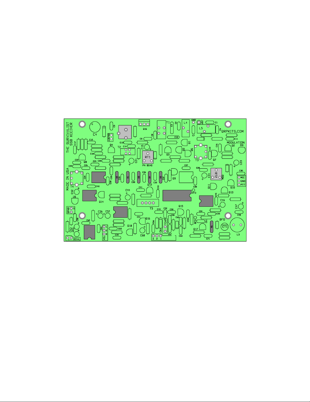
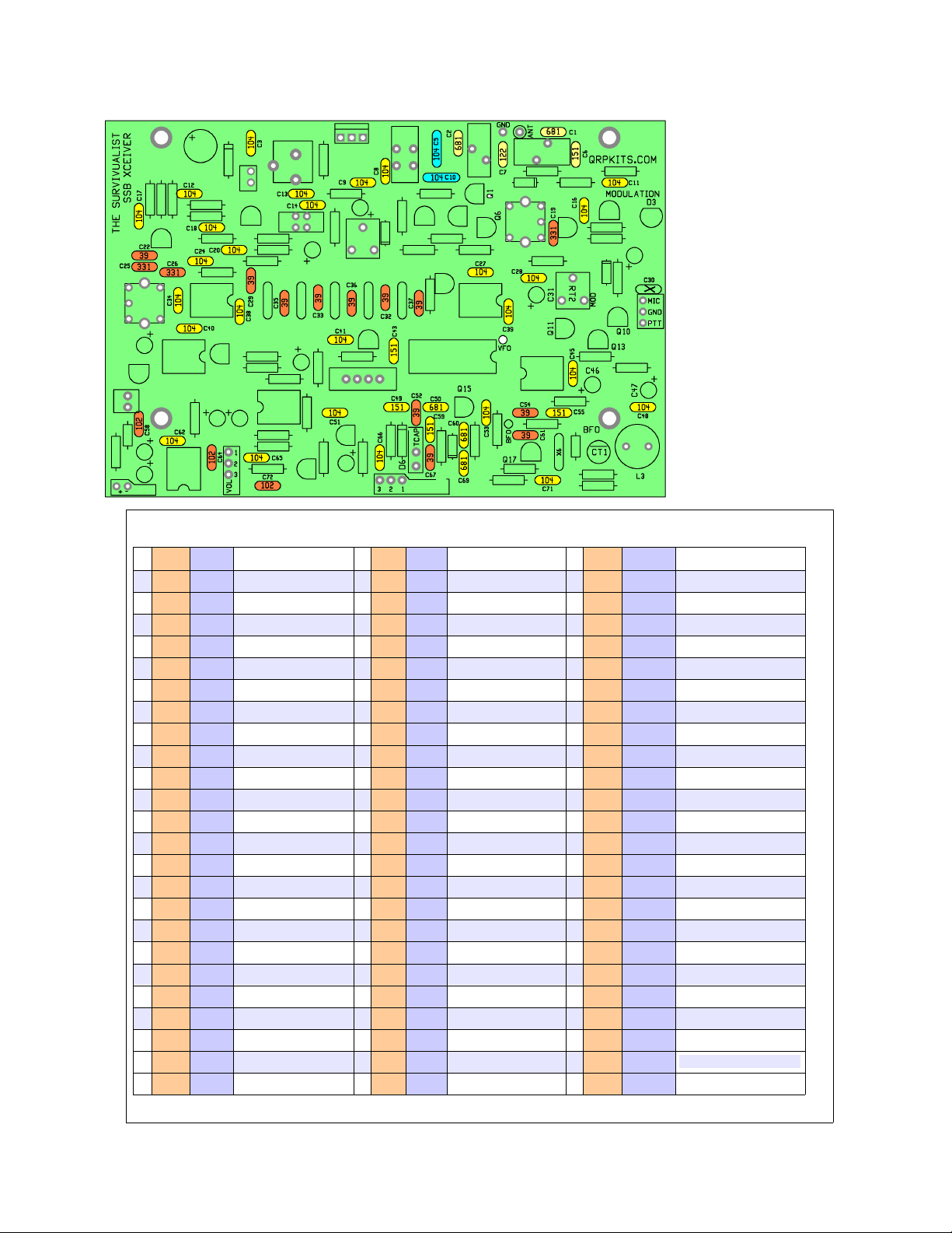
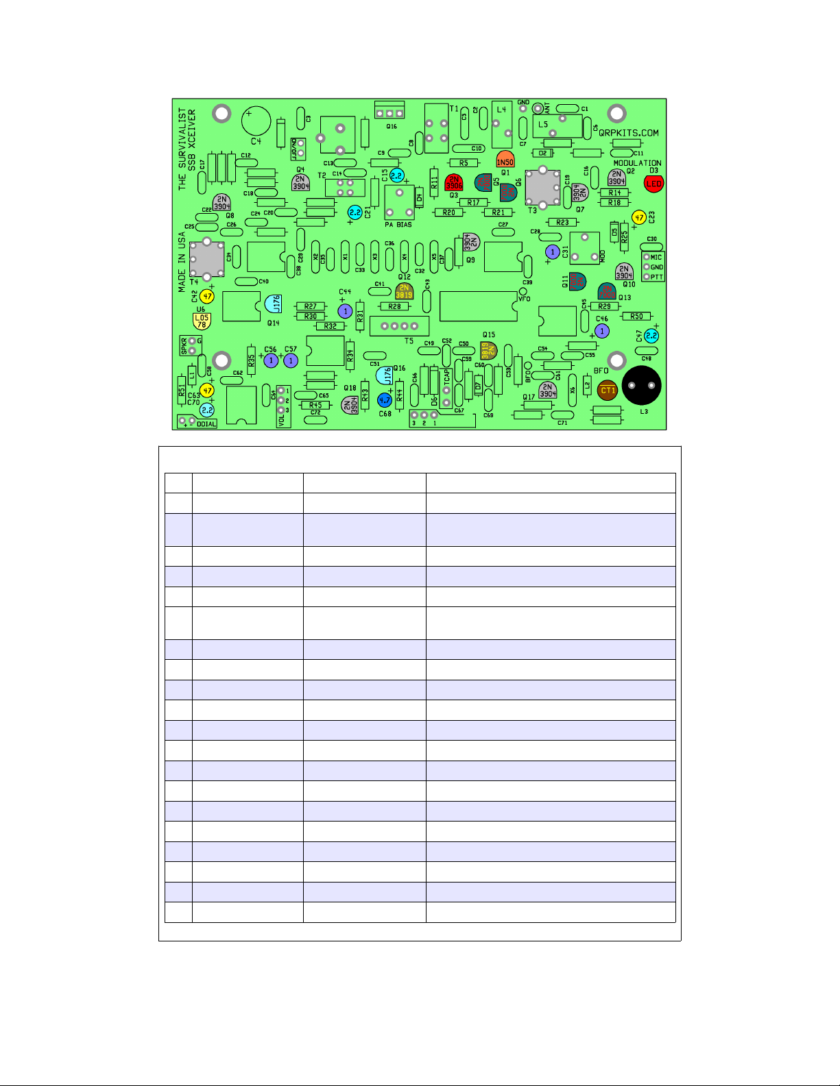
● Be sure to print out the black and hite parts placement diagram as this ill be easier to reference most of the time. You really
don't have to print out the hole manual if you have a laptop or equivalent on your orkbench to vie this.
●Hopefully you already kno ho to solder and don't need to be told to heat both the component lead and the solder pad ith the
tip of the soldering iron. Be stingy ith the solder. You don't need much, only enough to fill up the hole. Using 0.020” diameter
solder allo s better control then the more common 0.032”.
●The circuit board is assembled in the order of parts height. Lo profile parts starting ith resistors are installed first, the
progressively taller parts are added.
●Q16, the transmitter output transistor ill be the very last part mounted and only after the board has been ired into the case and
tested.
●If you bought the Digital Dial option, it ould be a good idea to built and calibrate this first. The Digital Dial can be used to adjust
the VFO coil to put the tuning into the proper range.
Cabinet prep:
●There is a “Modulation” indicator LED on the board, hich you might ant to bring out to the front panel. This ould require drilling
a small hole someplace on the front, hich ould best be done no .
●If desired, paint the cabinet.
●Tape the red film over the display cutout on the front panel. If you'll be using the optional Digital Dial, snip the corner of the film to
uncover the s itch hole.
●Attach the tilt bail to the bottom of the case and add the four rubber feet bumpers.
●Attach the decals as described belo .
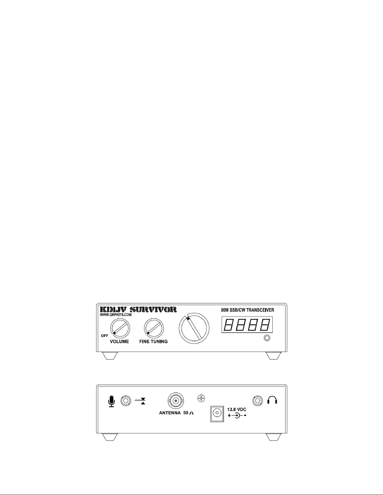
The decals are applied the same as model decals. Cut around each group of text or symbols you ish to apply. It doesn’t have to be perfect
as the background film is transparent. Apply the decals before you mount anything to the chassis. Use the above picture to get the correct
spacing around the holes and cutouts, as it is very easy to do a great decal installation and have a portion covered up ith a knob
Thoroughl clean the surface of the panel to remove an oils or contamination. We have found that moving the decals into
position on bare aluminum chassis is difficult, due to the brushed surface, so we advise pre-coating the chassis with the Kr lon
clear before appl ing the decals, and then, after as well.
Trim around the decal. After trimming, place the decal in a bo l of luke arm ater, ith a small drop of dish soap to reduce the surface
tension, for 10-15 seconds. Using t eezers, handle carefully to avoid tearing. Start to slide the decal off to the side of the backing paper, and
place the unsupported edge of the decal close to the final location. Hold the edge of the decal against the panel, ith your finger, and slide
the paper out from under the decal. You can slide the decal around to the right position, as it ill float slightly on the film of ater. Use a knife
point or something sharp to do this. When in position, hold the edge of the decal ith your finger and gently squeegee excess ater out from
under the decal ith a tissue or paper to el. Work from the center, to both sides. Remove any bubbles by blotting or iping gently to the
sides. Do this for each decal, and take your time. Allo to set overnight, or speed drying by placing near a fan for a fe of hours. When dry,
spray t o light coats of matte finish, Krylon, clear to seal and protect the decals, and allo to dry in bet een coats. All decals come ith t o
complete sets, in case you mess one up.
6 Manual revised 20160229

Resistor, RFC and Diode placement
Caution: The 1N4148 and 1N5231
diodes look identical, read the
numbers carefully on the side of the
part. A magnifying glass maybe
required. Observe polarity as
indicated by black line on one end
of the part and diagram.
Parts are numbered on the board
from left to right, top to bottom in
diagonal ro s.
Sorting the resistors into their
various values before hand ill
speed up assembly.
You may ant to install all the
resistors of one value at a time
instead of sequential locations.
BLK = Black = 0
BRN = Bro n = 1
RED = Red = 2
ORG = Orange = 3
YEL = Yello = 4
GRN = Green =5
BLU = Blue = 6
VOL = Violet = 7
GRY = Gray = 8
WHT = White = 9
7 Manual revised 20160229
√ LOC Value Color code √LOC Value Color code √LOC Value Color code
R1 10 BR /BLK/BLK/GLD R2 100K BR /BLK/YEL/GLD R3 10K BR /BLK/ORG/GLD
R4 100K BR /BLK/YEL/GLD R5 10K BR /BLK/ORG/GLD R6 1K BR /BLK/RED/GLD
R7 220 RED/RED/BR /GLD R8 10K BR /BLK/ORG/GLD R9 22K RED/RED/ORG/GLD
R10 5.6 GR /BLU/GLD/GLD R11 100K BR /BLK/YEL/GLD R12 51 GR /BR /BLK/GLD
R13 5.6 GR /BLU/GLD/GLD R14 1K BR /BLK/RED/GLD R15 220 RED/RED/BR /GLD
R16 10K BR /BLK/ORG/GLD R17 1K BR /BLK/RED/GLD R18 1K BR /BLK/RED/GLD
R19 47K YEL/VOL/ORG/GLD R20 1K BR /BLK/RED/GLD R21 1K BR /BLK/RED/GLD
R22 100 BR /BLK/BR /GLD R23 1K BR /BLK/RED/GLD R24 1K BR /BLK/RED/GLD
R25 22K RED/RED/ORG/GLD R26 1K BR /BLK/RED/GLD R27 22K RED/RED/ORG/GLD
R28 10K BR /BLK/ORG/GLD R29 100 BR /BLK/BR /GLD R30 100K BR /BLK/YEL/GLD
R31 100K BR /BLK/YEL/GLD R32 100K BR /BLK/YEL/GLD R33 100 BR /BLK/BR /GLD
R34 100K BR /BLK/YEL/GLD R35 10 BR /BLK/BLK/GLD R36 220 RED/RED/BR /GLD
R37 100 BR /BLK/BR /GLD R38 1K BR /BLK/RED/GLD R39 100K BR /BLK/YEL/GLD
R40 1K BR /BLK/RED/GLD R41 100K BR /BLK/YEL/GLD R42 100K BR /BLK/YEL/GLD
R43 1K BR /BLK/RED/GLD R44 1 M BR /BLK/GR /GLD R45 100K BR /BLK/YEL/GLD
R46 100K BR /BLK/YEL/GLD R47 100K BR /BLK/YEL/GLD R48 100 BR /BLK/BR /GLD
R49 10K BR /BLK/ORG/GLD R50 47K YRL/VOL/ORG/GLD R51 100 BR /BLK/BR /GLD
D1 1 5817 D2 1 4148 D3 Install later (LED)
D4 1 5231B D5 1 5231B D6 1 4756B
D7 1 4148
L1 8.2 u GRY/RED/GLD/GLD L2 0 Wire jumper
Note: L2 is wire jumper.

Sockets, crystals, trimmer resistors and DC po er connector:
●Parts to be installed are highlighted in gray in diagram belo .
●Install crystals. Push flush to board.
○Solder end of X1 through X5 to solder pad at the top of can. NOTE: leaving a gap bet een the crystal case and the board
can allo solder to flo under the case and short out the lead.
●Install the IC sockets.
○The notch on one end of the socket should be at the same end of the part outline hich also has the notch. Note that not all
the sockets face the same direction.
○Make sure all the pins are sticking through the holes in the board before you start to solder. Sometimes a pin ill fold over
under the socket as it is inserted. If this happens and is not noticed, it can be very difficult to remove the socket to fix once
you start soldering.
●Install the t o trimmer resistors. They ill go in easier if you first flatten out the kink in the leads ith your pliers.
●Install the DC po er jack.
8 Manual revised 20160229

Ceramic capacitors
Electrolytic caps are installed
later, their values are left blank
on the chart belo .
The numbers on the small MLCC
(Multilayer Ceramic Capacitors)
can be hard to read. A
magnifying glass is
recommended. You don't ant to
mix up the values, as that could
lead to problems not easily
found.
9 Manual revised 20160229
√ LOC Value code/type √LOC Value code/type √LOC Value code/type
C1 680 p 681 MLCC C0G C2 680 p 681 MLCC C0G C3 0.1 u 104 MLCC X7R
C4 ------------ C5 0.1 u 104 FILM, BOX blue C6 150 p 151 MLCC C0G
C7 1200p 122 MLCC C0G C8 0.1 u 104 MLCC C9 0.1 u 104 MLCC
C10 0.1 u 104 FILM BOX blue C11 0.1 u 104 MLCC C12 0.1 u 104 MLCC
C13 0.1 u 104 MLCC C14 0.1 u 104 MLCC C15 -----------
C16 0.1 u 104 MLCC C17 0.1 u 104 MLCC C18 0.1 u 104 MLCC
C19 330 p 331 DISK C20 0.1 u 104 MLCC C21 -----------
C22 39 p 39 DISK C23 ---------------- C24 0.1 u 104 MLCC
C25 330 p 331 DISK or MLCC C26 330 p 331 DISK or MLCC C27 0.1 u 104 MLCC
C28 0.1 u 104 MLCC C29 39 p 39 DISK C30 OT USED
C31 --------------- C32 39 p 39 DISK C33 39 p 39 DISK
C34 0.1 u 104 MLCC C35 39 p 39 DISK C36 39 p 39 DISK
C37 39 p 39 DISK C38 0.1 u 104 MLCC C39 0.1 u 104 MLCC
C40 0.1 u 104 MLCC C41 0.1 u 104 MLCC C42 -----------
C43 150 p 151 MLCC C0G C44 --------------- C45 0.1 u 104 MLCC
C46 -------------- C47 ---------------- C48 0.1 u 104 MLCC
C49 150 p 151 MLCC C0G C50 680 p 681 MLCC C51 0.1 u 104 MLCC
C52 39 p 39 DISK C53 0.1 u 104 MLCC C54 39 p 39 DISK
C55 150 p 151 MLCC C0G C56 -------------- C57 -------------
C58 1000p 102 DISK C59 150 p 151 MLCC C0G C60 680 p 681 MLCC
C61 39 p 39 DISK C62 0.1 u 104 MLCC C63 --------------
C64 1000p 102 DISK C65 0.1 u 104 MLCC C66 0.1 u 104 MLCC
C67 39 p 39 DISK C68 ------------- C69 680 p 681 MLCC
C70 --------------- C71 0.1 u 104 MLCC C72 1000p 102 DISK

TO-92 transistors and odds and ends:
10 Manual revised 20160229
√ location value
Q1 1N50 1 place , orange
Q2, 4, 7, 8, 9, 10, 17,
18
2N3904 8 places, gray
Q3 2N3906 1 place, red
Q5, 6, 11, 13 2N7000 4 places, teal
Q12, 15 2N3819 2 places, olive
Q14, Q16 J-176 2 places, light blue (Q16 number as accidentally
duplicated at top of board for IFR510B)
U6 78L05 Pale yello
C31, 44, 46, 56, 57 1 ufd/ 50 V Aluminum Electrolytic – Long lead is Plus
C15, 21, 47, 70 2.2 ufd / 25V Aluminum Electrolytic – Long lead is Plus
C68 4.7 ufd / 25 or 16V Aluminum Electrolytic – Long lead is Plus
C23, 42, 63 47 ufd / 16V Aluminum Electrolytic – Long lead is Plus
C4 330 ufd / 16V Aluminum Electrolytic – Long lead is Plus
T3, T4 IF can
CT1 Bro n trimmer cap Flat side of cap goes to ards line on board.
L3 120 mHy inductor Large black cylinder “124” marked on top.
D3 Red LED Long lead goes into hole on round side of outline.

Toroidal coils:
No the fun part – inding the toroidal coils.
Picture 2 sho s properly ound coils. Note ho the ire is made to
conform closely to the core. Winding the ire loosely around the core
is not only sloppy, but ill not ork properly. Ho ever, you don't ant
the ire to be too tight, just snug.
Before inding the ire on the hite core used for the VFO, it helps to
stretch the ire slightly by grabbing both ends ith pliers and giving
them a little tug.
Coils sho n left to right: VFO coil, Bifilar T1, LPF coil L4
Picture 3 sho s ho the ire ends need to be trimmed back and tinned before the coil is inserted into
the board. Putting a little blob of solder on the tip of your iron and then gently rubbing it against the ire
ill melt through the insulation and tin the ire.
Trying to solder to the ire after it has been inserted into the board holes ithout tinning ill not ork,
as the pad and connecting tracks ill ick a ay too much heat. Using enough heat to melt through the
insulation in that case can damage the board. A common mistake is to tin the ire, but not close
enough to core, so hen mounted, the insulated part of the ire is in the hole and not soldered to, hile
the tined part is actually snipped off.
●L4, L5 T50-2 core (large, red) 22 turns, # 24 ire. (14”) Evenly space turns
around core, leaving small gap at ire ends
●T1 – FT50-43 core, (large, black) 5 turns, # 24 ire, bifilar. (8”) Fold ire in half and
lightly t ist together. After inding, snip ire here folded to separate ends. Use
ohm meter to identify the common ends of the t o ires. Arrange the common ends
to be opposite each other on the core as sho n in the diagram to the right.
●T2 – FT37-43 core (small, black) 5 turns, #28 ire, bifilar. (6”) As ith T1, fold ire in
half and ind 5 turns. Identify ire ends and arrange opposite each other as ith T1.
The ires on T1 and T2 are no orientated properly and are symmetrical in respect
to the pad locations on the board. If the ire ends are not properly located, the
transmitter ill not ork.
●Install L4, L5, T1 and T2 as sho n in placement diagram belo . Before placing T1 and T2, double check that the ires going in to
the A-A' pads have continuity ith an ohm meter, indicating they are the ends of the same ire.
●● T5 – T50-7 core (large, hite). Wind 21 turns #24 ire. (14”) This is the primary inding. Next ind 8 turns of
#28 ire (6”) in gap in bet een #24 ire ends. This is the secondary inding. Make the inding snug to the core
for stability, but still loose enough you can move them slightly to adjust the spacing.
●Install T5 the primary inding (21 turns) in the pads labeled “P” and the secondary (8 turns) into the holes
labeled “S”.
11 Manual revised 20160229
Picture 2, wound toroids
Picture 3, tinned wires

Chassis wiring:
Picture 4 sho n belo sho s ho the board to chassis iring should look like. Note that the ires are made long enough so that there is
some slack, but not so long as to be sloppy. Except for the antenna connections, the ires connecting to the real panel are routed along the
side of the board, rather then above and across it.
●Mount the front panel parts first. Tuning cap, RIT and Volume control and Digital Dial. Bend or remove anti-rotation tabs on pots.
●The BNC antenna jack ires from the board should be soldered to the board before the board is mounted into the case.
●You can cut the rest of the ires to length and solder them to the board out side the case, or you can mount the board into the
case and solder the ires on to the board from the top.
●Wire up the front panel controls. Use the #24 magnet ire bet een the board and tuning cap.
●Install the rear panel jacks and ire them up.
●A ground ire isn't required to the Digital Dial as the cabinet acts as the return path, but one can be added bet een the t o boards
at the “G” pad near L3.
Microphone jack is sho n ired so
PTT is tip and mic element is ring.
This allo s using straight key or keyer
ith standard mono phone plug
attached.
12 Manual revised 20160229
Picture 4, chassis wiring
Part to connect # of ires Length
Volume 3 ires 2”
RIT control 3 ires 2.5”
Tuning cap 2 ires 1.5” #24 magnet
DDial p r 1 ire 6”
DDial Freq input 1.75”
DC p r 2 ires 5” (on/off s itch on vol)
Speaker jack 2 ires 4”
Mic jack 3 ires 3”
Antenna 2 ires 1.5”
Note: Jumpering the t o outer tabs on the tuning cap results
in the maximum tuning range.

Testing and alignment:
●Since the rig does not have it's o n internal po er fuse, it is a good idea to use a po er cord ith an in line fuse or a current
limited po er supply hich can be set to 1 amp. If there happens to be a problem during testing, this ill prevent damage to the
board and/or your po er supply.
The first test is to check operation of the VFO and BFO:
This can be done ith an external frequency counter, the digital dial or a general coverage short ave receiver ith external antenna jack
and BFO. If none of these are available, you ill have to assume the frequency range is about right and check it later ith an 80 meter ham
band receiver.
1. Apply po er to the board and turn on.
2. If you have the Digital Dial installed, it should come on.
3. Connect the Digital Dial input or a frequency counter to the test point “VFO”
4. The frequency should be bet een 5.00 and 5.35 MHz depending on the setting of the tuning capacitor.
5. With both the tuning capacitor and RIT control tuned fully counter clock ise, the VFO frequency should be slightly
above 5.000 MHz. 5.000 MHz corresponds to an operating frequency of 4.00 MHz. (9 – 5)
6. The VFO frequency is “t eaked” by adjusting the spacing of the turns on the VFO coil, T5. Moving turns closer together
ill lo er the frequency. If the frequency is already too lo , you ill have to remove a turn from the coil to increase the
frequency.
7. Move the frequency counter to the “BFO” test point and verify a frequency about 9.000 MHz. With the counter at this test
point, no is a good time to set the BFO trimmer, CT1. Using a small slotted scre driver, adjust the trimmer for a BFO
frequency to about 9.003,000 MHz. NOTE: a frequency counter connected to the BFO test pad can load do n the
oscillator so you may not be able to reach 9.003,000 MHz. The BFO frequency can also be found on pin 7 of U1. This is
a buffered signal, so it ill not be affected by the counter probe capacitance loading.
●You can no install all the IC's into the sockets. Pay attention to the orientation, as they don't all face the same direction. The dot
or notch on the part indicates the Pin 1 end and corresponds to the notch in the socket.
1. Connect an antenna and speaker or headphones to rear panel jacks
2. Connect po er cable and turn on.
3. Turn up the volume and you should start to hear band noise or signals hen you tune around. (depends on time of day)
4. If needed, t eak the BFO trimmer for the most natural sounding voice or band noise. You could also connect the audio
output of the rig to your PC running a PSK program like Digipan. The aterfall ill give you a visual indication of the
band idth of the receiver audio.
5. Peak the receiver input transformer, T3. It should peak ith be teen a ½ to full clock ise turn of the slug.
●If you are using the Digital Dial, it can no be set up for direct reading of the operating frequency
1. Connect the frequency input ire to the “BFO” pad on the main board.
2. Tap a short across the “OFFSET SW” pads on the back of the DDial board. The display ill change to read “Lo --”
3. Click the front panel s itch three times to select the “Lo C” mode.
4. Click and hold closed the front panel s itch until the display changes back to numeric characters (should be all zeros).
5. Move the frequency input ire from the “BFO” pad to the “VFO” pad.
6. The dial is no sho ing the operating frequency.
Transmitter testing:
●Set PA BIAS and MOD controls (VR1 and VR2) to full counter clock ise. They come set from the factory at full clock ise.
●Turn rig on.
●Ground PTT input using microphone, straight key or jumper. TIP is PTT if ired as sho n in diagram.
●Check for 5 volts at Anode (banded) end of D4 and D5. (reference iring diagram for location) This is very important!
13 Manual revised 20160229

●If you do not measure 5V at D4 and D5, you have one or both zeners misplaced and are in one of the 1N4148 locations. You ill
no have to determine if the correct diode ended up in location D2 or D7 by trial and error. You have a 50-50 chance of picking the
right one first off. Unless of course, both need to be s apped.
●If you measure 5 volts at D4 and D5, it is no safe to install the Po er Output transistor, Q16 (this of course, is the Q16 next to the
po er jack at the rear of the board)
Installing Q16:
●With the board mounted in the case, install the IRF510B MOSFET at the Q16 location.
●Line up the scre holes and attach ith #4 nylon scre and nut.
●Push the body of Q16 up against the back of the cabinet to slightly kink the leads and ensure it is flush to the case.
●Top solder the three leads to the pads.
●Remove board from case and trim back leads on Q16
●Re-install the board into the case
●Attach Q16 to cabinet ith mica insulator and nylon scre .
●Use an Ohm meter to verify the metal tab of Q16 IS NOT shorted to the case.
Failure to use mica insulator and n lon screw to attach Q16 will result in a short circuit on DC
input.
Transmitter adjustments:
●Connect po er meter if available and dummy load to antenna jack.
●Connect amp meter in series ith po er supply lead, 2 A scale.
●Re-apply po er to the rig.
●Set the Main tuning to about the center of the tuning range.
●Key the microphone (or ground PTT) to enable transmitter.
●Note the current being dra n from the po er supply ith the amp meter.
●Slo ly turn the “PA BIAS” trimmer resistor clock ise, hile atching the amp meter.
●Stop adjusting the BIAS as soon as the current starts to increase.
●Back off on the BIAS just enough to put it belo the threshold of current increase.
●Any higher bias can run the risk of PA oscillations ith non-resistive loads.
●Turn the “MODULATION GAIN” trimmer resistor clock ise to about mid position.
●Activate “TUNE” mode by a short push and release of the PTT s itch. (On time less than ½ second)
●A “Beep” should be heard in the speaker. If not, try again.
●Pushing and holding closed the PTT s itch ill no key the transmitter and insert an audio tone as long as the PTT is pushed.
●Adjust T4 for best po er output as indicated by the po er meter or brightness of the LED mounted on the board. Typically, this ill
be about a ½ to full turn clock ise of the slug in T4.
NOTE: The full po er output band idth of the rig is fairly narro , 100 kHz or so. Therefore, peak T4 in the center of your favorite
slice of 75 meters to operate, such as a regional or local net frequency.
14 Manual revised 20160229

●Exit TUNE mode by dong a short push and release of the PTT s itch. A double beep should sound in the speaker indicating the
mode has been released.
Setting Modulation level:
Modulation level is ideally set using an oscilloscope so that you can vie the modulation envelope. Ho ever, the on board modulation LED
ill give you a good idea.
●Speaking “TEST” into the microphone should make the Modulation indicator LED flash bright and then flicker. If the LED remains
bright and does not seem to “follo ” your voice, the gain is too high. Conversely, it it barely comes on, the gain is too lo .
NOTE: The voltage at the base of Q10 should be about 1.5 volts hen transmitting. If it is higher than about 1.9 volts, this ill cause the
mixer to become unbalanced as the coupling caps charge and transmit a little burst of RF. If it is much belo 1.3 volts, Q10 may not turn on
or the audio signal from the microphone element ill be clipped and distorted.
Due to variations in the type of mic element used, adjusting the value of the bias supply resistor R25 maybe required. Go up one 5% step if
the voltage is too high and go lo er one 5% step if too lo .
Transmit audio qualit :
A common problem is not having the BFO frequency set correctly, typically too lo in frequency. This results in a double sideband output,
ith neither sounding very good. This can happen even if the receiver audio sounds alright. The higher in frequency you can get the BFO
and still have good sounding audio, the better the opposite sideband and carrier suppression ill be. Typically this frequency ill be
9.003,000 MHz. +/- 500 Hz depending on ho the tolerances of the parts hich happen to end up on your board line up ith each other.
Note that if using a near-by receiver to monitor the transmit audio, it ill likely also to be able to hear the USB and carrier component of the
Survivor output signal. The selectivity of the filter in this lo cost rig isn't stellar, so some opposite side band output is to be expected. On air,
this component of the signal is masked by noise for a station any distance a ay.
With that, you should no be able to attempt your first QSO ith the ne rig!
Tuning range options:
When full tuning range is used, (both capacitor sections of main tuning cap in parallel) full po er output ill not be obtained over the full
tuning range, due to the band idth of the transmitter tuned circuit, T4. This is hy T4 should be peaked at the center of the tuning range.
Tuning range can be reduced if desired by using only one of the capacitor sections. Reducing tuning range ill make tuning less “touchy”
and provide more consistent po er output over the tuning range. T eak the spacing of the turns on the VFO coil T5 to set the tuning range
in your desired section of the band.
Microphone options:
The Survivor rig is designed to use a Electret microphone element, hich are commonly used in CB mics, cordless phones and hands free
microphones for cell phones. Electrets elements have a range of voltages needed to operate. Some ork ith as little as 1.5 volts and others
need as much as 5. This rig is designed to use a 3V element, hich is one of the more common operating voltages.
Since the supply for the mic is 5.1 volts, using a 5V element isn't going to ork.
Dynamic microphones elements are not directly compatible. Older CB set often used a Dynamic mic. Dynamics have a lo impedance and
lo output voltage, therefore an external preamp ill be required. I addition, a 2.2K resistor needs to be placed bet een the mic input and
ground to bias Q10 to the proper voltage. A DC blocking cap may also be required, but this is usually included in the preamp output.
Crystal mics ould also need special treatment, but these are so rare these days it's unlikely you ould use one.
15 Manual revised 20160229

Trouble shooting.
999 out of a 1000 times, the reason a ne ly built kit doesn't ork right a ay is due to assembly errors. Parts can be damaged due to
handling and some of the semi-conductors can be susceptible to ESD (Electric Static Discharge), but this is rare. Therefore, a close visual
inspection ill often be all you need to find the problem.
Look for:
●Bad soldering – missing connections and solder shorts. Bad connections to the magnet ire on the coils is a common problem.
Check for continuity.
●Miss placed parts – IC's in the rong socket or facing the rong ay, transistors in the place and so on.
●It can be sometimes difficult to read the number on the little multilayer ceramic caps and therefore easy to get them in the rong
place. Having a 0.1 ufd by-pass cap here a picofarad part should be and visa-versa ill definitely cause something not to ork.
If something doesn't pop right out at you, some actual trouble shooting to identify the problem area is required. Kno ing here to look for a
problem is half the battle. For this you need to do a process of elimination. Finding out hat does ork can lead to finding hat doesn't ork
and then to the solution. For this some test equipment is needed. A voltmeter is need to start and having an Oscilloscope ith hich to trace
and measure the RF signals is a big plus. Most of you ill likely only have the voltmeter to use. The voltage tables belo can help locate a
problem area. Voltages can vary by 10% due to variations in voltmeters and the actual 5V regulator voltage. You only have to orry if
voltages aren't even close.
Voltages measured ith 13.8V DC supply connected.
16 Manual revised 20160229
U1, U2 SA 612 Pin Voltage Pin voltage
1 1.38 8 5.00
2 1.38 7 4.16
3 0 6 4.93
4 3.84 5 3.84
U3 LM386 Pin Voltage Pin voltage
1 1.25 8 1.25
2 0.0 7 2.45
3 0.0 6 5.00
4 0.0 5 2.38
U5 TINY13A Pin Voltage Pin voltage
Rx / Tx 1 4 / 0 8 5.00
2 5 / 0 7 0 / 0
3 0 or 5 6 0 / 5
4 0.00 5 5 /0
U7 LM358 Pin Voltage Pin voltage
1 2.50 8 5.00
2 2.50 7 2.50
3 2.50 6 2.50
4 0.0 5 2.50
U8 LM386 Pin Voltage Pin voltage
1 1.40 8 1.40
2 0.0 7 6.6
3 0.0 6 13.5
4 0.0 5 6.5
U4 74HC4053 Pin Voltage Pin Voltage
1 4.93 16 5.0
2 4.93 15 4.93
3 4.93 14 2.5
4 4.93 13 2.5
5 4.93 12 0
6 0.0 11 4.0 / 0
7 0.0 10 4.96 / 0
8 0.0 9 4.96 / 0
RED = Tx mode voltages
E (S) B (G) C (D)
Q1 1N50CTA 0 / 013.5 / 0 0 / 0
Q2 2N3904 0 / 0 0 / 0 0 / 5.1
Q3 2N3906 13.5 / 13.5 13.4 / 12.7 0 / 13.4
Q4 2N3904 0 / 1.0 0 / 1.7 13.5 / 13.5
Q5 2N7000 0 / 0 0 / 13.5 13.5 / 0
Q6 2N7000 0 / 00 / 513.4 / 0
Q7 2N3904 0 / 00 / 0.7 0 / 0
Q8 2N3904 0 / 2.1 0 / 2.8 0 / 10.3
Q9 2N3904 3.1 / 3.1 3.8 / 3.8 5 / 5
Q10 2N3904 0 / 0.75 0 / 1.4 0 / 5.1
Q11 2N7000 0 / 00 / 00 / 0.75
Q12 2N3819 2.7 / 2.7 0 / 05 / 5
Q13 2N7000 0 / 00 / 00 / 1.4
Q14 J-176 0 / 05 / 5 0 / 0
Q15 2N3819 1.5 / 1.5 -0.7 / -0.7 4.8 / 4.8
Q16 J-176 0 / 05 / 5 2.5 / 2.5
Q17 2N3904 1 / 11.7 / 1.7 4.5 / 4.5
Q18 2N3904 0 / 00 / 0 5 / 5
Q16 IFR510B 0 / 0 0 / ~2.5 13.5 / 13.5

Theor of operation:
The receiver:
The core of the receiver is comprised of t o SA612 active mixers, ith a 5 crystal ladder filter bet een them for selectivity. An analog s itch
routes the VFO and BFO to the appropriate mixer as needed for either receive or transmit.
During receive, the first mixer, U2, combines the input signal ith the Local Oscillator (VFO) to produce an IF frequency of 9 MHz. An emitter
follo er, Q9, buffers the output of the mixer to provide the crystal filter ith a resistive load. This help reduce ripples in the filter response as
seen on the output side.
The output of the crystal filter is also terminated ith a resistive load and drives the input of the second mixer, U1 hich is acting as the
product detector. A 9 MHz crystal oscillator provides the BFO frequency hich mixes the 9 MHz IF do n to audio.
The output of the product detector, U1, is differentially coupled to a LM386 audio amp, U3. This provides an additional 6 dB of gain over
single ended coupling and helps eliminate any common mode signals on the output of the mixer. The '386 provides a voltage gain of 20 ith
a minimum of external parts. A “P” channel J-fet is connected across the input pins to provide AGC action, more on this later.
The output of the first audio gain stage (U3) drives a pair of non-inverting amplifiers (U7) through a 100 K resistor. One of the amplifiers has
a modest voltage gain of 4.5, hile the other has a much higher gain of 100. The output of the lo gain stage (U7a) is the receiver audio.
The high gain stage is used to drive the AGC circuits, hich is comprised of Q18, Q16 and Q14. The ay this orks is Q16 and Q14 are
normally turned off by a positive voltage on their gates hen there is no input signal, allo ing the full amplification of the audio signal by U3
and U7a. When the audio signal on the output of U7b starts to exceed 500 mV, Q18 starts to turn on. That reduces the gate voltage on Q14
and Q16, allo ing them to start turning on. Q14 shunts the signal bet een the input pins of U3 hile Q16 shunts the signal to ground, using
the 100K resistor R31 as a dropping resistor element.
The gain of U7b is such that AGC action keeps the output signal on U7a to be no more than about 50 mV peak. R44, a 1 meg ohm resistor
and C68, a 4.7 ufd cap sets the AGC time constant. R43, a 1 K resistor bet een the time constant and the controlling transistor Q8 slo s
do n the attack time. Without the limiting resistor, the AGC can overshoot, causing a loss of audio until C68 can charge up again.
Originally, only the Q16 shunt to ground as used for AGC. While this as enough to limit the signal to 50 mV, very strong signals ould
cause U3 to saturate and clip, causing a distorted signal. Adding Q14 to reduce the input signal to U3 eliminated this problem.
The audio signal from U7a is routed through one of the analog s itches in U4, the 74HC4053, to provide muting during transmit. The output
of the s itch drives the volume control and then the final audio po er amp, U8 hich is also a LM386. By putting the AGC action before the
volume control, audio level is consistent and is only varied by the volume control.
The Transmitter:
A small microprocessor, U5, controls the transmit / receive s itching. Not only does it simplify T/R control and timing, it allo ed adding the
Tune mode and CW mode features hich ould have been more complex to do in a strictly analog fashion.
When the PTT input goes lo , (grounded), the follo ing sequence of events happen:
1. The audio is muted
2. The VFO and BFO oscillators are s itched bet een the t o mixers. The product detector (U1) is no the transmit mixer hile the
Receiver input mixer (U2) is no the balanced modulator.
3. The transmitter amplifiers are enabled by turning Q3 on via Q6. This also actives the QSK s itch Q1, disconnecting the antenna to
T3, the input tuned circuit. Q7 is also turned on, shorting the output side of T3 so that any transmit signal hich might leak past Q1
is shorted to ground before it can upset the operation of the mixer, hich is no being used as the balanced modulator.
4. The Microphone buffer transistor, Q10, is turned on by releasing the ground on the base via Q13.
No , hen you speak into the microphone, the audio is mixed ith the 9 MHz BFO signal, hich produces a double sideband signal, 9 MHz
+/- the audio frequency, on the mixer output. The crystal filter removes the upper side band (9 MHz + the audio frequencies), leaving only the
desired lo er sideband signal.
The resulting 9 MHz LSB signal is then mixed in U1 ith the VFO to produce the desired operating frequency in the 75 Meter band. The
desired mixer product is selected by the tuned circuit T4 and then amplified by Q8 and Q4 to a suitable level to drive the po er output
MOSFET Q16 ( hich should have been labeled Q19).
Tune and CW mode:
In order to produce a single frequency output from the transmitter, an appropriate 600 Hz tone is injected into the microphone circuit. The
tone is generated by the TINY13A microprocessor and is of course a square ave. The square ave is filtered through a lo pass filter
comprised of R33, C46, L3 and C47 to remove harmonics and generate a nice sin ave to modulate the transmitter. C48 across L3 blocks
the second harmonic, hich ould other ise take a second filter section to effectively remove. When the tone is being generated, Q13 is
turned on hich turns off the microphone so ambient noise isn't picked up by the mic. Q11 is also turned on, connecting the tone to the
modulation level control.
17 Manual revised 20160229

18 Manual revised 20160229

Board layout. “Floating” pads are grounds to ground plain hich is not sho n so that tracks on both sides of the board can be clearly seen.
19 Manual revised 20160229
Table of contents
Other QRPKits Transceiver manuals