IDT 89EBPES24T3G2 User manual

®
January 2008
6024 Silver Creek Valley Road, San Jose, California 95138
Telephone: (800) 345-7015 • (408) 284-8200 • FAX: (408) 284-2775
Printed in U.S.A.
©2008 Integrated Device Technology, Inc.
IDT™89EBPES24T3G2
Evaluation Board Manual
(Eval Board: 18-657-000)

DISCLAIMER
Integrated Device Technology, Inc. reserves the right to make changes to its products or specifications at any time, without notice, in order to improve design or performance
and to supply the best possible product. IDT does not assume any responsibility for use of any circuitry described other than the circuitry embodied in an IDT product. The
Company makes no representations that circuitry described herein is free from patent infringement or other rights of third parties which may result from its use. No license is
granted by implication or otherwise under any patent, patent rights or other rights, of Integrated Device Technology, Inc.
Boards that fail to function should be returned to IDT for replacement. Credit will not be given for the failed boards nor will a
Failure Analysis be performed.
LIFE SUPPORT POLICY
Integrated Device Technology's products are not authorized for use as critical components in life support devices or systems unless a specific written agreement pertaining to
such intended use is executed between the manufacturer and an officer of IDT.
1. Life support devices or systems are devices or systems which (a) are intended for surgical implant into the body or (b) support or sustain life and whose failure to perform,
when properly used in accordance with instructions for use provided in the labeling, can be reasonably expected to result in a significant injury to the user.
2. A critical component is any components of a life support device or system whose failure to perform can be reasonably expected to cause the failure of the life support device
or system, or to affect its safety or effectiveness.
IDT, the IDT logo, and Integrated Device Technology are trademarks or registered trademarks of Integrated Device Technology, Inc.

Notes
EB24T3G2 Eval Board Manual i January 21, 2008
Table of Contents
®
Description of the EB24T3G2 Eval Board
Introduction .....................................................................................................................................1-1
Board Features ...............................................................................................................................1-2
Hardware ................................................................................................................................1-2
Software..................................................................................................................................1-2
Other.......................................................................................................................................1-2
Revision History..............................................................................................................................1-2
Installation of the EB24T3G2 Eval Board
EB24T3G2 Installation....................................................................................................................2-1
Hardware Description .....................................................................................................................2-1
Reference Clocks............................................................................................................................2-1
Power Sources................................................................................................................................2-2
External Power Source...........................................................................................................2-2
PCI Express Analog High Power Voltage Converter..............................................................2-2
PCI Express Analog Power Voltage Converter ......................................................................2-2
PCI Express Transmitter Analog Power Voltage Converter ...................................................2-2
Core Logic Voltage Converter ................................................................................................2-2
3.3V I/O Voltage Regulator.....................................................................................................2-2
Power-up Sequence ...............................................................................................................2-3
Reset...............................................................................................................................................2-3
Fundamental Reset ................................................................................................................2-3
Downstream Reset .................................................................................................................2-3
Boot Configuration Vector...............................................................................................................2-3
SMBus Interfaces............................................................................................................................2-4
SMBus Slave Interface ...........................................................................................................2-4
SMBus Master Interface .........................................................................................................2-5
JTAG Header..................................................................................................................................2-6
Attention Buttons.............................................................................................................................2-6
Miscellaneous Jumpers, Headers...................................................................................................2-7
LEDs ...............................................................................................................................................2-7
PCI Express Connectors.................................................................................................................2-8
EB24T3G2 Board Figure ..............................................................................................................2-10
Software for the EB24T3G2 Eval Board
Introduction .....................................................................................................................................3-1
Device Management Software........................................................................................................3-1
Schematics
Schematics .....................................................................................................................................4-1

IDT Table of Contents
EB24T3G2 Eval Board Manual ii January 21, 2008
Notes

Notes
EB24T3G2 Eval Board Manual iii January 21, 2008
List of Tables
®
Table 2.1 Clock Source Selection .......................................................................................................2-1
Table 2.2 SMA Connectors - Onboard Reference Clock ....................................................................2-2
Table 2.3 External Power Connector - J1 ...........................................................................................2-2
Table 2.4 Downstream Reset Selection .............................................................................................2-3
Table 2.5 Boot Configuration Vector Signals ......................................................................................2-4
Table 2.6 Boot Configuration Vector Switches S7 & S8 (ON=0, OFF=1) ...........................................2-4
Table 2.7 Slave SMBus Interface Connector ......................................................................................2-5
Table 2.8 EEPROM SMBus Address Setting .....................................................................................2-5
Table 2.9 JTAG Connector Pin Out ....................................................................................................2-6
Table 2.10 Attention Buttons ................................................................................................................2-6
Table 2.11 Miscellaneous Jumpers, Headers .......................................................................................2-7
Table 2.12 LED Indicators .................................................................................................................... 2-7
Table 2.13 PCI Express x8 Connector Pinout ......................................................................................2-8

IDT List of Tables
EB24T3G2 Eval Board Manual iv January 21, 2008
Notes

Notes
EB24T3G2 Eval Board Manual v January 21, 2008
List of Figures
®
Figure 1.1 Function Block Diagram of the EB24T3G2 Eval Board ......................................................1-1

IDT List of Figures
EB24T3G2 Eval Board Manual vi January 21, 2008
Notes

Notes
EB24T3G2 Eval Board Manual 1 - 1 January 21, 2008
®
Chapter 1
Description of the EB24T3G2
Eval Board
Introduction
The 89HPES24T3G2 switch (also referred to as PES24T3G2 in this manual) is a member of IDT’s PCI
Express® standard based line of products. It is a PCIe® Base Specification 2.0 compliant (Gen2) 3-port
switch, with 8 serial lanes per port. One x8 upstream port is provided for connecting to the root complex
(RC), and two x8 downstream ports are available for connecting to PCIe endpoints or to another switch.
More information on this device can be found in the 89HPES24T3G2 User Manual.
The 89EBPES24T3G2 Evaluation Board (also referred to as EB24T3G2 in this manual) provides an
evaluation platform for the PES24T3G2 switch. It is also a cost effective way to add PCIe ports (slots) to an
existing system with limited number of PCIe ports/slots. The EB24T3G2 board is designed to function as an
add-on card to be plugged into a x8 PCIe slot available on a motherboard hosting an appropriate root
complex and microprocessor(s). The EB24T3G2 is a vehicle to test and evaluate the functionality of the
PES24T3G2 switch. Customers can use this board to get a headstart on software development prior to the
arrival of their own hardware. The EB24T3G2 is also used by IDT to reproduce system-level hardware or
software issues reported by customers. Figure 1.1 illustrates the functional block diagram representing the
main parts of the EB24T3G2 board.
Figure 1.1 Function Block Diagram of the EB24T3G2 Eval Board
JTAG
Header
Main
Reset
I/O Expander
PCA9555
PCIe x8 Upstream Edge
EEPROM
24LC512
SMBUS
HEADER
PES24T3G2
PCI Express
Switch
External Power
PCIe x8 Downstream Slot
x8
25 MHz Crystal
Clock
Generator
Clock
Fanout
SMBus
PCIe x8 Downstream Slot
Voltages on board
+12V, +3.3V, +2.5V, +1.0V
Connector
Power
Module
PTH08T240
x8
x8
Port 4
Port 2
Port 0
(lane reversed)

IDT Description of the EB24T3G2 Eval Board
EB24T3G2 Eval Board Manual 1 - 2 January 21, 2008
Notes Board Features
Hardware
PES24T3G2 PCIe 3 port switch
– Three x8 ports, 24 PCIe lanes
– PCIe Base Specification Revision 2.0 compliant (Gen2 SerDes speeds of 5 GT/S)
– Up to 2048 byte maximum Payload Size
– Automatic lane reversal and polarity inversion supported on all lanes
– Automatic per port link width negotiation to x8, x4, x2, x1
– Load configuration from an optional serial EEPROM via SMBUS
Upstream, Downstream Port
– One edge connector on the upstream port, to be plugged into a slot with at least x8 capable on a
host motherboard
– Two slot connectors on the downstream ports, for PCIe endpoint add-on cards to be plugged in.
These slot connectors are x8 mechanically but open-ended for card widths greater than x8
(e.g. x16)
Numerous user selectable configurations set using onboard jumpers and DIP-switches
– Source of clock - host clock or onboard clock generator
– Two clock rates (100/125 MHz) from an onboard clock generator
– Boot mode selection
SMBUS Slave Interface (4 pin header)
SMBUS Master Interface connected to the Serial EEPROMs through I/O expander
“Attention” button for each downstream port to initiate a hot swap event on each port
Four pin connector for optional external power supply
Push button for Warm Reset
Several LEDs to display status, reset, power, “Attention”, etc.
One 10-pin JTAG connector (pitch 2.54 mm x 2.54 mm)
Software
There is no software or firmware executed on the board. However, useful software is provided along
with the Evaluation Board to facilitate configuration and evaluation of the PES24T3G2 within host systems
running popular operating systems.
Installation programs
– Operating Systems Supported: Windows2000, WindowsXP, Vista, Linux
GUI based application for Windows and Linux
– Allows users to view and modify registers in the PES24T3G2
– Binary file generator for programming the serial EEPROMs attached to the SMBUS.
Other
A metal bracket is provided to firmly hold in place two endpoints plugged into the EB24T3G2 board.
An external power supply may be required under some conditions.
SMBUS cable may be required for certain evaluation exercises.
SMA connectors are provided on the EB24T3G2 board for clock outputs.
Revision History
January 21, 2008: Initial publication of eval board manual.

Notes
EB24T3G2 Eval Board Manual 2 - 1 January 21, 2008
®
Chapter 2
Installation of the EB24T3G2
Eval Board
EB24T3G2 Installation
This chapter discusses the steps required to configure and install the EB24T3G2 evaluation board. All
available DIP switches and jumper configurations are explained in detail.
The primary installation steps are:
1. Configure jumper/switch options suitable for the evaluation or application requirements.
2. Connect PCI Express endpoint cards to the downstream port PCIe slots on the evaluation board.
3. Make sure that the host system (motherboard with root complex chipset) is powered off.
4. Insert the evaluation board into the host system.
5. Apply power to the host system.
The EB24T3G2 board is typically shipped with all jumpers and switches configured to their default
settings. In most cases, the board does not require further modification or setup.
Hardware Description
The PES24T3G2 is a 24-lane, 3-port PCI Express® switch. It is a peripheral chip that performs PCI
Express based switching with a feature set optimized for high performance applications such as servers
and storage. It provides fan-out and switching functions between a PCI Express upstream port and down-
stream ports or peer-to-peer switching between downstream ports.
The EB24T3G2 has two PCI Express downstream ports, accessible through two x8 connectors. Both
ports are capable of negotiating a x1, x2, x4, and x8 link width. All endpoint cards connected to the
PES24T3G2 must support one of these link widths.
Basic requirements for the board to run are:
–Host system with a PCI Express root complex supporting at least x8 configuration through a PCI
Express x8 or larger slot.
–x1, x2, x4 or x8 PCI Express Endpoint Cards.
Reference Clocks
The PES24T3G2 requires a differential reference clock. The EB24T3G2 derives this clock from a
common source which is user-selectable. The common source can be either the host system’s reference
clock or it can be the onboard clock generator. Selection is made by stuffing resistors as in Table 2.1.
The source for the onboard clock is the ICS841484 clock generator device (U4) connected to a 25MHz
oscillator (Y1). When using the onboard clock generator, the output frequency is fixed at 100MHz, therefore
FSEL0 (S7, bit 8) is On as the default setting.
Clock Configuration Stuffing Option
W6 and W7 Clock Source
Pins 2 and 3 Onboard Reference Clock – Use onboard clock generator
Pins 1 and 2 Upstream Reference Clock – Host system provides clock (Default)
Table 2.1 Clock Source Selection
IDT Installation of the EB24T3G2 Eval Board
EB24T3G2 Eval Board Manual 2 - 2 January 21, 2008
Notes The output of the onboard clock generator is accessible through two SMA connectors located on the
Evaluation Board. See Table 2.2. This can be used to connect a scope for probing or capturing purposes
and cannot be used to drive the clock from an external source.
Power Sources
The EB24T3G2 and both downstream ports are powered from the upstream port slot power. If add-in
cards require more power than the upstream slot can support, an external source is required to supply this
extra power via an auxiliary 4-pin power connector on the board. Header W1, W2, and W3 (see Table 2.11)
are used to select proper power source for the switch and all downstream ports.
External Power Source
If necessary, external power is supplied to the EB24T3G2 board through a 4-pin auxiliary power
connector attached to J4. The external power supply provides +12V to the EB24T3G2 as described in Table
2.3. The +5V is unused.
PCI Express Analog High Power Voltage Converter
A DC-DC converter (U18) provides a 2.5V PCI Express analog high power voltage (shown as VDDHA)
to the PES24T3G2.
PCI Express Analog Power Voltage Converter
A separate DC-DC converter (U16) provides a 1.0V PCI Express analog power voltage (VDDA) to the
PES24T3G2.
PCI Express Transmitter Analog Power Voltage Converter
A separate DC-DC converter (U17) provides a 1.0V PCI Express transmitter analog power voltage
(shown as VDDPETA) to the PES24T3G2.
Core Logic Voltage Converter
A separate DC-DC converter (U15) provides the 1.0V core voltage (VDDCORE) to the PES24T3G2.
3.3V I/O Voltage Regulator
A 12V to 3.3V voltage regulator (VR1) provides the 3.3V I/O voltage (VDDIO) to the PES24T3G2.
Onboard Reference Clock Output (Differential) – J7, J6
J9 Positive Reference Clock
J10 Negative Reference Clock
Table 2.2 SMA Connectors - Onboard Reference Clock
Pin Signal
1+12V
2GND
3GND
4+5V
Table 2.3 External Power Connector - J1

IDT Installation of the EB24T3G2 Eval Board
EB24T3G2 Eval Board Manual 2 - 3 January 21, 2008
Notes Power-up Sequence
During power supply ramp-up, VDDCORE must remain at least 1.0V below VDDIO at all times. There
are no other power-up sequence requirements for the various operating supply voltages.
Reset
The PES24T3G2 supports two types of reset mechanisms as described in the PCI Express specifica-
tion:
–Fundamental Reset: This is a system-generated reset that propagates along the PCI Express
tree through a single side-band signal PERST# which is connected to the Root Complex, the
PES24T3G2, and the endpoints.
–Hot Reset: This is an In-band Reset, communicated downstream via a link from one device to
another. Hot Reset may be initiated by software. This is further discussed in the 89HPES24T3G2
User Manual. The EB24T3G2 evaluation board provides seamless support for Hot Reset.
Fundamental Reset
There are two types of Fundamental Resets which may occur on the EB24T3G2 evaluation board:
–Cold Reset: During initial power-on, the onboard voltage monitor (TLC7733D) will assert the PCI
Express Reset (PERSTN) input pin of the PES24T3G2.
–Warm Reset: This is triggered by hardware while the device is powered on. Warm Reset can be
initiated by two methods:
•Pressing a push-button switch (S1) located on EB24T3G2 board
•The host system board IO Controller Hub asserting PERST# signal, which propagates through
the PCIe upstream edge connector of the EB24T3G2. Note that one can bypass the onboard
voltage monitor (TLC7733D) by moving the shunt from pin 1-2 to pin 2-3 (default) on W4.
Both events cause the onboard voltage monitor (TLC7733D) to assert the PCI Express Reset
(PERSTN) input of the PES24T3G2 while power is on.
Downstream Reset
The PES24T3G2 provides a a choice of either a software-controlled reset for each downstream port
through GPIO pins or a fundamental reset through PERST#. Selection is made by jumpers described in
Table 2.4.
Boot Configuration Vector
A boot configuration vector consisting of the signals listed in Table 2.5 is sampled by the PES24T3G2
during a fundamental reset (while PERSTN is active). The boot configuration vector defines the essential
parameters for switch operation and is set using DIP switches S7 and S8 as defined in Table 2.6.
Port # Jumper Selection
2 W19 [1-2] Software controlled reset through GPIO0
[2-3] Fundamental reset PERST# (default)
4 W18 [1-2] Software controlled reset through GPIO1
[2-3] Fundamental reset PERST# (default)
Table 2.4 Downstream Reset Selection

IDT Installation of the EB24T3G2 Eval Board
EB24T3G2 Eval Board Manual 2 - 4 January 21, 2008
Notes
SMBus Interfaces
The System Management Bus (SMBus) is a two-wire interface through which various system compo-
nent chips can communicate. It is based on the principles of operation of I2C. Implementation of the SMBus
signals in the PCI Express connector is optional and may not be present on the host system. The SMBus
interface consists of an SMBus clock pin and an SMBus data pin.
Note: MSMBADDR and SSMBADDR address pins are not available in the PES24T3G2. The
MSMBADDR address is hardwired to 0x50, and the SSMBADDR address is hardwired to 0x77.
The PES24T3G2 contains two SMBus interfaces: a slave SMBus interface and a master SMBus inter-
face. The slave SMBus interface allows a SMBus Master device full access to all software-visible registers.
The Master SMBus interface provides connection to the external serial EEPROM used for initialization and
the I/O expanders used for hot-plug signals.
SMBus Slave Interface
On the PES24T3G2 board, the slave SMBus interface is accessible through the PCI Express edge
connector as well as a 4-pin header as described in Table 2.7.
Note: The SMBus signals to the PCI Express edge connector is disabled by default. To enable
them, place 0-ohm resistors at locations R160 and R161.
Signal Description
CCLKDS Common Clock Downstream. The assertion of this pin indicates that all downstream
ports are using the same clock source as that provided to downstream devices. This pin is
used as the initial value of the Slot Clock Configuration bit in all of the Link Status Registers
for downstream ports. The value may be overridden by modifying the SCLK bit in the down-
stream port’s PCIELSTS register. Default: 0x1
CCLKUS Common Clock Upstream. The assertion of this pin indicates that the upstream port is
using the same clock source as the upstream device. This pin is used as the initial value of
the Slot Clock Configuration bit in the Link Status Register for the upstream port. The value
may be overridden by modifying the SCLK bit in the P0_PCIELSTS register. Default: 0x1
SWMODE[2:0] Switch Mode. These configuration pins determine the PES24T3G2 switch operating
mode. Default: 0x0
0x0 - Normal switch mode
0x1 - Normal switch mode with Serial EEPROM-based initialization
0x2 through 0x7 - Reserved
Table 2.5 Boot Configuration Vector Signals
Signal Description Default
S8[1] CCLKDS OFF
S8[2] CCLKUS OFF
S7[1] SWMODE[0] ON
S7[2] SWMODE[1] ON
S7[3] SWMODE[2] ON
Table 2.6 Boot Configuration Vector Switches S7 & S8 (ON=0, OFF=1)

IDT Installation of the EB24T3G2 Eval Board
EB24T3G2 Eval Board Manual 2 - 5 January 21, 2008
Notes .
The slave SMBus interface responds to the following SMBus transactions initiated by an SMBus master.
Initiation of any SMBus transaction other than those listed above produces undefined results. See the
SMBus 2.0 specification for a detailed description of the following transactions:
–Byte and Word Write/Read
–Block Write/Read
SMBus Master Interface
Connected to the master SMBus interface are four 16-bit I/O Expanders (PCA9555) and a serial
EEPROM (24LC512). Four I/O Expanders are used as the interface for the onboard hot-plug controllers
(MIC2591B). The lower three bits of the bus address for the I/O Expander0/1/2/4 are fixed as 0x0, 0x1, 0x2
and 0x4, respectively.
The seven bits address for the selected EEPROM device is 0b1010_000 by default and the lower
three bit is configurable using switch S8 as described in 2.8.
Slave SMBus Interface Connector J8
Pin Signal
1N/C
2SCL
3GND
4SDA
Table 2.7 Slave SMBus Interface Connector
S8[3] S8[4] S8[5] Bus Address
OFF OFF OFF 0b111
OFF OFF ON 0b110
OFF ON OFF 0101
OFF ON ON 0b100
ON OFF OFF 0b011
ON OFF ON 0b010
ON ON OFF 0b001
ON ON ON 0b000 (Default)
Table 2.8 EEPROM SMBus Address Setting
IDT Installation of the EB24T3G2 Eval Board
EB24T3G2 Eval Board Manual 2 - 6 January 21, 2008
Notes JTAG Header
The PES24T3G2 provides a JTAG connector J5 for access to the PES24T3G2 JTAG interface. The
connector is a 2.54 x 2.54 mm pitch male 10-pin connector. Refer to Table 2.9 for the JTAG Connector J5
pin out.
Attention Buttons
The PES24T3G2 features three attention buttons, shown in 2.10. Each button corresponds to a partic-
ular port and is used to initiate hot-swapping events.
JTAG Connector J5
Pin Signal Direction Pin Signal Direction
1 /TRST - Test reset Input 2 GND —
3 TDI - Test data Input 4 GND —
5 TDO - Test data Output 6 GND —
7 TMS - Test mode select Input 8 GND —
9 TCK - Test clock Input 10 GND —
Table 2.9 JTAG Connector Pin Out
Button Description
S5 Port 2 Attention Button
S3 Port 4 Attention Button
Table 2.10 Attention Buttons

IDT Installation of the EB24T3G2 Eval Board
EB24T3G2 Eval Board Manual 2 - 7 January 21, 2008
Notes Miscellaneous Jumpers, Headers
LEDs
There are several LED indicators on the EB24T3G2 which convey status feedback. A description of
each is provided in Table 2.12.
Miscellaneous Jumpers, Headers
Ref.
Designator Type Default Description
W1-W3 Header 1-2 Shunted 1-2: 12.0V source from Upstream Port (Default)
2-3: 12.0V source from external power connector
W20 Header Shunted Disable EEPROM Write protect feature (Default)
S6[1] Switch ON ON: Port2, Force hot-plug controller on
OFF: Port2, Power Enable bit controls hot-plug controller
S6[2] Switch ON ON: Port4, Force hot-plug controller on
OFF: Port4, Power Enable bit controls hot-plug controller
W15 Header 2-3 Shunted 2-3: Port 2, +12V source from Upstream port (Default)
1-2: Port 2, +12V source from hot-plug controller
W9 Header 2-3 Shunted 2-3: Port 4, +12V source from Upstream port (Default)
1-2: Port 4, +12V source from hot-plug controller
W16 Header 2-3 Shunted 2-3: Port 2, +3.3V source from Upstream port (Default)
1-2: Port 2, +3.3V source from hot-plug controller
W10 Header 2-3 Shunted 2-3: Port 4, +3.3V source from Upstream port (Default)
1-2: Port 4, +3.3V source from hot-plug controller
W14 Header 2-3 Shunted 2-3: Port 2, +3.3AUX source from upstream port (Default)
1-2: Port 2, +3.3V source from hot-plug controller
W8 Header 2-3 Shunted 2-3: Port 4, +3.3AUX source from upstream port (Default)
1-2: Port 4, +3.3V source from hot-plug controller
Table 2.11 Miscellaneous Jumpers, Headers
Location Color Definition
DS21 Green Port 2: Power-is-good Indicator
DS15 Green Port 4: Power-is-good Indicator
DS20 Green Port 2: Power Indicator
DS14 Green Port 4: Power Indicator
DS19 Yellow Port 2: Attention Indicator
DS13 Yellow Port 4: Attention Indicator
DS18 Green Port 2: Activity Indicator
DS12 Green Port 4: Activity Indicator
DS17 Green Port 2: Linkup Indicator
DS11 Green Port 4: Linkup Indicator
Table 2.12 LED Indicators (Part 1 of 2)

IDT Installation of the EB24T3G2 Eval Board
EB24T3G2 Eval Board Manual 2 - 8 January 21, 2008
Notes
PCI Express Connectors
DS23 Green Port 0: Linkup Indicator
DS24 Green Port 0: Activity Indicator
DS7 Red Port 2: Power Fault Indicator
DS10 Red Port 4: Power Fault Indicator
DS25 Green GPIO8
DS5 Green GPIO9
DS26 Green GPIO10
DS6 Red Port 2: Manual Retention Latch Indicator
DS9 Red Port 4: Manual Retention Latch Indicator
DS8 Green Port 2: Presence Detect Indicator
DS27 Green Port 4: Presence Detect Indicator
Pin Side A Side B
1 +12V 12V power PRSNT1# Hot-Plug presence detect
2 +12V 12V power +12V 12V power
3 RSVD Reserved +12V 12V power
4 GND Ground GND Ground
5 SMCLK SMBus clock JTAG2 TCK (Test Clock) JTAG i/f clk i/p
6 SMDAT SMBus Data JTAG TDI (Test Data Input)
7 GND Ground JTAG TDO (Test Data Output)
8 +3.3V 3.3V power JTAG TMS (Test Mode Select)
9 JTAG1 TRST# (Test/Reset) resets
JTAG i/f
+3.3V 3.3V power
10 3.3Vaux 3.3V auxiliary power +3.3V 3.3V power
11 WAKE# Signal for Link reactivation PERST# Fundamental Reset
Mechanical Key
12 RSVD Reserved GND Ground
13 GND Ground REFCLK+ REFCLK Reference clock
14 PETp0 Transmitter differential REFCLK- (differential pair)
15 PETn0 pair, Lane 0 GND Ground
16 GND Ground PERp0 Receiver differential
17 PRSNT2# Hot-Plug presence detect PERn0 pair, Lane 0
18 GND Ground GND Ground
19 PETp1 Transmitter differential RSVD Reserved
Table 2.13 PCI Express x8 Connector Pinout (Part 1 of 2)
Location Color Definition
Table 2.12 LED Indicators (Part 2 of 2)

IDT Installation of the EB24T3G2 Eval Board
EB24T3G2 Eval Board Manual 2 - 9 January 21, 2008
Notes
Note: These x8 PCI Express connectors comply with the PCIe specification. According to the
PCI Express specification, the PRSNT1# pin should be wired to the farthest available PRSNT2#
pin on the connector. In the EB24T3G2, all PRSNT2# pins are tied together. This allows a board
with a x1 or a x4 width to be installed.
20 PETn1 pair, Lane 1 GND Ground
21 GND Ground PERp1 Receiver differential
22 GND Ground PERn1 pair, Lane 1
23 PETp2 Transmitter differential GND Ground
24 PETn2 pair, Lane 2 GND Ground
25 GND Ground PERp2 Receiver differential
26 GND Ground PERn2 pair, Lane 2
27 PETp3 Transmitter differential GND Ground
28 PETn3 pair, Lane 3 GND Ground
29 GND Ground PERp3 Receiver differential
30 RSVD Reserved PERn3 pair, Lane 3
31 PRSNT2# Hot-Plug presence detect GND Ground
32 GND Ground RSVD Reserved
33 PETp4 Transmitter differential RSVD Reserved
34 PETn4 pair, Lane 4 GND Ground
35 GND Ground PERp4 Receiver differential
36 GND Ground PERn4 pair, Lane 4
37 PETp5 Transmitter differential GND Ground
38 PETn5 pair, Lane 5 GND Ground
39 GND Ground PERp5 Receiver differential
40 GND Ground PERn5 pair, Lane 5
41 PETp6 Transmitter differential GND Ground
42 PETn6 pair, Lane 6 GND Ground
43 GND Ground PERp6 Receiver differential
44 GND Ground PERn6 pair, Lane 6
45 PETp7 Transmitter differential GND Ground
46 PETn7 pair, Lane 7 GND Ground
47 GND Ground PERp7 Receiver differential
48 PRSNT2# Hot-Plug presence detect PERn7 pair, Lane 7
49 GND Ground GND Ground
Pin Side A Side B
Table 2.13 PCI Express x8 Connector Pinout (Part 2 of 2)
IDT Installation of the EB24T3G2 Eval Board
EB24T3G2 Eval Board Manual 2 - 10 January 21, 2008
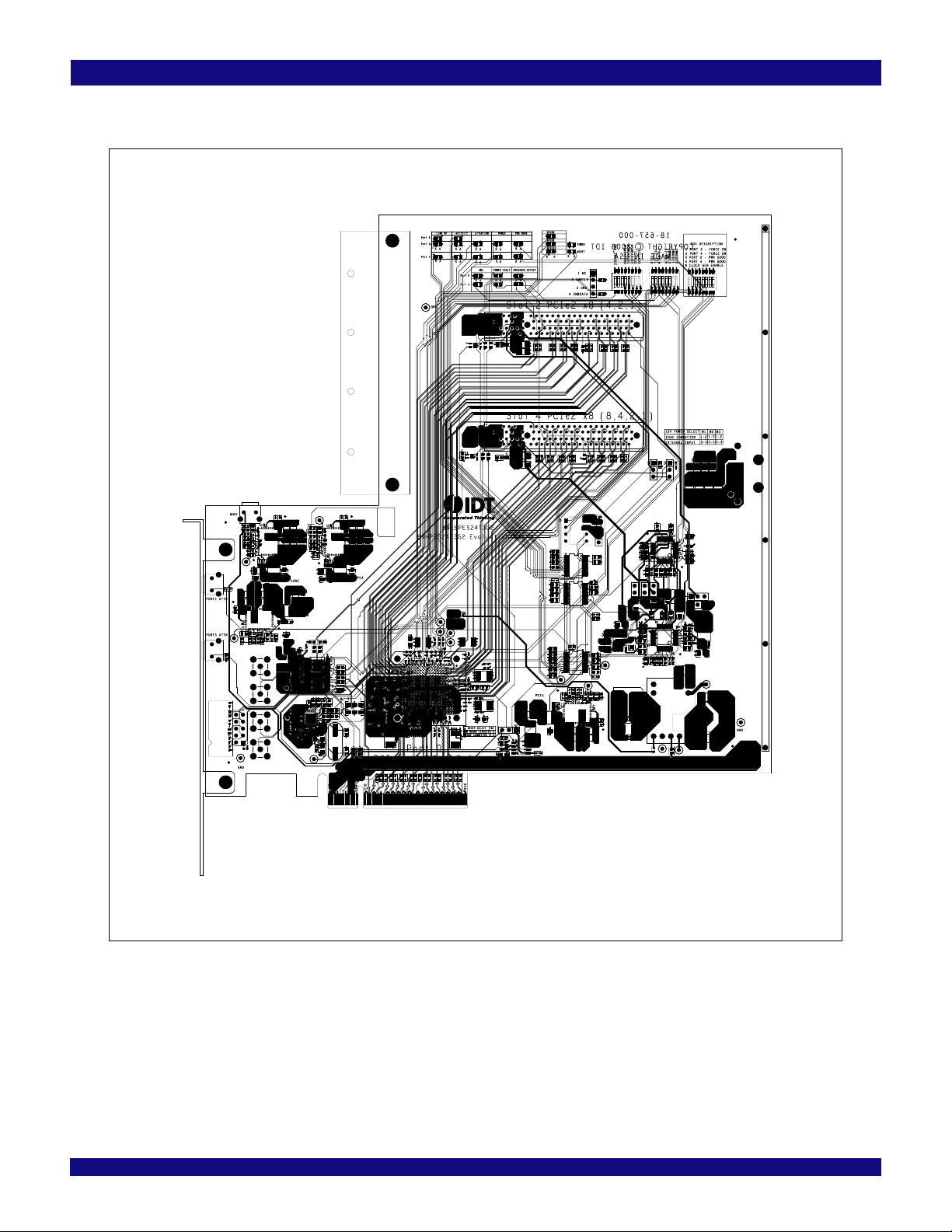
EB24T3G2 Board Figure
Slot 2
Slot 4
S6
S7
S8
Table of contents
Other IDT Motherboard manuals

IDT
IDT 89EBPES48H12 User manual

IDT
IDT 82P33731 User manual

IDT
IDT VersaClock 5 User manual

IDT
IDT 9ZXL1951D User manual

IDT
IDT VersaClock 6 5P49V69 Series User manual

IDT
IDT Tsi381 User manual

IDT
IDT Tsi620 User manual

IDT
IDT EB-LOGAN-23 User manual

IDT
IDT 8T49N240 User manual

IDT
IDT EVK-UFT285-6-7 User manual

IDT
IDT EB8T5A Eval Board User manual

IDT
IDT ADC1410S Series User manual

IDT
IDT ZMID520 Series User manual

IDT
IDT EB4T4 Eval Board User manual

IDT
IDT 82P33714 User manual

IDT
IDT ZMOD4510-EVK User manual

IDT
IDT P9221-R-EVK User manual

IDT
IDT ZSSC41 Series User manual

IDT
IDT ZSSC4151 User manual

IDT
IDT ZWIR4532 User manual


