2©2018 Integrated Device Technology, Inc. May 17, 2018
9FGV1006 PhiClock™ PCIe Evaluation Board User Guide
Board Power Supply
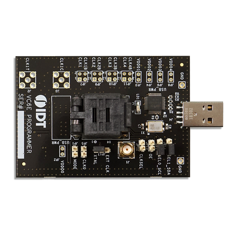
The evaluation board uses jumpers E1–E4 to set the power supply voltages for various VDD pins. The 4-way jumpers can select 3
different voltages from regulators that use power from the USB port. Selection #2 is the jack for connecting a bench power supply.
E1: Power supply for the REF outputs. The E1 voltage also determines the LVCMOS output levels of the REF0 and REF1 outputs.
E2: Power supply for the OUT0 output driver.
E3: Power supply for the OUT1 output driver.
E4: Power supply for the analog (VDDA) and digital (VDDD) core VDD pins.
See the 9FGV1006 PCIe Evaluation Board Schematics (Figure 4–Figure 7) for detailed information.
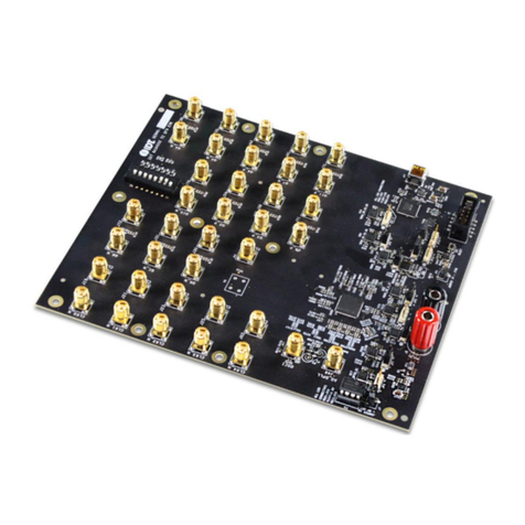
Table 1. Evaluation Board Pins and Functions
Label Number Name On-board Connector Label Function
1I
2C interface Connector J2 Alternative I2C interface connector for Aardvark.
IDT Timing Commander can also use Aardvark.
2 USB Connector J6
Connect this USB to your PC to run IDT Timing
Commander.
The board can be powered from the USB port.
3 Output Power Supply Jack J3 Connect to 1.8V, 2.5V or 3.3V for the output voltage of
the device.
4 Core Power Supply Jack J4 Connect to 1.8V, 2.5V or 3.3V for the core voltage of the
device.
5 Ground Jack J5 Connect to ground of power supply.
6 Differential Output 1 S3 & S4
This can be a differential pair, or two single-ended
outputs.
Available logic types: LVCMOS, LVDS and LP-HCSL.
7 Differential Output 2 S7 & S10
This can be a differential pair, or two single-ended
outputs.
Available logic types: LVCMOS, LVDS and LP-HCSL.
8Power Supply Voltage
Selector E1, E2, E3
VDD_REFP1, VDDO_0, VDDO_1, four-way headers
used to select a power supply voltage. Connect the
center pin to one of the 4 surrounding pins to select a
voltage or a source.
9Power Supply Voltage
Selector E4
VDDA0, four-way headers used to select a power supply
voltage. Connect the center pin to one of the 4
surrounding pins to select a voltage or a source.
10 Reference Output 0 S1 Reference or buffered output from the crystal.
11 Sel_I2C# JP3
I2C bus enable access registers.
OTP bank CFG0 used to initialize RAM configuration
registers.
12 SCL, SDA / SEL0, SEL1 JP1, JP2 OTP bank CFG used to initialize RAM configuration
registers.
