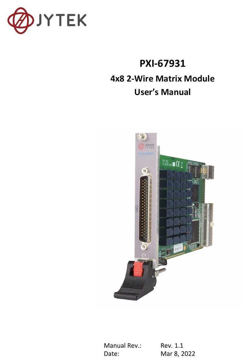
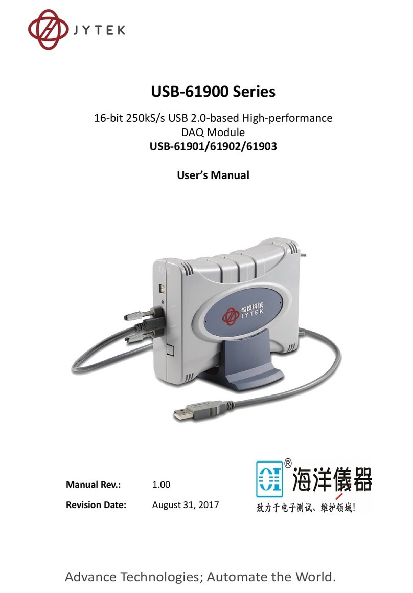
JYTEK USB-61210 User manual

Advance Technologies; Automate the World.
Manual Rev.: 1.00
Revision Date: July 31, 2017
USB-61210
4-CH 16-Bit 2MS/s Simultaneous-Sampling USB DAQ
Module
User’s Manual

ii

Preface iii
Preface
Copyright
This document contains proprietary information protected by copyright.
All rights are reserved. No part of this manual may be reproduced by
any mechanical, electronic, or other means in any form without prior
written permission of the manufacturer. All specifications are subject to
change without further notice.
Disclaimer
The information in this document is subject to change without prior
notice in order to improve reliability, design, and function and does not
represent a commitment on the part of the manufacturer.
In no event will the manufacturer be liable for direct, indirect, special,
incidental, or consequential damages arising out of the use or inability
to use the product or documentation, even if advised of the possibility
of such damages.
Environmental Responsibility
JYTEK is committed to fulfill its social responsibility to global environ-
mental preservation through compliance with the European Union's
Restriction of Hazardous Substances (RoHS) directive and Waste Electri-
cal and Electronic Equipment (WEEE) directive. Environmental protec-
tion is a top priority for JYTEK. We have enforced measures to ensure
that our products, manufacturing processes, components, and raw
materials have as liLVTTLe impact on the environment as possible.
When products are at their end of life, our customers are encouraged to
dispose of them in accordance with the product disposal and/or recov-
ery programs prescribed by their nation or company.
Trademarks
Product names mentioned herein are used for identification purposes
only and may be trademarks and/or registered trademarks of their
respective companies.

iv Preface
Conventions
Take note of the following conventions used throughout this manual to
make sure that users perform certain tasks and instructions properly.
NOTE:
NOTE:
Additional information, aids, and tips that help users perform tasks.
CAUTION:
Information to prevent minor physical injury, component damage,
data loss, and/or program corruption when trying to complete a
task.
WARNING:
Information to prevent serious physical injury, component damage,
data loss, and/or program corruption when trying to complete a spe-
cific task.

Table of Contents v
Table of Contents
Preface .......................................................................................... iii
Table of Contents............................................................................ v
List of Figures................................................................................ vii
List of Tables .................................................................................. ix
1 Introduction.............................................................................. 1
1.1 Overview........................................................................................ 1
1.2 Features ......................................................................................... 1
1.3 Applications ................................................................................... 1
1.4 Specifications ................................................................................. 2
1.4.1 General Specifications .........................................................2
1.4.2 Analog Input ........................................................................3
1.5 Schematics ..................................................................................... 4
1.5.1 Module ................................................................................4
1.5.2 Module Stand ......................................................................7
1.6 Connector Pin Assignment........................................................... 11
1.6.1 Connector Signal Description ............................................11
1.7 Analog Input Signal Connection................................................... 12
1.8 Software Support......................................................................... 14
1.9 Driver Support for Windows........................................................ 14
1.10 Utilities for Windows ................................................................... 14
2 Getting Started ....................................................................... 15
2.1 Unpacking Checklist..................................................................... 15
2.2 Attaching the Module Stand........................................................ 15
2.3 Rail Mounting .............................................................................. 16
2.4 Wall Mounting ............................................................................. 17
2.5 Installing the USB-61210 Module ................................................ 18

vi Table of Contents
2.5.1 Connecting the USB-61210 Module.................................. 18
2.5.2 Device ID ........................................................................... 19
2.5.3 Hardware Configuration.................................................... 20
3 Operation & Calibration........................................................... 21
3.1 Operation .................................................................................... 21
3.1.1 Signal Function .................................................................. 21
3.1.2 A/D Conversion ................................................................. 22
3.1.3 Trigger Sources.................................................................. 25
3.1.4 Trigger Modes ................................................................... 27
3.1.5 Programmable Function I/O.............................................. 31
3.1.6 Basic Timer/Counter Function .......................................... 32
3.1.7 General Purpose Timer/Counter Modes........................... 33
3.1.8 Isolation............................................................................. 39
3.2 Calibration ................................................................................... 39
3.2.1 Loading Calibration Constants .......................................... 39
3.2.2 Auto-Calibration................................................................ 40
3.2.3 Saving Calibration Constants............................................. 40
Important Safety Instructions ....................................................... 41
Warranty Policy ............................................................................ 43
Getting Service ............................................................................. 45

List of Figures vii
List of Figures
Figure 1-1: USB-61210 Module Rear View ............................................4
Figure 1-2: USB-61210 Module Side View .............................................5
Figure 1-3: USB-61210 Module Front View ...........................................6
Figure 1-4: Module, Stand, Connector, and USB Cable .........................7
Figure 1-5: Module, Stand, & Wall Mount Kit Side View (w/ connections)
8
Figure 1-6: Module in Stand Front View................................................8
Figure 1-7: Module Stand Top View ......................................................9
Figure 1-8: Module Stand Side Cutaway View.....................................10
Figure 1-9: Module Stand Front View..................................................10
Figure 1-10: GRND-Referenced Source w/ DIFF Input...........................13
Figure 1-11: Floating Source w/ DIFF Input ...........................................13
Figure 2-1: Rail Mount Kit....................................................................16
Figure 2-2: Module Pre-Rail Mounting ................................................16
Figure 2-3: Module Rail-Mounted .......................................................17
Figure 2-4: Wall Mount Holes..............................................................17
Figure 2-5: Module with Wall Mount Apparatus.................................18
Figure 2-6: USB-61210 module in Windows Device Manager.............19
Figure 2-7: Device ID Selection Control ...............................................20
Figure 3-1: Carrier Board Functional Block Diagram ...........................21
Figure 3-2: Daughter Board Functional Block Diagram .......................22
Figure 3-3: Analog Input ......................................................................23
Figure 3-4: Configuring Different Sampling Rates ...............................25
Figure 3-5: Below-Low Analog Triggering............................................26
Figure 3-6: Above-High Analog Triggering...........................................27
Figure 3-7: Digital Triggering ...............................................................27
Figure 3-8: Post Trigger without Retriggering .....................................28
Figure 3-9: Delayed Trigger..................................................................28
Figure 3-10: Middle Trigger ...................................................................29
Figure 3-11: Pre-Trigger.........................................................................29
Figure 3-12: Post Trigger with Retriggering ...........................................30
Figure 3-13: Gated Trigger.....................................................................30
Figure 3-14: Mode 1-Simple Gated-Event Calculation ..........................33
Figure 3-15: Mode 2-Single Period Measurement ................................34
Figure 3-16: Mode 3-Single Pulse-Width Measurement .......................35
Figure 3-17: Mode 4-Single-Gated Pulse ...............................................35
Figure 3-18: Mode 5-Single-Triggered Pulse..........................................36
Figure 3-19: Mode 6-Re-Triggered Single Pulse.....................................36
viii List of Figures
Figure 3-20: Mode 7-Single-Triggered Continuous Pulse...................... 37
Figure 3-21: Mode 8-Continuous Gated Pulse ...................................... 37
Figure 3-22: Mode 9-Edge Separation Measurement........................... 38
Figure 3-23: Mode 10-PWM Output Following Trigger......................... 38
Figure 3-24: Mode 10-PWM Output Following GATE Control .............. 38
Figure 3-25: Isolation............................................................................. 39

List of Tables ix
List of Tables
Table 1-1: USB-61210 Pin Assignment .....................................................11
Table 1-2: CN1/CN2 I/O Signal Description..............................................12
Table 3-1: Bipolar Analog Input Range and Output Digital Code.............23
Table 3-2: Pin Definition of LVTTL Digital I/O...........................................31
Table 3-3: Timer/Counter Pin Definition..................................................32

x List of Tables
This page intentionally left blank.

Introduction 1
1 Introduction
1.1 Overview
The USB-61210 is a 16-bit high-speed USB 2.0-based DAQ module
equipped with 4 analog input channels providing simultaneous sampling
at up to 2MS/s per channel. The USB-61210 delivers high accuracy and
excellent dynamic performance at maximum sampling rates and fea-
tures flexible trigger function. In addition, onboard 256MS FIFO ensures
no data loss during acquisition even with heavy loading on CPU or sys-
tem.
The USB-61210 is USB bus powered and equipped with removable
screw-down terminals for easy device connectivity, and the included
multi-functional stand can be used for desktop, rail, or wall mounting.
Suitable for high-speed data acquisition, laboratory and medical
research, the USB-61210 provides a reliable measurement solution at
an affordable price.
1.2 Features
Hi-Speed USB 2.0
USB bus power
4-CH simultaneous-sampling analog input, up to 2MS/s per chan-
nel
Analog and digital triggering
500VDC bus isolation
Removable screw terminal
Lockable USB cable for secure connectivity
Ready-to-use testing application (U-Test) included
1.3 Applications
Automotive testing
High-speed data acquisition
Laboratory research
Medical
I/O control
1.4 Specifications

2 Introduction
1.4.1 General Specifications
Digital I/O Specifications
Number of channels 8-CH programmable function digital input (DI)
4-CH programmable function digital output (DO)
Compatibility LVTTL (single-end) (supports 3.3V and 5 V DI but
3.3V DO)
Input voltage Logic low: VIL = 0.8 V max; IIL = 0.2 mA max.Logic
high: VIH = 2.0 V min.; IIH = 0.2 mA max.
Output voltage Logic low: VOL = 0.5 V max; IOL = 10 mA max.
Logic high: VOH = 2.6V min.; IIH = 10 mA max.
Supporting modes (only one can
be selected and function at the
same time, please see
Section 3.1.5: Programmable
Function I/O)
8-CH LVTTL DI and 4-CH LVTTL DO
2-CH 32-bit general-purpose timer/counters:
Clock source: internal or external
Max source frequency: internal: 80 MHz; exter-
nal: 10 MHz
2-CH PWM outputs”:
Duty cycle:1-99% (please see Section : Mode
10: PWM Output)
Modulation frequency: 20 MHz to 0.005Hz
Data transfers Programmed I/O
Physical, Power, and Operating Environment
Interface High speed USB 2.0 compatible, mini-USB connector
Dimensions 156 (L) x 114 (W) x 41 (H) mm (6.14 X 4.49 X 1.61 in.)
I/O Connector Two 20-pin removable screw-down terminals
Power requirement USB power (5 V @ 500 mA)
Operating environment Ambient temperature: 0 to 55C
Relative humidity: 10% to 90%, non-condensing
Storage environment Ambient temperature: -20 to 70 C
Relative humidity: 5% to 95%, non-condensing

Introduction 3
1.4.2 Analog Input
Resolution 16 bit
Channels 4 differential (simultaneous sampling)
Maximum sampling rate 2MS/s per channel
Programmable gain 1, 5
Input range (voltage) ± 10 V, ± 2 V
Offset error ± 1mV (gain=1)
± 0.2mV (gain=5)
Gain error Typical: ± 0.01% of FSR (gain=1 & 5)
Maximum: ± 0.02% of FSR (gain=1 & 5)
-3dB bandwidth 630kHz (gain=1)
600kHz (gain=5)
CMRR (fin=1 kHz) 80 dB (gain=1)
90 dB (gain=5)
SFDR (fin=10 kHz) 108 dB (gain=5)
SINAD (fin=10 kHz) 89 dB (gain=1 & 5)
THD (fin=10 kHz) 100 dB (gain=1 & 5)
SNR (fin=10 kHz) 89 dB (gain=1 & 5)
ENOB (fin=10 kHz) 14.3-Bit (gain=1 & 5)
Temperature Drift:
Gain Error 5 ppm/°C (gain=1 & 5)
Temperature Drift:
Offset Error
50µV/°C (gain=1)
20µV/°C(gain=5)
FIFO buffer 256 Msamples
Trigger sources Software, external digital, analog trigger
(from one analog input channel)
Trigger mode
Post trigger, pre-trigger, delay trigger, middle
trigger, gate trigger, post or delay trigger with
re-trigger
External A/D conversion
source Yes (from CONV)
Input coupling DC
Overvoltage protection Power on: ± 35 V
Power off: ± 15V
Input impedance 1 GΩ

4 Introduction
1.5 Schematics
1.5.1 Module
Figure 1-1: USB-61210 Module Rear View
Data transfer Programmed I/O, continuous (USB bulk
transfer mode)
NOTE:
NOTE:
All units are in millimeters (mm)

Introduction 5
Figure 1-2: USB-61210 Module Side View

6 Introduction
Figure 1-3: USB-61210 Module Front View

Introduction 7
1.5.2 Module Stand
The multi-function USB-61210 stand is compatible with desk, rail, or
wall mounting. To fix the module in the stand, slide the module body
into the stand until a click is heard. To remove the module from the
stand, twist the bottom of the stand in a back-and forth motion and sep-
arate from the module.
Figure 1-4: Module, Stand, Connector, and USB Cable

8 Introduction
Figure 1-5: Module, Stand, & Wall Mount Kit Side View (w/ connections)
Figure 1-6: Module in Stand Front View

Introduction 9
Figure 1-7: Module Stand Top View
20.4
20.4
B
26

10 Introduction
Figure 1-8: Module Stand Side Cutaway View
Figure 1-9: Module Stand Front View
5.89
1.5
6
3.4
100
Table of contents
Other JYTEK Control Unit manuals
Popular Control Unit manuals by other brands

Soundstream
Soundstream Tarantula SEC-TLA-RIDE quick start guide

Danfoss
Danfoss ASV-PV instructions

Tyco
Tyco DV-1 manual

Spirax Sarco
Spirax Sarco SafeBloc DBB3 Installation and maintenance instructions

Mitsubishi Electric
Mitsubishi Electric GT1030-HBD General description

TM Technologie
TM Technologie VIP TML installation instructions

Festo
Festo VSNZ-FT-T32C-M-F-P1-T Series Assembly instructions

White Rodgers
White Rodgers 50V64-743 installation instructions

AXIOMTEK
AXIOMTEK CEM312 Quick installation guide

Cameron
Cameron ORBIT GP-6 Installation operation & maintenance

Asus
Asus Aaeon NanoCOM-APL user manual

Eagle
Eagle 1403 installation manual