List of Figures xi
List of Figures
Figure 2-1: USB-61902 Module Rear View ..........................................11
Figure 2-2: USB-61902 Module Side View ...........................................12
Figure 2-3: USB-61902 Module Front View .........................................13
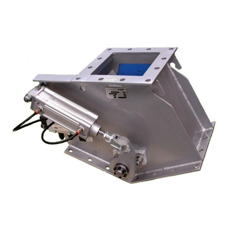
Figure 2-4: Module, Stand, Connector, and USB Cable .......................14
Figure 2-5: Module, Stand, & Wall Mount Kit Side View (w/ connections)
14
Figure 2-6: Module in Stand Front View..............................................15
Figure 2-7: Module Stand Top View ....................................................16
Figure 2-8: Module Stand Side Cutaway View.....................................17
Figure 2-9: Module Stand Front View..................................................17
Figure 2-10: Rail Mount Kit....................................................................18
Figure 2-11: Module Pre-Rail Mounting ................................................18
Figure 2-12: Module Rail-Mounted .......................................................19
Figure 2-13: Wall Mount Holes..............................................................20
Figure 2-14: Module with Wall Mount Apparatus.................................20
Figure 2-15: Floating source w/ RSE input connections ........................26
Figure 2-16: GRND-Referenced Sources w/ NRSE Inputs ......................27
Figure 2-17: GRND-Referenced Source w/ P-D Input ............................27
Figure 2-18: Floating Source w/ P-D Input.............................................28
Figure 2-19: Current Input .....................................................................29
Figure 3-1: USB-61900 module in Windows Device Manager.............32
Figure 3-2: Device ID Selection Control ...............................................32
Figure 4-1: Functional Block Diagram (USB-61902).............................36
Figure 4-2: Analog Input ......................................................................37
Figure 4-3: Analog Input Scan Timing ..................................................39
Figure 4-4: Below-Low Analog Triggering............................................42
Figure 4-5: Above-High Analog Triggering...........................................43
Figure 4-6: Digital Triggering ...............................................................43
Figure 4-7: Post Trigger without Retriggering .....................................44
Figure 4-8: Delayed Trigger..................................................................45
Figure 4-9: Post Trigger or Delay Trigger with Retriggering ................46
Figure 4-10: Gated Trigger.....................................................................47
Figure 4-11: Waveform Generation for Two Channel Update ..............49
Figure 4-12: FIFO Data In/Out Structure................................................49
Figure 4-13: Waveform Generation Hardware Timing ..........................51
Figure 4-14: Post-Trigger Waveform Generation ..................................52
Figure 4-15: Delayed-Trigger Waveform Generation ............................53
Figure 4-16: Post-Trigger or Delayed-Trigger with Retriggering............54
