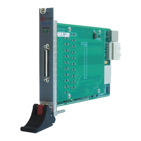
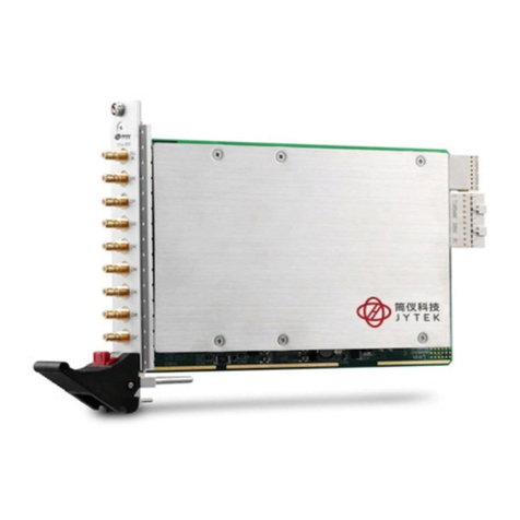
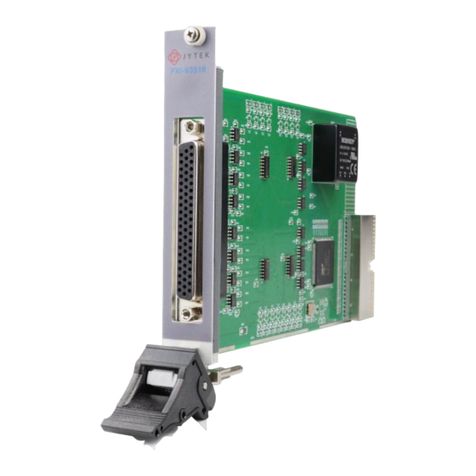
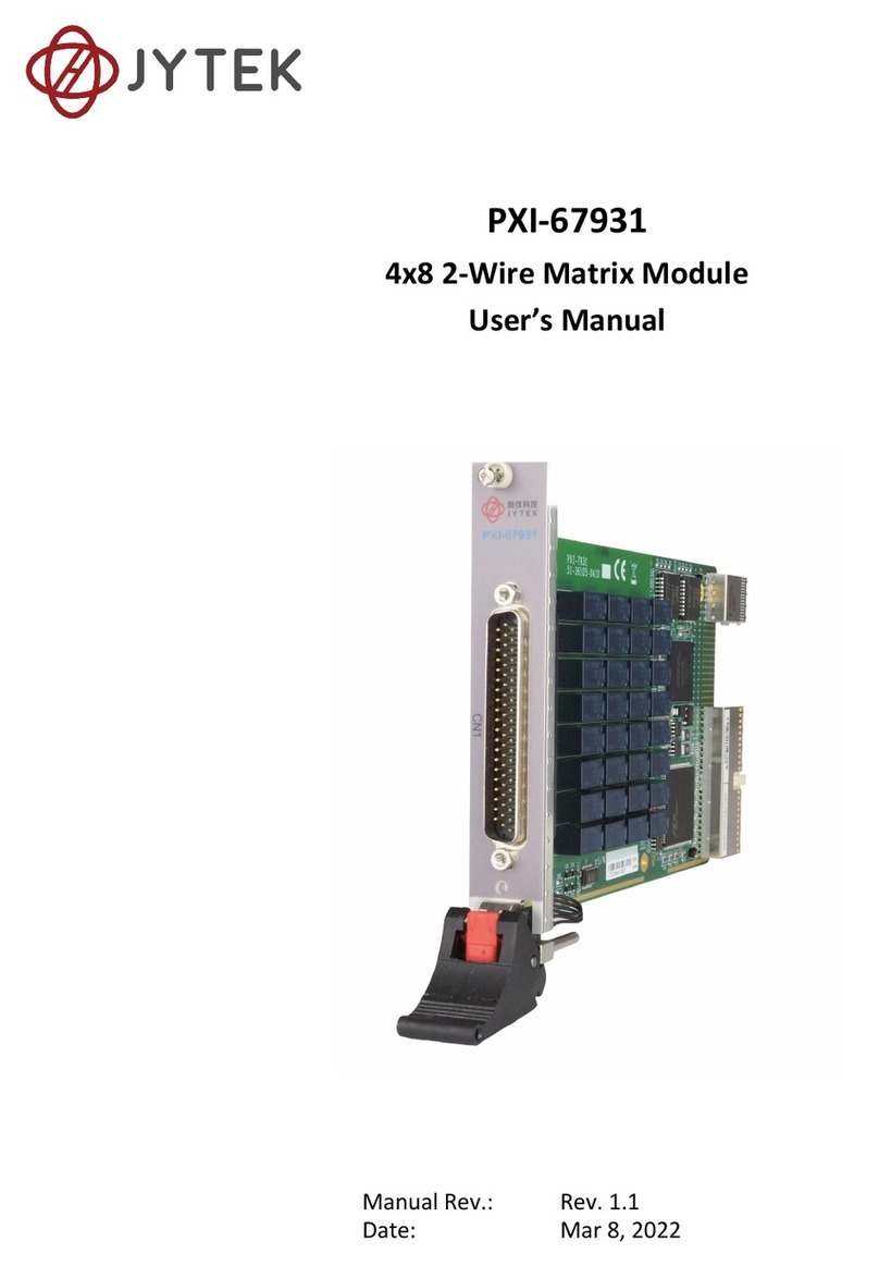
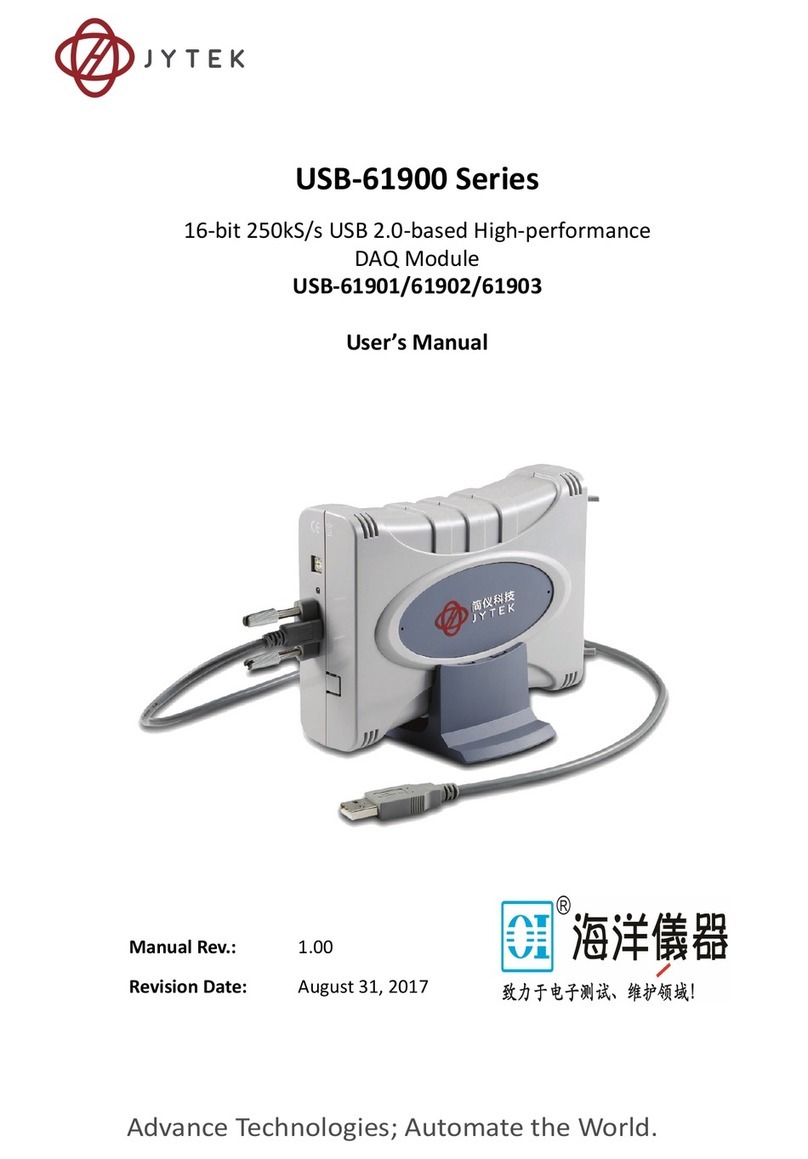
JYTEK PXI-67921 User manual

PXI-67921
24-ch,Multiplexer DPDT Relay Module
User’s Manual
Manual Rev.:
Date:
Rev. 1.0
February 8, 2020

Copyright © 2020 Shanghai Jianyi Technology Co., Ltd. All Rights Reserved.
Disclaimer
The information in this document is subject to change without prior notice in
order to improve reliability, design, and function and does not represent a
commitment on the part of the manufacturer.
In no event will the manufacturer be liable for direct, indirect, special,
incidental, or consequential damages arising out of the use or inability to use
the product or documentation, even if advised of the possibility of such
damages.
This document contains proprietary information protected by copyright. All
rights are reserved. No part of this manual may be reproduced by any
mechanical, electronic, or other means in any form without prior written
permission of the manufacturer.
Trademarks
NuDAQ™, NuIPC™, NuDAM™, NuPRO™are registered trademarks of
JYTEK Technology Inc. Other product names mentioned herein are used
for identification purposes only and may be trademarks and/or registered
trademarks of their respective companies.

Environmental Responsibility
JYTEK is committed to fulfill its social responsibility to
global environmental preservation through compliance
with the European Union's Restriction of Hazardous
Substances (RoHS) directive and Waste Electrical and
Electronic Equipment (WEEE) directive.
Environmental protection is a top priority for JYTEK. We
have enforced measures to ensure that our products,
manufacturing processes, components, and raw
materials have as little impact on the environment as
possible. When products are at their end of life, our
customers are encouraged to dispose of them in
accordance with the product disposal and/or recovery
programs prescribed by their nation or company.
Battery Labels (for products with battery)
废电池请回收
California Proposition 65 Warning
WARNING: This product can expose you to chemicals including
acrylamide, arsenic, benzene, cadmium, Tris(1,3-dichloro-2-
propyl)phosphate (TDCPP), 1,4-Dioxane, formaldehyde, lead,
DEHP, styrene, DINP, BBP, PVC, and vinyl materials, which are known to
the State of California to cause cancer, and acrylamide, benzene, cadmium,
lead, mercury, phthalates, toluene, DEHP, DIDP, DnHP, DBP, BBP, PVC,
and vinyl materials, which are known to the State of California to cause birth
defects or other reproductive harm. For more information go to
www.P65Warnings.ca.gov.

Table of Contents • i
Table of Contents
How to Use This Manual .............................................................. ii
Chapter 1 Introduction ..............................................................1
1.1 Features ............................................................................. 1
1.2 Applications ....................................................................... 2
1.3 Specifications ..................................................................... 2
1.4 Software Support ............................................................... 3
Chapter 2 Installation ................................................................5
2.1 Unpacking .......................................................................... 5
2.2 Mechanical Drawing ........................................................... 6
2.3 Installing the switch module into a PXI Platform ................ 6
Chapter 3 Signal Connection....................................................9
3.1 PXI-67921 Topology .......................................................... 9
3.2 PXI-67921 Pin Assignments & Descriptions .................... 10
3.3 TB-6221 Terminal Board .................................................. 13
2-wire MUX ........................................................................ 14
2-wire, 2-group MUX .......................................................... 15
2-wire, 4-group MUX .......................................................... 16
1-wire MUX ........................................................................ 17
4-wire MUX ........................................................................ 18
Chapter 4 Operation Theorem................................................19
4.1 Hardware Block Diagram ................................................. 19
4.2 Operation Mode ............................................................... 20
4.3 Handshaking .................................................................... 20
4.4 Trigger Bus ...................................................................... 24
4.5 Auxiliary Digital I/O........................................................... 26
4.6 Hot-Swap ......................................................................... 27
4.7 Emergency Shutdown ...................................................... 27
4.8 Watchdog Timer ............................................................... 28
Warranty Policy........................................................................31

ii • How to use this Manual
How to Use This Manual
This User Manual is designed to assist users in the installation of the JYTEK
PXI-67921, 24-ch Multiplexer DPDT Relay PXI Switch module.
Chapter 1 Introduction
Gives an outline and overview of JYTEK switch modules’
features, specifications, and applications.
Chapter 2 Installation
Describes how to install a switch module into a PXI chassis. For
software library and utilities installation, please refer to the
Software Users’ Guide.
Chapter 3 Signal Connection
Shows the pin assignments and terminal board connection of the
switch module.
Chapter 4 Operation Theorem
Describes function blocks on JYTEK switch modules and
operation instructions.

Introduction • 1
Introduction
JYTEK PXI-67921 is a relay multiplexer module which consists of 24 2-wire
relays (DPDT, 2 Form C). PXI-67921 provides 48x1 1-wire and 24x1 2-wire
and 12x1 4-wire configurations and typically connects one instrument, such
as a DMM, a digitizer or a signal source, with many points which need
measurement or excitation.
Relays of PXI-67921 can be updated by either direct-update mode or auto-
scan mode. The latter mode supports scanlist of 1k-sample for
deterministic scanning.
PXI trigger functions are fully supported and software programmable. The
multiple switch modules can be synchronized and triggered without additional
field wiring.
For safety critical applications, PXI-67921 module can switch to the preset
state by either asserting emergency shutdown manually, or watchdog timer
overflow event.
1.1
Features
•PXI specifications Rev. 2.0 compliant
•3U Eurocard form factor, CompactPCI compliant (PICMG 2.0 R3.0)
•PICMG 2.1 R2.0 CompactPCI Hot-Swap specifications compliant
•24-ch DPDT (2 Form C) non-latching relays
•Contact rating
•2A switching, 2A carrying
•220VDC, 125VAC
•125 operations per second
•1k-sample scanlist for deterministic scanning
•Provides handshaking signals to trigger external instruments
•Programmable emergency shutdown function and Watchdog timer for
safety critical applications
•Three auxiliary 3.3V/TTL digital inputs/outputs with 5V tolerance
•Supports PXI backplane triggers to synchronize multiple modules
•Fully software programmable
1

2 • Introduction
1.2
Applications
•Industrial ON/OFF control
•External high power relay driving and signal switching
•Laboratory automation
•Industrial automation
•Switch contact status sensing
•Limit switch monitoring
•Cooperating with other modules such as A/D and D/A peripherals to
implement a data acquisition and control system
1.3
Specifications
Relay Output
•Number of channels: 24
•Relay type: DPDT (2 Form C), non-latching
•Switching capacity:
•Max. switching current: 2A
•Max. switching voltage: 220VDC, 125VAC
•Max. switching power: 50VA, 60W
♦Max. carrying current: 2A
•Failure rate: 10µA
•Contact resistance: 100mΩ max.
•Relay set/reset time
•Operate time: 4ms max.
•Release time: 4ms max.
•Bounce time: 1ms max.
•Expected life:
•Mechanical life: 108 operations min.
•Electrical life: 5x10⁵ operations min. (1A @ 30VAC, resistive load)
•Data transfer: Programmed I/O
Auxiliary Digital I/O
•Numbers of channel: 3 inputs/outputs
•Compatibility: 3.3 V/TTL (5V tolerant)
•Data transfers: programmed I/O
Handshaking Signals
•Programmable polarity
•Logic level: 3.3 V/TTL (5V tolerant)
•Trigger In source: TRG_IN, PXI trigger bus, PXI star trigger in
•Scanner Advanced destination: S_ADV, PXI trigger bus

Introduction • 3
Safety functions
•Emergency shutdown
•Logic level: 3.3 V/TTL (5V tolerant)
•Active with logic low (for AUX2/SHDNn pin)
•Emergency shutdown sources: SHDNn, PXI star trigger input, PXI
trigger bus
•Watchdog timer
•Base clock available: 10MHz, fixed
•Counter width: 32-bit
•Watchdog Timer Overflow sources: Onboard 32-bit watchdog
timer, PXI star trigger input, PXI trigger bus
General Specifications
•I/O Connector: 62-pin D-sub male
•Operating temperature: 0 to 55°C
•Storage temperature: -20 to 70°C
•Humidity: 5 to 95% non-condensing
•Power requirements (when all relays are activated simultaneously)
+5V +3.3V
1A 400mA
•Dimensions (not including connectors)
•160 mm x 100 mm
1.4
Software Support
JYTEK's ADL-SWITCH driver package is for Microsoft Windows operating
systems, including Windows 98/ME/NT/2000/XP.
The driver package also provides utilities to test your switch module, as well as
programming samples and source codes in Microsoft Visual Basic and Visual
C/C++.
For other operating systems, please contact JYTEK for more information.

4 • Introduction
This page intentionally left blank.
Table of contents
Other JYTEK Control Unit manuals
Popular Control Unit manuals by other brands
Festo
Festo Compact Performance CP-FB6-E Brief description
Elo TouchSystems
Elo TouchSystems DMS-SA19P-EXTME Quick installation guide
JS Automation
JS Automation MPC3034A user manual
JAUDT
JAUDT SW GII 6406 Series Translation of the original operating instructions
Spektrum
Spektrum Air Module System manual

BOC Edwards
BOC Edwards Q Series instruction manual

KHADAS
KHADAS BT Magic quick start
Etherma
Etherma eNEXHO-IL Assembly and operating instructions
PMFoundations
PMFoundations Attenuverter Assembly guide

GEA
GEA VARIVENT Operating instruction
Walther Systemtechnik
Walther Systemtechnik VMS-05 Assembly instructions
Altronix
Altronix LINQ8PD Installation and programming manual

