manuals.online logo
Brands
  1. Home
  2. •
  3. Brands
  4. •
  5. Laird
  6. •
  7. Microcontroller
  8. •
  9. Laird BL654 User manual

Laird BL654 User manual

Version 1.1
www.lairdtech.com/bluetooth
2
© Copyright 2018 Laird. All Rights Reserved
Americas: +1-800-492-2320
Europe: +44-1628-858-940
Hong Kong: +852 2923 0610
Version
Date
Notes
Contributor(s)
Approver
1.0
27 June 2018
Initial version
Raj Khatri
Jonathan Kaye
1.1
13 Aug 2018
Updated DJ Jack Max voltage in Figure 1
Raj Khatri
Jonathan Kaye
www.lairdtech.com/bluetooth
3
© Copyright 2018 Laird. All Rights Reserved
Americas: +1-800-492-2320
Europe: +44-1628-858-940
Hong Kong: +852 2923 0610
1Overview .............................................................................................................................................................................4
2Laird BL654 Development Kit Part Numbers ......................................................................................................................4
3Package Contents................................................................................................................................................................4
4BL654 Development Kit –Main Development Board .........................................................................................................5
5Understanding the Development Board.............................................................................................................................7
5.1 BL654 Default Configuration and Jumper Settings....................................................................................................8
6Functional Blocks ................................................................................................................................................................9
6.1 Power Supply.............................................................................................................................................................9
6.2 Reset Button ............................................................................................................................................................14
6.3 SWD (JTAG) Interface...............................................................................................................................................15
6.4 Four-wire UART Serial Interface ..............................................................................................................................17
6.5 UART Mapping.........................................................................................................................................................17
6.6 nAutoRUN Pin and Operating Modes......................................................................................................................19
6.7 Virtual Serial Port Modes and Over-the-Air smartBASIC App Download ................................................................20
7Software............................................................................................................................................................................21
8Breakout Connector Pinouts.............................................................................................................................................22
8.1 SIO (Special Input/Output Sockets) Breakout Connectors ......................................................................................22
8.2 Additional Peripherals/Sensors ...............................................................................................................................27
8.2.1 Temperature Sensor ..........................................................................................................................................27
8.2.2 I2C Sensor (RTC Chip).........................................................................................................................................29
8.2.3 SPI Device EEPROM............................................................................................................................................30
8.2.4 Push Button and LED Connected to BL654 ........................................................................................................30
8.2.5 NFC External Antenna Connector and NFC Antenna RF Matching Circuit.........................................................32
8.2.6 Optional External Serial QSPI Flash IC................................................................................................................33
8.2.7 Optional 32.76 kHz Crystal.................................................................................................................................34
9Other Features..................................................................................................................................................................35
9.1 Current Consumption Measurement ......................................................................................................................35
10 Appendix ...........................................................................................................................................................................36
10.1 Coin Cell Insertion....................................................................................................................................................36
10.2 Coin Cell Removal ....................................................................................................................................................37
11 Additional Documentation................................................................................................................................................38
www.lairdtech.com/bluetooth
4
© Copyright 2018 Laird. All Rights Reserved
Americas: +1-800-492-2320
Europe: +44-1628-858-940
Hong Kong: +852 2923 0610
The Laird BL654 Development Kit provides a platform for rapid wireless connectivity prototyping, providing multiple options
for the development of Bluetooth Low Energy (BLE) plus Near Field Communication (NFC) applications.
The Laird BLE development kit is designed to support the rapid development of applications and software for the BL654
series of BLE modules featuring Laird’s innovative event driven programming language – smartBASIC or for use with the
Nordic SDK for C development. More information regarding this product series including a detailed module user’s guide and
smartBASIC user guides are available on Laird’s BL654 product page: http://www.lairdtech.com/products/bl654-ble-thread-
nfc-modules
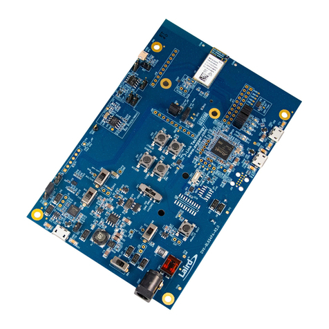
This document is applicable to the version of development board which has PCB silk screen text DVK-BL654-1.0.
Part Number
Product Description
455-00001
Development Kit for 451-00001 module –Integrated antenna
455-00002
Development Kit for the 451-00002 module –External antenna
Applicable to the following BL654 module part numbers:
Part Number
Product Description
451-00001
Bluetooth v5/802.15.4/NFC module –Integrated antenna
451-00002
Bluetooth v5 / 802.15.4 / NFC module –External antenna
All kits contain the following items:
Development Board
The development board has the required BL654 module soldered onto it and exposes all
available hardware interfaces.
Power Options
▪USB cable –Type A to micro type B. The cable also provides serial communications via
the FTDI USB –RS232 converter chip on the board.
▪DC barrel plug for connection to external power supply (5.5 VDC max)
▪3x AAA battery holder fitted on underside of development board
▪Coin-cell holder (powers module only) fitted on underside of development board
Two-pin jumpers
for pin headers (5)
Five jumpers for 2.54 mm pitch headers used on BL654 development board.
Fly leads (6)
Supplied (1 by 1 female to female jumper cable) to allow simple connection of any BL654
module pins (available on plated though holes or headers on J44, J47, J48, J41, J29, J1, J12, J1,
J5, J17, J21, J6 and J36).
External BLE
dipole antenna
Supplied with development kit part # 455-00002 only.
External antenna, 2 dBi, FlexPIFA (Laird part #001-0022) with integral RF coaxial cable with 100
mm length and IPEX-4 compatible RF connector.
External NFC
antenna
Supplied with development kit part # 455-00002 only
Laird NFC flexi-PCB antenna –Part # 0600-00061
Web link card
Provides links to additional information including the BL654 user guide, firmware, terminal
utilities, schematics, quick start guides, firmware release notes, and more.
Note: Sample smartBASIC applications are available to download from the Laird
https://github.com/LairdCP/BL654-Applications
www.lairdtech.com/bluetooth
5
© Copyright 2018 Laird. All Rights Reserved
Americas: +1-800-492-2320
Europe: +44-1628-858-940
Hong Kong: +852 2923 0610
This section describes the BL654 development board hardware. The BL654 development board is delivered with the BL654
series module loaded with integrated smartBASIC runtime engine firmware but no onboard smartBASIC; because of this it
starts up in AT command mode by default.
Applications in smartBASIC are simple and easy to develop for any BLE application. Sample smartBASIC applications scripts
are available to download from the Laird GitHub repository on the BL654 product page at
https://github.com/LairdCP/BL654-Applications. The development board also can be used with Nordic SDK.
The BL654 development board is a universal development tool that highlights the capabilities of the BL654 module. The
development kit is supplied in a default configuration which should be suitable for multiple experimentation options. It also
offers several header connectors that help isolate on-board sensors and UART from the BL654 module to create different
configurations. This allows you to test different operating scenarios.
The board allows the BL654 series module to physically connect to a PC via the supplied USB cable for development
purposes. The development board provides USB-to-Virtual COM port conversion through a FTDI chip –part number
FT232R. Any Windows PC (XP or later) should auto-install the necessary drivers; if your PC cannot locate the drivers, you
can download them from http://www.ftdichip.com/Drivers/VCP.htm
The BL654 development board has the following features:
▪BL654 series module soldered onto the development board
▪The following power supply options for powering the development board:
–USB (micro-USB, type B)
–External DC supply (3.5-5.5V)
–AAA batteries (three AAA battery holder fitted on underside of development board)
–USB (micro-USB, type B) –for direct use of BL654 USB interface as well
▪Powering the BL654 module in Normal Voltage mode (OPTION1) via selection switch (SW7). Regulated 3.3V or
Regulated 1.8V via selection switch (SW5).
▪Powering the BL654 module in High Voltage mode (OPTION2) via selection switch (SW7). Regulated 2.5V or 4.5V (from
3x AAA battery –4.5V) via selection switch (SW8). Option to inject external voltage anywhere between 3.5V to 5.5V
for the High Voltage mode (via J28).
▪Power supply option for coin-cell (CR2032) operation of the BL654 module only (not development board)
▪USB to UART bridge (FTDI chip)
▪BL654 UART can be interfaced to:
–USB1 (PC) using the USB-UART bridge (FTDI chip)
–External UART source (using IO break-out connectors J1 –No-Pop, Plated Through Holes) when the development
board is powered from a DC jack or AAA batteries) or from USB1 (when jumper fitted in J35).
–Atmel MCU by use of an analog switch to route the BL654 UART (for those customers working with Nordic SDK).
USB2 to Atmel to Atmel UART (via open solderbridges) to BL654 UART.
▪Current measuring options (BL654 module only):
–Pin header (Ammeter)
–10R Series resistor for differential measurement (oscilloscope)
▪IO break-out 2.54 mm pitch pin header connectors (plated through-holes) that bring out all interfaces of the BL654
module –UART, SPI, QSPI, I2C, SIO [DIO or AIN (ADCs)], PWM, FREQ, NFC –and allow for plugging in external
modules/sensors.
▪Pin headers jumpers that allow the on-board sensors (I2C sensor, LEDs) to be disconnected from BL654 module (by
removing jumpers).
▪Four on-board sensors:
–Analog output temperature sensor via header in series (no jumper by default)
www.lairdtech.com/bluetooth
6
© Copyright 2018 Laird. All Rights Reserved
Americas: +1-800-492-2320
Europe: +44-1628-858-940
Hong Kong: +852 2923 0610
–I2C device (RTC chip U16) via headers in series (no jumper by default)
–SPI device (EEPROM)
–QSPI device (Flash IC) via open solderbridges (by default)
▪Four buttons and four LEDs for user interaction
▪One reset button (via an analog switch)
▪NFC antenna connector on-board development board for use with supplied flexi-PCB NFC antenna
▪Optional external 32.768 kHz crystal oscillator and associated load capacitors. Not required for operation of the BL654;
is disconnected by open solder bridges by default.
▪Optional external serial (QSPI) flash IC. Not required for operation of the BL654; is disconnected by open solder
bridges by default.
▪Access to BL654 JTAG –also known as Serial Wire Debug (SWD)
▪On-board SWD (JTAG) programmer circuitry (USB2 to BL654 module SWD interface)
▪smartBASIC runtime engine FW upgrade capability:
–Via UART (using the FTDI USB1-UART)
–Via SWD (USB2 to BL654 SWD) using on-board JTAG programmer circuitry on the BL654 Development Kit
▪smartBASIC application upgrade capability:
–Via UART (using the FTDI USB-UART)
–Via OTA (Over-the-Air)
www.lairdtech.com/bluetooth
7
© Copyright 2018 Laird. All Rights Reserved
Americas: +1-800-492-2320
Europe: +44-1628-858-940
Hong Kong: +852 2923 0610
Figure 1: Dev board contents and locations
Figure 2: Development board 455-00001 (fitted with 451-00001 BLE module with integrated antenna)
SW7 select Normal
(VDD) or High
(VDD_HV) operation
SW8 Select
between 2.5V or
3xAAA(4.5V)
On-board SWD
interface and
programmer
circuitry
I2C device
U16
SPI EEPROM
device
J41 PTH
J47 PTH
J29 PTH
4 Buttons
USB1
NFC Antenna
Connector CON2
USB2
connector
USB-SWD
interface
DC Jack
5.5V DC
max input
CON1
USB3 connector
BL654 nRF USB
device
F USB I/F
Optional Serial
QSPI flash
J48 PTH
FTDI-FT232R
DC/USB
Power Source
Switch
SW4
Header J12
for nAutoRUN
J35
J1 Header Plated
Through Holes
(PTH) for UART
Temperature
Sensor
TP14 GND
Hook
LED2 LED1 LED3 LED 4
J37 J26 J45 J39
J5 (VSP)
Optional
32.768 kHz
Crystal
SW3 nReset
/BOOT Button
J7 (VDD)
Current
Measurement
J9 (VDD_HV)
www.lairdtech.com/bluetooth
8
© Copyright 2018 Laird. All Rights Reserved
Americas: +1-800-492-2320
Europe: +44-1628-858-940
Hong Kong: +852 2923 0610
Important! To ensure correct out-of-the-box configuration, the BL654 development board switches and jumpers must
be configured as shown in Figure 3.
Figure 3: Correct BL654 development board 455-00001 or 455-00002 jumper and switch settings (image for 455-00001)
SW7 middle position (default) for
Normal Voltage (VDD pin of BL654) operation
J12 Fit Jumper on Pins 2 & 1
SW5 Switch to 3v3
SW6 Switch to 3v3
SW11 position
right (default)
TP14 Black
Test Hook
SW4
Switch
to
USB1
www.lairdtech.com/bluetooth
9
© Copyright 2018 Laird. All Rights Reserved
Americas: +1-800-492-2320
Europe: +44-1628-858-940
Hong Kong: +852 2923 0610
Figure 4 shows the BL654 development board Power Supply block.
Figure 4: BL654 development Kit power supply
There are five options for powering the development board:
▪USB1 USB type micro-B connector –If it requires the FTDI USB1-UART (BL654) path
▪USB2 USB type micro-B connector –If it requires the Atmel USB2-SWD (BL654) path
▪USB3 USB type micro-B connector –If it requires the USB3 to USB (BL654) path
▪External DC supply (2.5V-5.5VV), into DC jack connector (CON1),
▪AAA batteries –Three AAA (4.5V) battery holder (J25) fitted on underside of development board
The external power sources are fed into selection switch SW4 which allows a selection between either USB sources or the
DC jack/AAA.
www.lairdtech.com/bluetooth
10
© Copyright 2018 Laird. All Rights Reserved
Americas: +1-800-492-2320
Europe: +44-1628-858-940
Hong Kong: +852 2923 0610
All the external power sources listed above are buck-boost regulated to a fixed 5V on the development board.
The BL654 module has the following power supply pins:
▪VDD pin (operating range of 1.7V to 3.6V) –Used for Normal Voltage mode
▪VDD_HV pin (operating range of 2.5V to 5.5V) –Used for High Voltage mode
▪VBUS pin (operating range of 4.35V to 5.5V) –Used for BL654 USB mode
It can be powered in the following ways:
▪Normal Voltage mode operation
Option 1 –Normal voltage power supply mode entered when the external supply voltage is connected to both the
VDD and VDD_HV pins (so that VDD equals VDD_HV). Connect external supply within a 1.7V to 3.6V range to the
BL654 VDD and VDD_HV pins.
For Normal Voltage mode operation, the BL654 Development Board power supply section generates the following:
–Regulated 3.3V
–Regulated 1.8V
and then via selection switch SW5 (default is 3.3V position), you can select whether to use 3.3V or 1.8V.
▪High Voltage mode operation
Option 2 –High voltage mode power supply mode (using BL654 VDD_HV pin) entered when the external supply
voltage in ONLY connected to the VDD_HV pin and the VDD pin is not connected to any external voltage supply.
Connect external supply within a 2.5V to 5.5V range to the BL654 VDD_HV pin. Leave the BL654 VDD pin unconnected.
For High Voltage mode operation, the BL654 Development Board power supply section generates the following:
–Regulated 2.5V
–3 x AAA generated 4.5V (or inject external voltage into J28pin1 up to 5.5V)
and then via selection switch SW8 (default is 2.5V position), you can select whether to use 2.5V or 4.5V.
Option 3 –High voltage mode with voltage via USB3
–For either option, if you use the BL654 USB interface, the BL654 VBUS pin must be connected to an external
supply within the range of 4.35V to 5.5V.
The BL654 development board power supply section is designed to cater to the above. Follow the following steps:
1. Set SW7 –Select one of the following three positions:
▪High Voltage mode operation and BL654 USB (connect USB cable to USB3 connector) –Top position. Source
from USB3.
▪Normal Voltage mode operation –Middle position (default). Source from SW5.
▪High Voltage mode operation –Bottom position. Source from SW8.
2. Depending on chosen SW7 position, select one of the following three positions:
▪Plug in USB cable into USB3 –If SW7 is set to Top position.
▪SW5 (either 3.3V or 1.8V) –Default SW5 on 3.3V position. If SW7 set to Middle position.
▪SW8 (either 2.5V or 4.5V (3xAAA)) –Default SW8 on 2.5V position. If SW7 set to Bottom position.
Table 1 summarises the dev-board on-board power sources and switch positions.
www.lairdtech.com/bluetooth
11
© Copyright 2018 Laird. All Rights Reserved
Americas: +1-800-492-2320
Europe: +44-1628-858-940
Hong Kong: +852 2923 0610
Table 1: Dev board power sources and switch positions
Selection Switch SW7 positions (silk screen)
Source
Voltage Operating mode
Dev Board Power Supply Switch Positions
SW5
Selects between
1.8V or 3.3V
SW8
Selects
between
2.5V or 4.5V
(3xAAA)
Connect
USB cable
into
USB3
Present selected voltage to the BL654 pin
BL654 VDD pin
BL654 VDD_HV
pin
BL654
VBUS pin
SW7 Top position –
Silkscreen: USB3
(Source from USB3)
High Voltage Mode with
BL654 USB used (USB3)
Note 1:
USB3 voltage
USB3
voltage
SW7 Middle position –
Silkscreen: SW5 SW6
(Source from SW5, Note 2:
)
Normal Voltage Mode
Decided by SW5
(default SW5 on 3.3V position)
N/A
N/A
SW7 Bottom position –
Silkscreen: AAA (SW8)
(Source from SW8)
High Voltage Mode
Note 1
Decided by
SW8
(default SW8 on
2.5V position)
N/A
Power Source and Switch Location Notes:
Note 1: No voltage is presented to VDD pin, as in High voltage mode, the VDD pin becomes an output voltage pin. It can
be used to supply external circuitry from the VDD pin. Before any current can be taken from the BL654 VDD pin,
this feature must be enabled in the BL654. Additionally, the VDD output voltage is configurable from 1.8V to
3.3V with possible settings of 1.8V, 2.1V, 2.4V, 2.7V, 3.0V, and 3.3V. The default voltage is 1.8V.
Note 2: When SW6 is set to position “coin-cell,” then the voltage selected with SW5 (default position 3V3) does not get
presented to the BL654. The CR2032 coin cell (in J34) voltage is not regulated but is fed directly to the BL654
module supply pin. Switch SW6 selects between the regulated 3V3V/1V8 and coin cell. The coin cell powers only
the BL654 module directly (on the development board); this is power domain VDD_nRF_SW through R46 0R.
Note: The development board for BL654 has on-board circuitry to allow access to BL654 SWD interface (via USB
connector USB2). Use USB2 only to power the development board when BL654 SWD interface is needed. Refer
to SWD Interface. When USB2 is used, USB1 does not need to be used for DC power.
www.lairdtech.com/bluetooth
12
© Copyright 2018 Laird. All Rights Reserved
Americas: +1-800-492-2320
Europe: +44-1628-858-940
Hong Kong: +852 2923 0610
The development board power supply circuitry special feature is it resolves whether the BL654 VDD pin is an input supply
pin (in Normal Voltage mode) or becomes an output supply voltage pin (in High Voltage mode).
On the development board, the power circuity net names are as follows:
▪VCC_3V3 –Supplies regulated 3.3V power to the FTDI chip as well as temperature sensor (U1).
▪VSUPPLY –Supplies regulated 3.3V or 1.8V via selection switch SW5 to net VSUPPLY which is connected to input of
Load switch U21.
▪VCC_2V5_5V5 –Selection switch SW8 supplies either regulated 2.5V or 3x AAA battery voltage (4.5V) can be used for
when BL654 is powered in High Voltage mode (using the VDD_HV pin).
▪V5V –The main development board power supply’s buck-boosted output (that is 5V) supplies a discrete regulator
made up of Q3 and U19. U19 OpAmp drives Q3 to generate regulated voltage (that then is connected to input of load
switch U20) that tracks control signal VDD_nRF_SENSE.
▪VDD_VSRC_nRF –Supplies the FTDI chip IO and all other sensors and circuitry. VDD_VSRC_nRF is generated from load
switches U20 or U19.
▪VDD_nRF_SENSE –Used as control signal to drive control pin of load switches U20 and U19. The source of
VDD_nRF_SENSE is the BL654 VDD pin. When BL654 is powered in High Voltage mode (using the VDD_HV pin), the
BL654 VDD pin becomes an output.
▪VDD_nRF_SW –Selection switch SW6 supplies either VDD_SRC_nRF or coin-cell (J34). When the BL654 operated in
Normal Voltage mode (SW7 in middle position and voltage source is either 1.8V or 3.3V selected by SW5). Also
supplies the I2C RTC chip (U16). The use case for powering this is that the RTC chip can be configured so that, after the
pre-determined time, the RTC chip outputs (via RTC_ALARM pin) a transition level that can be used to wake up the
BL654 module up from deep sleep.
▪VDD_nRFp –Supplies the BL654 series module only. Current measuring block on the development board only
measures the current into power domain VDD_nRFp (that is current going into header J7 pin 1).
▪VDD_nRF –Supplies the BL654 series module only and is to the current that has come out of the current measuring
block on the development board on header connector J7 pin 2.
▪VDD_HVp –Supplies the BL654 series module only. Current measuring block on the development board only measures
the current into power domain VDD_nRFp (that is current going into header J9 pin1).
▪VDD_HV –Supplies the BL654 series module only and is to the current that has come out of the current measuring
block on the development board on header connector J9pin2.
▪VBUS_nRFp –This voltage from USB cable plugged into connector USB3, that is directly fed to BL654 VBUS pin (via 0R
resistor R50) on net VBUS_nRF.
TIP: If operating the development board at temperature of 75°C or above there is an issue related to Q2 (it starts turning
on) which results in VDD_VSRC_nRF supplying heading towards 0V or turning off. To overcome this issue 75°C or above
issue, bridge with solder the open-solderbridge SB24 which connects 1MOhms resistor to ground onto the gate of Q2.
The 1-MOhm resistor results in extra current consumption of (= VDD_nRF_SENSE/1Mohms) added to any current
measurements made when operating the BL654 module on devboard in High voltage mode (VDD_HV pin) ONLY which
is when SW7 in Top position or Bottom position (and in that case by default VDD_nRF_SENSE is 1.8V). Figure 5 shows
PCB location of SB24 and schematic showing SB24.
www.lairdtech.com/bluetooth
13
© Copyright 2018 Laird. All Rights Reserved
Americas: +1-800-492-2320
Europe: +44-1628-858-940
Hong Kong: +852 2923 0610
Figure 5: Schematic and PCB location of SB24
U19
Dual OP,10uA/amp
OUT1 1
INV IN1 2
Non-INV IN1 3
VCC- 4
Non-INV IN2
5INV IN2
6OUT2
7VCC+
8
R137
1M
U20
Load-Switch-IC,1A
VOUT
1
GND
2
CONTROL
3NC 4
VIN 5
VDD_nRF_SENSE
R52
0R
VDD_nRF_SENSE
V5V
Q2
DUAL-NCH,+20V,800mA
S1
1
G1
2
D2
3
D1 6
G2 5
S2 4
GND
VSUPPLY_EN
R61
1M
C18
0.1uF,16V
GND
GND
GND
GND
Q3
NPN,+45V,2.0A
GND
SB15NOPOP (Solderbridge_Open)
1
122
VSUPPLY U21
Load-Switch-IC,1A
VOUT 1
GND 2
CONTROL 3
NC
4VIN
5
VDD_VSRC_nRF
SB24
NOPOP (Solderbridge_Open)
11
2
2
www.lairdtech.com/bluetooth
14
© Copyright 2018 Laird. All Rights Reserved
Americas: +1-800-492-2320
Europe: +44-1628-858-940
Hong Kong: +852 2923 0610
The coin cell powers only the BL654 module directly via SW6 (on the development board –power domain VDD_nRF_SW)
and through R46 provides power to the I2C RTC chip (U16).
Refer to the Appendix for the correct method of coin cell insertion and removal.
The development board has a reset button (SW3) with the net name BOOT_RESET_BLE. The BOOT_RESET_BLE (is active
low when SW3 pushed down) is routed to the BL654 module nRESET_BLE pin via an analog switch U25. The placement of
the Reset button is shown in Figure 6.
Figure 6: Reset button placement
Figure 7: Reset button schematic and routing through analog switch and location diagram
By default, whether the analog switch (U25) control line (USB_DETECT) is low (USB2 cable not plugged in) or high (USB2
cable plugged in), the nReset button (SW3) is routed via the analog switch (U25) to BL654 nReset pin (nRESET_BLE).
C63
NOPOP (0.01uF,16V)
GND
NOPOP (PIN HEADER,2.54mm 1X2P)
J42
11
2
2
GND
R34
150R
Reset
SW3
TACT SW,SMD/180d
1
1
2
233
44
BOOT_RESET_BLE
GND
SB22
NOPOP (Solderbridge)
1
122
BOOT_RESET_BLE
IMCU_BOOT
R1140R
VDD_VSRC_nRF
U25
Dual DPDT,1.65V~4.45V
1B0
1
1B1
15
2B0
5
2B1
3
1A 16
2A 4
1S 2
3B0
9
3B1
7
4B0
13
4B1
11
3A 8
4A 12
2S 10
GND
6
VCC 14
nRESET_BLE
GND
USB_DETECT
GND
C79
0.1uF,16V
www.lairdtech.com/bluetooth
15
© Copyright 2018 Laird. All Rights Reserved
Americas: +1-800-492-2320
Europe: +44-1628-858-940
Hong Kong: +852 2923 0610
The development board has USB2 cable detection circuit that generates the USB_DETECT signal on its output, so if a USB
cable is plugged into connector USB2, then USB2 cable detection circuit generates a HIGH on USB_DETECT or LOW if USB2
cable is not plugged in.
Table 3 displays the routing of SW3 reset button via analog switch U25 to the BL654 reset pin (regardless of whether the
USB cable is plugged into USB2 or not).
Table 2: USB U4 USB-SWD to BL654 SWD signal routing connections
SW3 reset button
into Analog switch
U25 (net name)
USB cable plugged into USB2
(USB_DETECT HIGH)
No USB cable plugged into
USB2 (USB_DETECT LOW)
Comments
Route SW3 reset button to BL654
(U5) reset pin
via analog switch U25
Net name
Route SW3 reset button to
BL654 (U5) reset pin
via analog switch U25
BOOT_RESET_BLE
nRESET_BLE
nRESET_BLE
R114 0R resistor if removed allows
SW3 to be disconnected from BL654
reset pin when USB2 cable plugged in.
The development board provides access to the BL654 module two-wire SWD interface on JP1 via analog switch U24. This is
REQUIRED for customer use, since the BL654 module supports smartBASIC runtime engine firmware over JTAG (as well as
over UART).
Note: We recommend that you use JTAG (two-wire interface) to handle future BL654 module firmware upgrades. You
MUST wire out the JTAG (two-wire interface) on your host design (four lines should be wired out, namely SWDIO,
SWDCLK, GND, and VCC). Firmware upgrades can still be performed over the BL654 UART interface, but this is
slower (60 seconds using UART vs. 10 seconds when using JTAG) than using the BL654 JTAG (two-wire interface).
Upgrading smartBASIC runtime engine firmware or loading smartBASIC applications also can be done using the UART
interface.
For those customers (using Nordic SDK) that require access to BL654 SWD (JTAG) interface, the BL654 development board
(see Figure 1) has on-board circuitry to allow access to BL654 module SWD interface (via USB connector USB2).
Figure 9 shows the SWD on-board circuitry routing via analog switch U24
When the USB cable is plugged into connector USB2 (the USB cable detection output generates a HIGH for USB_DETECT and
USB_DETECTp when switch SW11 is in position 2-1 –the default) and Atmel MCU SWD (JTAG) signals are routed to the
BL654 SWD interface. This is required to connect the two-wire SWD (JTAG) interface from U14 to the BL654 SWD (JTAG)
interface.
When the USB cable is plugged into connector USB2 and the SW11 is in position 2-3 (Low), there is a LOW on U24 control
line USB_DETECTp and the Atmel MCU SWD (JTAG) signals are routed to connector JP1 (which is not populated).
GND
SWDIO_EXT
SWDCLK_EXT
JP1
NOPOP (PIN HEADER,1.27mm 2X5P)
1 2
3 4
5 6
7 8
910 nRESET_EXT
SWO_EXT
VDD_VSRC_nRF
www.lairdtech.com/bluetooth
16
© Copyright 2018 Laird. All Rights Reserved
Americas: +1-800-492-2320
Europe: +44-1628-858-940
Hong Kong: +852 2923 0610
Figure 8: SW11 on development board (showing default position)
Figure 9: USB2 to SWD onboard circuitry routing via analog switch (U24)
OB_SWDIO
C80
0.1uF,16V
GND
OB_SWDCLK
SB21
NOPOP (Solderbridge_Open)
11
2
2
USB_DETECTp
VDD_VSRC_nRF
USB_DETECTp Pins connect
High 1A-->1B1,
2A-->2B1,
3A-->3B1,
4A-->4B1
SWDIO_EXT
SWDIO_BLE
SIO_32_SWO_BLE
nRESET_EXT
R131
NOPOP (0R)
U24
Dual DPDT,1.65V~4.45V
1B0
1
1B1
15
2B0
5
2B1
3
1A 16
2A 4
1S 2
3B0
9
3B1
7
4B0
13
4B1
11
3A 8
4A 12
2S 10
GND
6
VCC 14
OB_RESET
SWDCLK_BLE
SWDCLK_EXT
OB_SWO
USB_DETECTp
SWO_EXT
nRESET_BLE
USB_DETECT
SW11 position2-1 High (Default USB2-BL654-SWD)
SW11
Slide SW,SMD/180d
11
22
33
4
45
5
66
77
8
8
9
9
GND
GND
USB_DETECTp
GND GND
R138
1M
Q4
N-PCH,¡Ó20V,0.8A/-0.56A
S1
1
G1
2
D2
3S2 4
G2 5
D1 6
R139
100KR140
15K
GND
VDD_VSRC_nRF
VDD_USB_MCU
USB_DETECT
GND
SWDIO_EXT
SWDCLK_EXT
JP1
NOPOP (PIN HEADER,1.27mm 2X5P)
1 2
3 4
5 6
7 8
910 nRESET_EXT
SWO_EXT
VDD_VSRC_nRF
www.lairdtech.com/bluetooth
17
© Copyright 2018 Laird. All Rights Reserved
Americas: +1-800-492-2320
Europe: +44-1628-858-940
Hong Kong: +852 2923 0610
Table 3 displays the four signals running from Atmel MCU U14 (SWD interface plus SIO_32 and nReset_BLE) to the BL654
module (SWD interface plus SIO_32 and nReset_BLE).
Table 3: USB U4 USB-SWD to BL654 SWD signal routing connections
U4 (Atmel MCU) Net
SWD Interface into
Analog switch U24
USB cable plugged into USB2
(USB_DETECTp HIGH)
No USB cable plugged into USB2
(USB_DETECTp LOW)
Comments
Route SWD Interface from Atmel
MCU (U4) to BL654 Module
Net Name
Route SWD Interface from Atmel MCU
(U4) to JP1
OB_SWDCLK
SWDCLK_BLE (pin 3)
SWDCLK_EXT (JP1 pin4)
OB_SWDIO
SWDIO_BLE (pin 1)
SWDIO_EXT (JP1 pin2)
OB_RESET
nRESET_BLE (pin 19)
via R131 0R (Not populated)
nRESET_EXT (JP1 pin10)
OB_SWO
SIO_32 (pin 7)
SWO_EXT (JP1 pin6)
via SB21 open solderbridge
SIO_32 is a trace output (called SWO, Serial Wire Output) and is not necessary for programming BL654 over the SWD
interface.
nReset_BLE is not necessary for programming BL654 over the SWD interface.
The development board provides access to the BL654 module four-wire UART interface (TX, RX, CTS, RTS) either through
USB (via UT10 FTDI USB-UART convertor chip) or through a breakout header connector J1.
Note: The BL654 module provides four-wire UART interface on the HW and the other four signals (DTR, DSR, DCD, RI),
which are low bandwidth signals, can be implemented in a smartBASIC application using any spare digital SIO
pins.
The UART connection on the BL654 series module and the FTDI IC are shown in Table 4. Figure 10 explains how the BL654
series module UART is mapped to the breakout header connector J1. These connections are listed in Table 4.
Table 4: SIO/UART connections
BL654 (U5) SIO
BL654 Default Function
FTDI IC UART
SIO_06 (U5 pin35)
UART_TX (output)
USB_RX
SIO_08 (U5 pin29)
UART_RX (input)
USB_TX
SIO_05 (U5 pin39)
UART_RTS (output)
USB_CTS
SIO_07 (U5 pin37)
UART_CTS (input)
USB_RTS
Note: Additionally, SIO_35 (the nAutoRUN input pin on the module) can be driven by the USB_DTR output pin of the
FTDI chip. This allows testing the $autorun$ application on boot without setting the autorun jumper on the
development board. nAutorun can be controlled directly from Laird’s UWTerminalX using the DTR tick box.
www.lairdtech.com/bluetooth
18
© Copyright 2018 Laird. All Rights Reserved
Americas: +1-800-492-2320
Europe: +44-1628-858-940
Hong Kong: +852 2923 0610
▪USB Connector: The development kit provides a USB Type Micro-B connector (USB1) which allows connection to any
USB host device. The connector optionally supplies power to the development kit and the USB signals are connected
to a USB-to-serial converter device (FT232R) when SW4 is set to the USB position.
▪USB –UART: The development kit is fitted with a (U10) FTDI FT232R USB-to-UART converter which provides USB-to-
Virtual COM port on any Windows PC (XP or later). Upon connection, Windows auto-installs the required drivers. For
more details and driver downloads, visit the following website: http://www.ftdichip.com/Products/FT232R.htm.
▪UART Interface Driven by USB FTDI Chip: In normal operation, the BL654 UART interface is driven by the FTDI FT232R
USB-to-UART converter.
▪UART Interface Driven by External UART Source: The BL654 module UART interface (TX, RX, CTS, RTS) is presented at
a 2.54 mm (0.1”) pitch header (J1). To allow the BL654 UART interface to be driven from the breakout header
connector (J1), the following must be configured:
–The development board must be powered from a DC jack (CON1) or AAA batteries (J25) and with switch SW4 in
DC position.
–The FTDI device must be held in reset. This is achieved automatically by removal of the USB cable (from
connector USB1), placing SW4 in the DC position or fitting a jumper on J27.
–Fit a jumper on J35 (to switch the Analog switch U15 and route BL654 UART to J1) when connecting an external
UART source (for example FTDI USB-UART TTL (3.3V) converter cable) using J1. This isolates the BL654 UART
from the on-board USB-UART FTDI device. By default, the jumper on J35 is not fitted, so by default BL654 UART
is routed to U10 FTDI FT232R USB –UART converter.
Note: The BL654 UART signal levels always need to match the supply voltage net VDD_VSRC_nRF, of the BL654.
Figure 10: USB to UART (via FTDI chip on devboard) interface via analog switch U15
J1 pinout is designed to be used with FTDI USB-UART TTL (3.3V) converter cables (found at
http://www.ftdichip.com/Products/Cables/USBTTLSerial.htm). One example is FTDI part TTL-232R-3V3.
IMCU_CTS
IMCU_RxD
C8
0.1uF,16V
GND
IMCU_RTS
IMCU_TxD
USB_CTS
Module_CTS
VDD_VSRC_nRF
R7
10K
R6 0R
R9 0R
R12 0R
R21 0R
USB_RX
R19
10K
PIN HEADER,2.54mm 1X2P
J35
1
122
USB_DETECT Pins connect
High 1A-->1B1,
2A-->2B1,
3A-->3B1,
4A-->4B1
Module_RX
GND
SIO_08
VDD_VSRC_nRF
SIO_05
SIO_06
SIO_07 VDD_VSRC_nRF
USB_TX
USB_RTS
VDD_VSRC_nRF
U15
Dual DPDT,1.65V~4.45V
1B0
1
1B1
15
2B0
5
2B1
3
1A 16
2A 4
1S 2
3B0
9
3B1
7
4B0
13
4B1
11
3A 8
4A 12
2S 10
GND
6
VCC 14
Module_RTS
Module_TX
R2
10K
GND
R3
10K
R10
10K R11
10K
USB-UART
bridge chip
FTDI
FT232RQ
BL654
module
UART
BL654 UART J35
routed to FTDI: No Jumper in J35 (default).
routed to Atmel: Fit Jumper in J35.
www.lairdtech.com/bluetooth
19
© Copyright 2018 Laird. All Rights Reserved
Americas: +1-800-492-2320
Europe: +44-1628-858-940
Hong Kong: +852 2923 0610
If the BL654 on the development board is powered from 1.8V supply, then you must use the 1.8V version of the FTDI USB-
UART cable. UART signal levels always need to match the supply voltage net VDD_nRF_SW of the BL654 development
board.
Figure 11: J1 wiring to match FTDI USB-UART cable (TTL-232R-3V3 cable)
Fit a jumper in J35 (to switch the Analog switch U15 and route BL654 UART to J1) when connecting an external FTDI USB-
UART TTL (3.3V) converter cable using J1.
Fitting a jumper in J35 also allows the BL654 UART to be routed to Atmel MCU UART (signal also on J19 and net names
beginning with IMCU_) via open solder bridges SB16 to SB19 shown in Figure 12. You must connect these bridges with
solder. This may be useful for those customers wanting to work with the Nordic SDK.
Figure 12: Open solder-bridges on the UART interface running from Atmel MCU (U4) to analog switch U15 (to BL654 ultimately)
On the development board, the USB_DTR output (FTDI chip U10) from the PC is wired to BL654 module pin SIO_35 (pin 5)
which is the nAutoRUN pin.
Note: smartBASIC runtime engine FW checks for the status of nAutoRUN during power-up or reset. The nAutoRUN pin
detects if the BL654 module should power up into Interactive/Development Mode (3.3 V) or Self-contained Run
mode (0V). The module enters Self-contained Run mode if the nAutoRUN pin is at 0V and an application called
$autorun$ exists in the module’s file system, then the smartBASIC runtime engine FW executes the smartBASIC
application script automatically; hence the name Self-contained Run mode.
SIO_06
R1
NOPOP (0R)
Module pin BL654 UART Data Flow
SIO_06 Module_TX Output
SIO_08 Module_RX Input
SIO_05 Module_RTS Output
SIO_07 Module_CTS Input
SIO_07
SIO_08
VDD_VSRC_nRF
SIO_05
FTDI (USB to TTL 232 Cable)
GND
USB_CTS
VCC
USB_TX
USB_RX
USB_RTS
GND
RTS
VCC
RX
TX
CTS
J1
NOPOP (PIN HEADER,2.54mm 1X6P)
1
1
2
2
3
3
4
4
5
5
6
6
GND
IMCU_RTS_A
IMCU_RxD_A
SB19NOPOP (Solderbridge_Open)
1
122IMCU_TxD_A
IMCU_RTS
IMCU_CTS
IMCU_TxD
IMCU_RxD
SB16NOPOP (Solderbridge_Open)
1
122IMCU_CTS_A
SB17NOPOP (Solderbridge_Open)
1
122
SB18NOPOP (Solderbridge_Open)
1
122
www.lairdtech.com/bluetooth
20
© Copyright 2018 Laird. All Rights Reserved
Americas: +1-800-492-2320
Europe: +44-1628-858-940
Hong Kong: +852 2923 0610
Tying nAutoRUN HIGH (to net name on devboard VDD_VSRC_nRF) inhibits the $autorun$ application from running. As an
alternative to using USB_DTR, the J12 three-pin header allows a jumper to be fitted to select between the two operating
modes.
Table 5: BL654 nAutoRUN header
nAutoRUN
Pin
BL654 Operating Mode (pin28, nAutoRUN Mode/SIO_35)
Interactive/
Development Mode
(SIO_35 set High
Externally)
Self-contained Run
Mode (nAutoRUN
mode)
(SIO_35 Low
Internally)
Circuit
J12
Jumper
Position
Develop
Jumper on J12 pins 2-1
nAutoRUN (default)
Jumper on J12 pins 2-3
BL654 has internal
pull-down enabled,
jumper in J12 in 2-3
can also be left off
The J12 header connector allows the USB_DTR signal from the FTDI chip to be disconnected from the BL654.
To connect the BL654 nAutoRUN pin SIO_35 (pin 5) to PC FTDI USB_DTR line via the J12 header connector, do the following:
▪Fit the jumper into the J12 (pin 2-1) header connector to allow the PC (using UwTerminal) to control nAutoRUN pin
(SIO_35).
To disconnect the BL654 nAutoRUN SIO_35 (pin 5) from the PC FTDI USB_DTR line, do the following:
▪Remove the jumper on header connector J12 pin 2-1. Then nAutoRUN can be controlled by inserting the jumper onto
J12 (pin 2-3) as shown in Table 5 (this is the default). The BL654 by default has pull-down enabled on the SIO_35
(nAutoRUN) pin, so the jumper into J12 (pin 2-3) is optional.
The Over-the-Air (OTA) feature makes it possible to download smartBASIC applications over the air to the BL654. To enable
this feature, SIO_02 must be pulled high externally.
On the development board, header connector J5-pin1 brings out the BL654 SIO_02; J5-pin 2 brings out VCC_nRF_SW. To
pull BL654 SIO_02 high (to net name VCC_nRF_SW on devboard), fit jumper into header J5.
Note: When SIO_02 is high, ensure that SIO_35 (nAutoRun) is NOT high at same time, otherwise you cannot load the
smartBASIC application script.
This section discusses Virtual Serial Port (VSP) Command mode through pulling SIO_02 high and nAutoRUN (SIO_35) low.
Refer to the documentation tab of the BL654 product page:
http://www.lairdtech.com/products/bl654-ble-thread-nfc-modules.
Figure 13 shows the difference between VSP Bridge to UART mode and VSP Command mode and how SIO_02 and
nAutoRUN (SIO_35) must be configured to select between these two modes.
R25
NOPOP (10K)
USB_DTR
GND
VDD_VSRC_nRF
PIN HEADER,2.54mm 1X3P
J12
11
22
3
3
n_Autorun /
module_DSR
Module_DSR
Develop: Jumper J12 pin2-1 (default)
nAUTORUN: Jumper J12 pin2-3
SIO_35

Other manuals for BL654

5

Other Laird Microcontroller manuals

Laird BTM410 User manual

Laird

Laird BTM410 User manual

Laird BT740 Series User manual

Laird

Laird BT740 Series User manual

Laird RM024 User manual

Laird

Laird RM024 User manual

Laird DVK-WLM400 User manual

Laird

Laird DVK-WLM400 User manual

Laird DVK-BT900-S Series Quick setup guide

Laird

Laird DVK-BT900-S Series Quick setup guide

Laird RAMP User manual

Laird

Laird RAMP User manual

Laird Pinnacle 100 User manual

Laird

Laird Pinnacle 100 User manual

Laird BL654PA User manual

Laird

Laird BL654PA User manual

Laird Vela IF820 User manual

Laird

Laird Vela IF820 User manual

Laird BL600 Series User manual

Laird

Laird BL600 Series User manual

Laird DVK-SU60-2230C User manual

Laird

Laird DVK-SU60-2230C User manual

Laird BT830 Quick setup guide

Laird

Laird BT830 Quick setup guide

Laird Sterling-EWB User manual

Laird

Laird Sterling-EWB User manual

Laird BL652 User manual

Laird

Laird BL652 User manual

Laird RAMP-AC RF User manual

Laird

Laird RAMP-AC RF User manual

Laird DVK-BTM46 Series User manual

Laird

Laird DVK-BTM46 Series User manual

Laird DVK-BT730-SA User manual

Laird

Laird DVK-BT730-SA User manual

Laird BT830 Quick setup guide

Laird

Laird BT830 Quick setup guide

Laird BTM510 User manual

Laird

Laird BTM510 User manual

Laird DVK-BL600-SA User manual

Laird

Laird DVK-BL600-SA User manual

Popular Microcontroller manuals by other brands

Cypress EZ-PD CY4502 Guide

Cypress

Cypress EZ-PD CY4502 Guide

Texas Instruments SimpleLink MSP432P4 Series Technical reference manual

Texas Instruments

Texas Instruments SimpleLink MSP432P4 Series Technical reference manual

Cypress CY3684 user guide

Cypress

Cypress CY3684 user guide

Atmel SAM HA1G16A Xplained Pro user guide

Atmel

Atmel SAM HA1G16A Xplained Pro user guide

RDC R8810LV user manual

RDC

RDC R8810LV user manual

Intel Arria 10 FPGA user guide

Intel

Intel Arria 10 FPGA user guide

Hitachi H8S/2633 F-ZTAT Hardware manual

Hitachi

Hitachi H8S/2633 F-ZTAT Hardware manual

Cypress MB96640 Series manual

Cypress

Cypress MB96640 Series manual

Intel 8XC196MC user manual

Intel

Intel 8XC196MC user manual

Parallax BS2p Plus Pack AppKit manual

Parallax

Parallax BS2p Plus Pack AppKit manual

Lunos 5/ZII installation manual

Lunos

Lunos 5/ZII installation manual

mangOH Green DV4 Developer's guide

mangOH

mangOH Green DV4 Developer's guide

Atmel AT40K Application note

Atmel

Atmel AT40K Application note

Cypress Semiconductor enCoRe II user guide

Cypress Semiconductor

Cypress Semiconductor enCoRe II user guide

Infineon XC800 AP08113 Application note

Infineon

Infineon XC800 AP08113 Application note

Cypress Semiconductor enCoRe CY7C604XX Specification sheet

Cypress Semiconductor

Cypress Semiconductor enCoRe CY7C604XX Specification sheet

Cypress EZ-USB FX3 CYUSB3KIT-003 quick start guide

Cypress

Cypress EZ-USB FX3 CYUSB3KIT-003 quick start guide

Dialog Semiconductor SmartBond DA14585 user manual

Dialog Semiconductor

Dialog Semiconductor SmartBond DA14585 user manual

manuals.online logo
manuals.online logoBrands
  • About & Mission
  • Contact us
  • Privacy Policy
  • Terms and Conditions

Copyright 2025 Manuals.Online. All Rights Reserved.