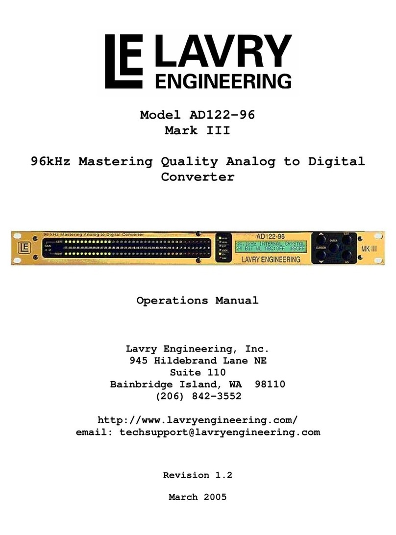
Lavry DA2002 User manual

Revision 1.5
http://lavryengineering.com
(206) 842-3552
Bainbridge Island, WA 98110
945 Hildebrand Lane NE Suite 110
Lavry Engineering, Inc.
Operations Manual
High Resolution Digital to Analog Converter
Model DA2002
ENGINEERING
LAVRY

2
DA2002 Operations Manual

3
www.lavryengineering.com
CrystalLock™ is a trademark of Lavry Engineering, Inc.
Acoustic Bit Correction® and Lavry Engineering® are registered trademarks of Lavry Engineering, Inc.
Copyright ©2002 by Lavry Engineering, Inc. All rights reserved.
INCIDENTAL DAMAGES, THE FOREGOING LIMITATION MAY NOT APPLY TO YOU.
NOT ALLOW THE EXCLUSION OR LIMITATION OF LIABILITY FOR CONSEQUENTIAL OR
ENGINEERING FOR THE APPLICABLE PRODUCT. BECAUSE SOME STATES/JURISDICTIONS DO
PURPOSE WHATSOEVER SHALL NOT EXCEED THE ORIGINAL COST PAID TO LAVRY
DAMAGES. ANY DAMAGES THAT LAVRY ENGINEERING IS REQUIRED TO PAY FOR ANY
EVEN IF LAVRY ENGINEERING HAS BEEN ADVISED OF THE POSSIBILITY OF SUCH LOSSES OR
FROM BREACH OF WARRANTY OR CONTRACT, NEGLIGENCE, OR ANY OTHER LEGAL THEORY,
PECUNIARY LOSS, ARISING OUT OF OR RELATING TO THE USE OF THE PRODUCT, OR ARISING
INTERRUPTION, LOSS OF BUSINESS INFORMATION, LOSS OF GOODWILL, COVER, OR OTHER
RECORDINGS, TAPES OR DISKS, DAMAGES FOR LOSS OF BUSINESS PROFITS, BUSINESS
EXEMPLARY LOSSES OR DAMAGES, INCLUDING, WITHOUT LIMITATION, DAMAGES TO
LIABLE FOR ANY INDIRECT, INCIDENTAL, CONSEQUENTIAL, PUNITIVE, SPECIAL OR
EXPRESSLY DISCLAIMS ANY IMPLIED INDEMNITIES. LAVRY ENGINEERING SHALL NOT BE
AND ALL SUCH WARRANTIES ARE HEREBY EXPRESSLY DISCLAIMED. LAVRY ENGINEERING
MERCHANTABILITY, FITNESS FOR A PARTICULAR PURPOSE, TITLE OR NONINFRINGEMENT,
EXPRESS OR IMPLIED, INCLUDING, WITHOUT LIMITATION, ANY WARRANTY OF
PERFORMANCE, COURSE OF DEALING, OR USAGE OF TRADE, MAKE ANY OTHER WARRANTIES,
LAVRY ENGINEERING DOES NOT, BY VIRTUE OF THIS AGREEMENT, OR BY ANY COURSE OF
LIMITS AND EXCLUSIONS
state/jurisdiction.
This limited warranty gives you specific legal rights. You may have others which vary from state/jurisdiction to
rental, service bureau, or similar businesses.
personnel. Lavry Engineering reserves the right to deny warranty service to products that have been used in
maintenance, alterations and modifications of the product, or service by an unauthorized service center or
damages which occur in shipment or failures resulting from accident, misuse, line power surges, mishandling,
provided. This warranty only covers failures due to defects in materials or workmanship and does not cover
coverage. A valid purchase receipt or other valid proof of purchase will be required before warranty service is
reseller of Lavry Engineering. Products that are purchased from unauthorized resellers do not have any warranty
This warranty is extended only to an original purchaser of the product from Lavry Engineering, or an authorized
number prior to shipment. No product will be accepted for warranty service without a pre-issued RMA number.
Lavry Engineering may exchange new or rebuilt parts for defective parts. Please call the factory for an RMA
workmanship.
Engineering will repair the product free of charge in the United States in the event of a defect in materials or
Subject to the conditions set forth below, for one year after the original purchase date of the product, Lavry
LIMITED WARRANTY
Operations Manual DA2002

4
Specifications............................................................................................11
Part III
Maintenance..............................................................................................10
Power and Fusing......................................................................................10
Output filter and drivers............................................................................10
Jitter removal...............................................................................................9
Timing and deglitcher .................................................................................9
Calibration...................................................................................................8
Oven control................................................................................................8
Theory of operation.....................................................................................8
Part II
CrystalLock™ and Wide lock.....................................................................7
Polarity inversion ........................................................................................7
Turn-On sequence.......................................................................................7
Analog Output Level ..................................................................................6
Analog Outputs............................................................................................6
Input signal connection ...............................................................................5
Input signal selection ..................................................................................5
Operating Instructions.................................................................................5
PART I
Introduction.................................................................................................4
Limited Warranty........................................................................................2
Table of Contents
DA2002 Operations Manual

5
• Supports New Hi-density I/O Standards from Sonic Solutions
• Professional and consumer inputs and outputs
• CrystalLock™ Digital Jitter removal
• Increased low level accuracy
• Automatic calibration
• Very low Total Harmonic Distortion + Noise
• Multi-bit architecture with 24 bits, non Sigma-Delta
• 96kHz, 88.2kHz, 48kHz and 44.1kHz conversion frequencies
Additional features:
signal reconstruction.
adjustments. The adjustments are done with sub pico-second resolution, to insure minimum interference with
measurement compares the average input frequency to the oscillator frequency and makes the appropriate
memory to the DAC disregarding any jitter in the input frequency. A proprietary fast-lock high-accuracy
and a short buffer memory for temporary storage of the incoming data. The DSP transfers the data from the
The DA2002eliminates jitterin the incoming data stream by use of a DSP controlled pullable crystal oscillator
transitions. A quad switch deglitcher circuit removes the unwanted transition glitch energy.
The DC offset provides superior low level detail by keeping low level signals away from the most significant bit
A large number of extra codes enable the addition of digital DC offset to the signal path without signal clipping.
extensive use of continuous automatic self-calibration.
critical components at constant temperature in a linearly controlled oven.Long term accuracy is achieved by
design improves the accuracy of the 10 most significant bits. Short-term accuracy is maintained by keeping the
The DA2002 provides many enhancements to the classical resistor weighting architecture. Atriple segmented
of the new standards (80-100KHz).
of the finest details. The DA2002 accommodates today's standard sample rates (40-50KHz) and the higher rates
linearity, small quantization steps, fast and accurate response and low noise performance enables reproduction
The DA2002 converts incoming digital inputs to 24 bit analog audio signals. The combination of excellent
Introduction
Operations Manual DA2002

6
SPDIF (consumer format) input to IEC INPUT.
AES/EBU input to the XLR connector designated as AES INPUT 2
AES/EBU input to the XLR connector designated as AES INPUT 1
The unit can be connected to one, two or three digital input connectors located on the rear panel:
Input signal connection
the input search mode, or visa versa. The mode selected is retained when power is removed.
Holding the INPUT SELECT button for more than one second switches between manual input selection and
will step through the inputs but will skip the inactive input connectors (where no signal is present).
Holding the INPUT SELECT button for more then a second makes the DA2002 go into search mode: the unit
button moves to the next input position.
The INPUT SELECT lamp indicators show the selected input signal. Pressing theINPUT SELECT push
Input signal selection
INPUT SELECT: Controls selection of digital inputs to the DAC.
POLARITY: Inverts the absolute polarity of the signal.
located on the front panel.
Operation of the Model DA2002 Digital to Analog Converterrequires the use of two push button switches
PART I: Operating Instructions
DA2002 Operations Manual

7
load, 2V R.M.S. into 600Ohms.
For Un-balanced XLR connection: The analog output level for a full-scale signal is 2.2V R.M.S. Into 100KOhm
load, 4.2V R.M.S. into 600Ohms.
For Balanced XLR connection: The analog output level for a full-scale signal is 4.5V R.M.S. Into 100KOhm
The analog output level at the IEC connectors for a full-scale signal is 2V R.M.S. into 100KOhm
Analog Output Levels
J10 jumper settings.
The LEFTOUTPUT and RIGHT OUTPUTIEC signals are always unbalanced and are not effected by J8 and
Pin 1 of the XLR connectors is connected to ground potential for proper cable shield connection.
For Unbalanced mode position the jumpers are set to 90 degrees with respect to the front panel.
The factory default setting is for Balanced outputs-- the jumpers are positioned parallel to the front panel.
J8 and J10 located behind the XLR analog output connectors inside the case.
Operation in unbalanced mode (signal at pin 2 and ground at pin 3) is possible by changing the internal jumpers
(signal between pin 2 and pin 3 of the XLR connectors).
The LEFT OUTPUT and RIGHT OUTPUTXLR signals are factory set to provide Balanced analog signals
Analog Outputs
Operations Manual DA2002

8
Note: changing between Crystall lock and normal lock requires a signal to be present at the unit input.
by blinking the appropriate status light periodically. This mode setting is retained when power is removed.
CrystalLock™, press and hold the POLARITY button again. The unit indicates wider lock (varispeed) mode
To normal (wider range) lock, press and hold thePOLARITY button for 1.5 seconds. To return to
interference with signal reconstruction.
appropriate adjustments. The adjustments are done with sub pico-second resolution, to insure minimum
accuracy measurement compares the average input frequency to the oscillator frequency and makes the
data from the memory to the DAC disregarding any jitter in the input frequency. A proprietary fast-lock high-
crystal oscillator and a short buffer memory for temporary storage of the incoming data. The DSP transfers the
The DA2002eliminates jitterin the incoming data stream by use CrystalLock™, a DSP controlled pullable
CrystalLock™ and Wide lock
Inverting while in balanced operation swaps pin 2 and pin 3 of the XLR connector.
Inverting while in unbalanced operation impacts signal polarity on pin 2 of the XLR connector.
Inverting while in unbalanced operation impacts signal polarity on the IEC center conductor.
a lit INVERT lamp.
The normal polarity is set to pin 3 hot. To invert, press thePOLARITY switch. Signal inversion is indicated by
Polarity inversion
found in other DACs.
that found in other DACs but the sound is not compromised. The spike due to power off is comparable to that
its output stage, thus disabling the drive capability during turn on. The DA2002 turn on spike may be higher then
with relay contacts. The unit deals with the turn on spike by incorporating very slow tracking power supplies for
proper operating conditions). The DA2002 contains no relays, in order to avoid signal degradation associated
Most DACs contains relays for the purpose of muting the output during turn on (allowing the DAC to settle to
indicated by the input select lamps if in auto select mode.
(44.1, 48, 88.2 or 96KHz). When all inputs are inactive, the unit steps through the input ports continuously as
The DA2002 figures out the incoming sample rate for the selected input and displays the incoming frequency
4. The unit finds the first active input and converts digital audio to analog sound.
minutes. During calibration, the unit blinks the two lower status lamps (88.2 and 96 light emitting diodes).
3. When set temperature is reached, the unit goes into self-calibration mode. The calibration time may take a few
blinks the two upper status lamps (44.1 and 48 light emitting diodes).
time depends on the initial temperature and may take up to 5 minutes for a cold unit. During warm-up, the unit
2. Warm-up: An internal oven heats up the temperature-sensitive devices to a set temperature. The warm-up
1. The unit goes into mute mode.
When applying AC power to the unit, the following sequence of events takes place:
Turn-On sequence
DA2002 Operations Manual

9
effective adjustment of a part in 5 million per calibration DAC step.
resistor, thus a full 10V swing on the calibration DAC can only pull a given node by +/-4mV, providing an
bit device to ensure monotonic performance. Each DAC is fed to its corresponding node through a large value
measured node. This is done via the calibration 14 bit DACs (see diagram). Each calibration DAC is used as a 13
comparator strobing cycle, the processor decides whether to increase or decrease the specific voltage of the
The strobing is repeated 4000 times for the sake of averaging out any error due to amplifier noise. At the end of a
comparator gain blocks in the simplified diagram). The processor strobes the comparator and reads its output.
greatly amplified and then fed to a strobing comparator (see multiplexers for calibration and error amplifier and
processor the required adjustments. The voltage difference between any given network node and the reference is
A sequence where each resistor is tapped (one at a time) for voltage comparison against a reference level tells the
Calibration
variations.
Keeping the resistors at constant temperature overcomes resistor dependency on environmental temperature
such as a home thermostat is undesirable because it produces turn on and turn off surges-- thus audible kicks.)
networks are kept at a constant temperature by a linearly controlled heating element. (A bang-bang controller,
subject to short term drift due to temperature variations and long term drift due to component aging. The resistor
The PCM DAC is constructed of custom made laser trimmed thin film resistor networks; yet any resistor is
Oven control
The simplified block diagram (figure 1) shows the basic building blocks.
Part II: Theory of operation
Operations Manual DA2002

10
the jitter content is random, much is due to coupling of the data itself into the receiver circuitry.
rejection of low frequency jitter content (typically hundreds of Hz of zero rejection bandwidth). While some of
signal. The need to keep enough bandwidth for locking to and tracking the incoming data translates to zero
incoming clock. The same circuits perform very poorly in the removal of low frequency jitter from the clock
Ordinary phase lock loops circuits (PLLs) do a reasonable job at removing high frequency jitter from the
Jitter removal
feeding the deglitcher circuit a precise jitter free on / off drive signal.
be somewhat sloppy, as long as the signals are well settled prior to turn on. Fighting the jitter wars means
deglitcher turn on and turn off are critical for good results. In fact switching during deglitcher blocking time can
timing point is all at the deglitcher circuit. Each sample value must exist over the same time period thus precise
The main reason for using DMOS transistors is their sub nanosecond switching capabilities. The jitter critical
resistance variations is neutralized by use of the strong feedback of the deglitcher amplifier.
technology thus providing extremely low resistance during the on state. The remaining problems due to on state
(switch two and four) are shorted to allow the signal path to the output. The deglither circuit utilizes DMOS
During the deglitcher on state, the shunt switches (switch one and three) are opened and the series switches
third switch. The remaining tiny energy is further blocked by the fourth opened series switch.
connected to the second switch that is in open state. Whatever comes through gets shunted to ground be the
The deglitcher utilizes four switches: the first switch shunt (shorts) the signal to ground. The remaining signal is
values should feed forward less than one microvolt. A single switch can not yield such blocking performance.
The blocking requirement is very demanding because a transition of many volts between two adjacent sample
the transitions from feeding forwards to the output filter.
output filter with minimum disturbance. The deglitcher off time settling requires the circuit to block as much of
critical time and no digital activity takes place anywhere near the analog circuits. The settled signals are fed to the
The deglitcher circuit is in off state about half a sample time, and on for the rest of the time. The on time is the
disappear, and for each new analog sample to accurately settle to its final value.
from feeding to the output for long enough time after each transition, thus allowing the glitches enough time to
and can not be removed by filtering. The purpose of the deglitcher circuit (see diagram) is to block the signal
Such switching causes unwanted glitch energy to come into play. The glitch energy is code and signal dependent
corresponding setting of analog switches and multiplexers to tap the appropriate voltage from the analog nodes.
The conversion from a digital sample value to an analog voltage consists of translating a digital code to a
Timing and deglitcher
minutes typically.
conditions (ovenized components). The remaining calibration at each subsequent power on takes less then 2
already, and each new calibration needs to deal only with component drift under the same given temperature
adjustments are initialized to the last settings. Therefore the initial tolerance of the components is pre calibrated
calibrated, the settings are stored in non volatile ram for future startup point of reference, thus all future
solution by design. Calibrating a DA2002 for the first time (at the factory) often exceeds 25 minutes. Once
nodes interaction exist during the adjustment process, the overall network is guaranteed to converge on a
nodes. The processor repeats the calibration cycle numerous times until all the nodes are set properly. Though
some misadjustment at all the other nodes). A single calibration cycle consists of reading and adjusting of all the
The calibration process takes a long time because the node adjustment is interactive (adjusting a node causes
DA2002 Operations Manual

11
fingerprints.
The front panel is gold plated (24 karat gold). Use a soft cloth (and plain water, if necessary) to clean
a long-term reliability standpoint.
maximum). The temperature rise is no cause for concern, but allowing for some airflow is always a benefit from
linear power supplies and discrete class A analog circuitry generates a significant amount of heat (25 watts
The Model DA2002 is an auto-calibrating converter requiring no periodic adjustments. The unit's reliance on
Maintenance
operation requires 115 volts AC.
Operation up to 240 volts is possible with no change in performance using the 220 volt setting. Optimal
accommodated. Two fuses are required.
operation requires 1/4 ampere 250 volt fast blow fuse. Both American and European size fuses can be
switchable on the back panel. 115 volts operation requires a 1/2 ampere 250 volt fast blow fuse; 220 volt
The Model DA2002 operates at 50 or 60 Hz, and has two line voltage selections, 115 volts and 220 volts,
Power and Fusing
side) may prove useful.
electrically noisy environment, a termination impedance of 600 Ohms (at the destination, not at the DA2002
loads. As always, for best results it is recommended to use high quality cables. When running a cable through an
The transistor based output drivers are short circuit protected and are capable of driving balanced 300 Ohm
incorporates a seven pole analog filter.
oversampling operation pauses an increased requirement for analog anti imaging filtering. The DA2002
further reduce sensitivity to jitter. The upsampling filter is calculated by the DSP. The tradeoff in favor of low
The DA2002 operates in low oversampling to allow for maximum settling time of the DAC circuits and to
Output filter and drivers
of D/A update rate.
requires pre storage of about 5 words of data for 1 second D/A stepping, or an 50 word memory for 10 seconds
fact, the data storage is very small and so is the delay. An "unrealistic" 100ppm per second input rate step
At first glance one may get concerned about the potential long delay due to storage of a lot of data samples. In
or becomes empty.
track, the long-term average drift is done just fast enough to make sure that the buffer memory does not overfill
data in a dedicated memory to guarantee that each clock cycle can find its data. Moving the clock slowly to
between the input and the too steady of a clock circuit. The DA2002 CrystalLock (TM) approach, stores enough
PLL will cause loss of lock because the slight variations in incoming data rate cause loss of correspondence
more) in a manner allowing it to track only very long term average drift. Using such an approach with ordinary
filter circuit). The oscillator frequency is change by tiny amounts (.1ppm) and not very often (15 seconds or
variations. The clock oscillator is controlled by a processor driven DAC (not an ordinary phase detector plus
crystal oscillator but the control signal for the crystal is freed from having to track down incoming clock
The DA2002 uses a non-standard approach for removing jitter. The deglitcher circuit is clocked by a pullable
Operations Manual DA2002

12
Input Voltage 115V 60Hz or 220V 50Hz, 20 Watts
Warm-up and initial calibration 10 minutes maximum, 3 minutes typical
Consumer outputs 2V R.M.S. into 100k ohms
AES/EBU unbalanced 2.2V R.M.S into 100Kohms
AES/EBU unbalanced 2V R.M.S into 600 ohms
AES/EBU balanced 4.5V R.M.S. into 100Kohms
Analog outputs AES/EBU balanced 4.2V R.M.S. into 600 ohms
One Consumer, 75 Ohm, transformer isolated
Digital inputs Two AES/EBU, 110 Ohm, transformer isolated
Phase linearity 2 degrees (10Hz - 20KHz)
Flatness response +/- .05dB (10Hz -20KHz)
Channel separation -100dBFs at 1KHz
Crystal lock™ tracking 1ppm / 15 seconds
40-50kHz wide lock mode (varispeed)
Sample rate 96kHx, 88.1kHz, 48kHz, 44.1kHz at +/- 150ppm lock range
10kHz tone at -60dBFS: .00009%FS peak harmonic amplitude
10kHz tone at -1dBFS: .0009%FS peak harmonic amplitude
1kHz tone at -60dBFS: .00009%FS peak harmonic amplitude
Distortion 1kHz tone at -1dBFS: .0009%FS peak harmonic amplitude
Noise -110dBFS rms, 130dBFS peak spurious response
Part III: Specifications
DA2002 Operations Manual
Other manuals for DA2002
1
Table of contents
Other Lavry Media Converter manuals

Lavry
Lavry DA11 User manual

Lavry
Lavry M AD-824 User manual
Lavry
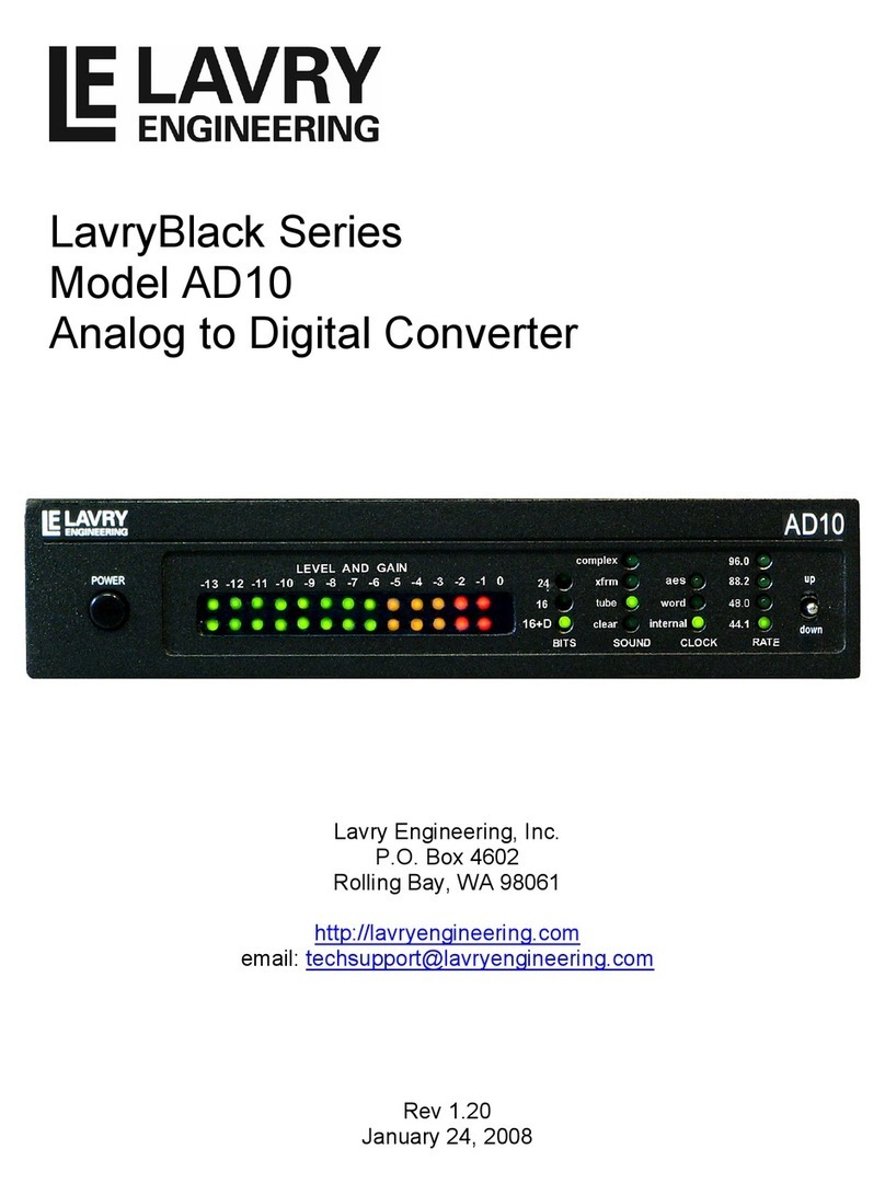
Lavry LavryBlack Series User manual

Lavry
Lavry AD11 User manual
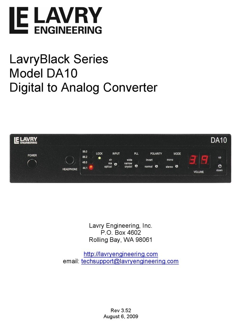
Lavry
Lavry DA10 User manual

Lavry
Lavry DA10 User manual
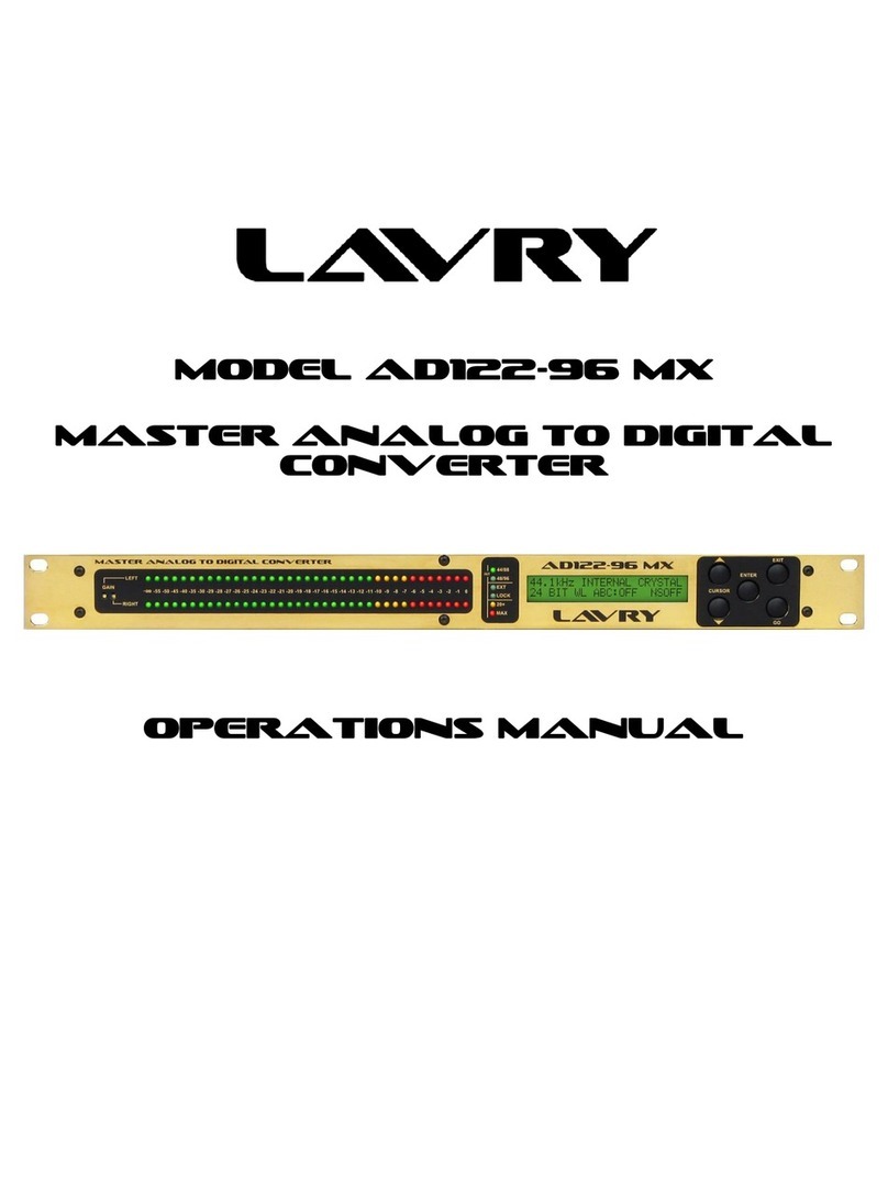
Lavry
Lavry AD122-96 MX User manual

Lavry
Lavry M AD-824 User manual
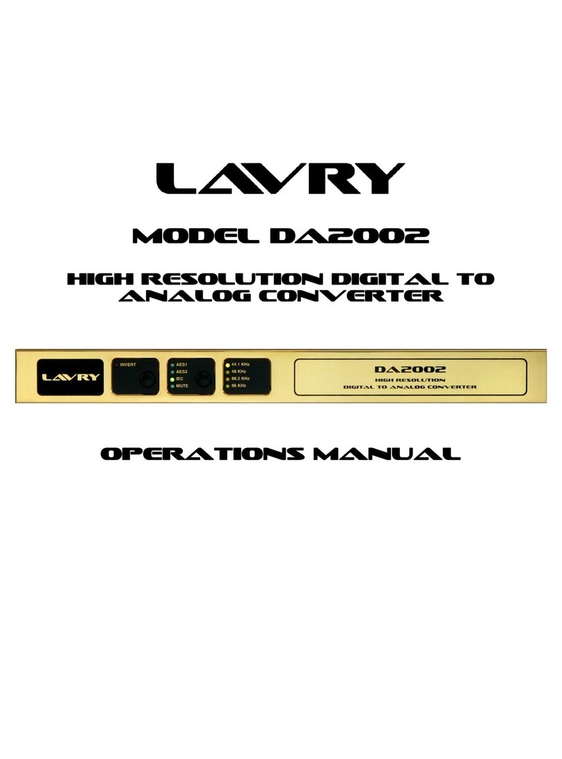
Lavry
Lavry DA2002 User manual

Lavry
Lavry DA924 User manual
Popular Media Converter manuals by other brands
PR electronics
PR electronics 4225 product manual
Antelope
Antelope AMARI user manual
Conrad
Conrad Grand Video Console Plus II operating instructions

Yamaha
Yamaha EZ-EG Short guide

Reliance
Reliance 13-030 installation instructions
Data Conversion Systems
Data Conversion Systems dCS Puccini U-Clock user manual
