LG KG110 User manual

launaMecivreS
:l
edoM KG110/KG115/MG110a/MG110b
Service Manual
KG110/KG115/
MG110a/MG110b
P/N : MMBD0061701 Date : Aug 2006 / Issue 1.0
KG110_Cover_Eng 2006.8.9 3:57 PM Page 1

1. INTRODUCTION......................................................................................................................3
1.1 Purpose ....................................................................................................................................3
1.2 Regulatory Information..............................................................................................................3
A. Security ..................................................................................................................................3
B. Changes in Service ................................................................................................................3
C. Maintenance Limitations ........................................................................................................3
D. Notice of Radiated Emissions ................................................................................................3
E. Interference and Attenuation ..................................................................................................4
F. Electrostatic Sensitive Devices................................................................................................4
2. SYSTEM SPECIFICATION......................................................................................................6
3. TECHNICAL BRIEF ................................................................................................................7
3.1 KG110 Block Diagram ..............................................................................................................7
3.2 RF Part Introduction..................................................................................................................8
3.2.1 Receiver Part......................................................................................................................8
A.Low Noise Amplifiers................................................................................................................9
B.Down-Converting Mixers..........................................................................................................9
C.Baseband Amplifiers / Low Pass Filters ................................................................................ 9
D.Baseband Output D.C. Offset Correction ..............................................................................10
E.Receiver Local Oscillator (LO) Generator..............................................................................10
3.2.2 Transmitter Part ..............................................................................................................10
A. Power Amplifier Module ........................................................................................................11
B.Quadrature Modulator............................................................................................................11
C.Phase Frequency Detector (PFD) ........................................................................................12
D.Loop filter ..............................................................................................................................12
E.TX VCO..................................................................................................................................12
F.Feedback Down-Converting Mixer ........................................................................................12
G.Transmit Frequency Plan ......................................................................................................12
H.Main Frequency Synthesizer ................................................................................................12
I.Fractional N Dividers ..............................................................................................................13
J.Phase Frequency Detector/Charge Pump..............................................................................13
K.Synthesizer Loop filter ..........................................................................................................13
L.Voltage Controlled Oscillator..................................................................................................13
3.2.3 The Crystal Reference System ........................................................................................13
3.2.4 Power Management ........................................................................................................14
A.LDO Usage............................................................................................................................14
3.3 Baseband Introduction ............................................................................................................15
3.3.1 Baseband Processor (AD6720 , U101)............................................................................15
3.3.2 Interconnection with external devices ..............................................................................15
A. RTC block interface ..............................................................................................................15
B. LCD module interface ..........................................................................................................16
C. RF interface..........................................................................................................................16
D. SIM interface ........................................................................................................................17
Table Of Contents
1

E. LDO Block ............................................................................................................................18
3.3.3 Battery Charging Block ....................................................................................................18
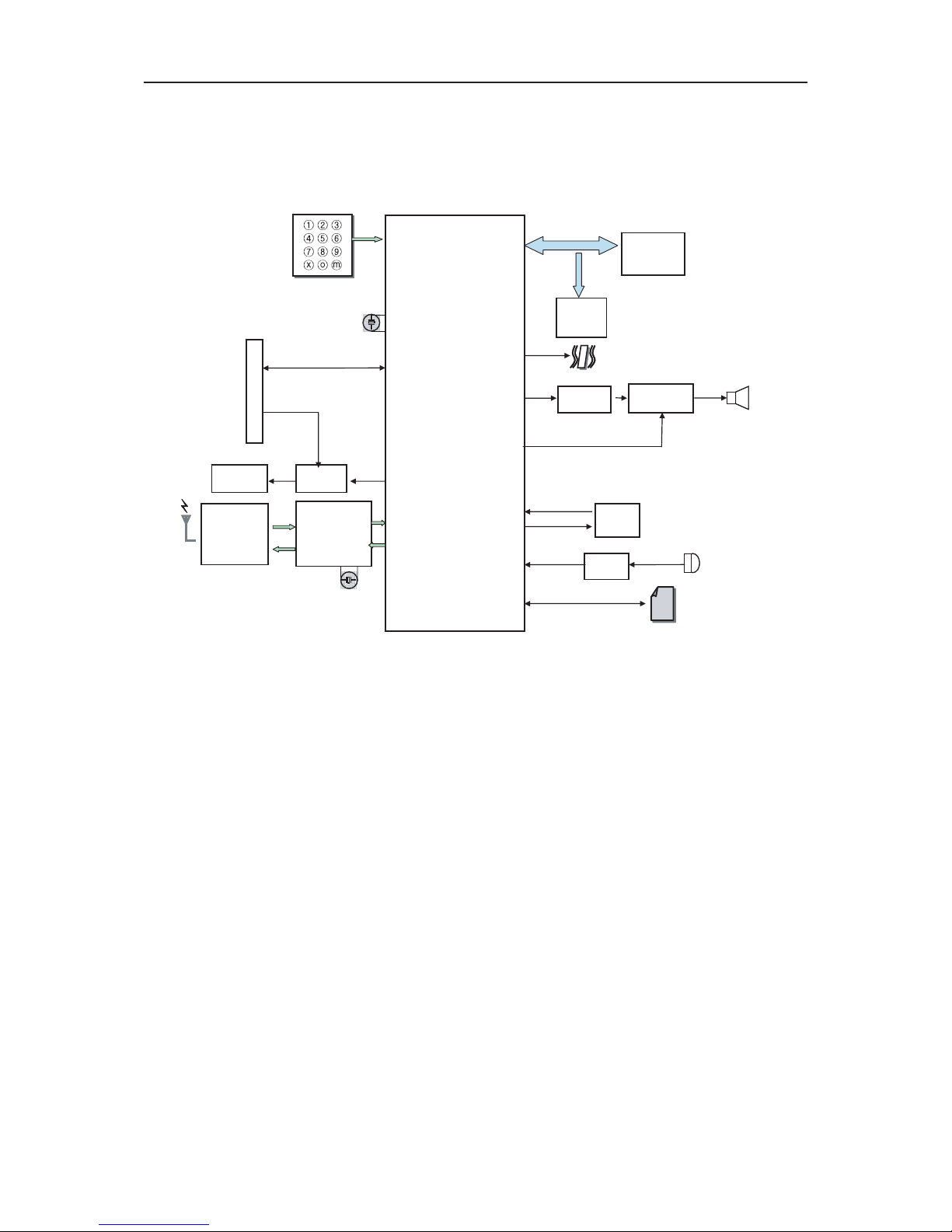
3.3.4 Display and Interface ......................................................................................................20
3.3.5 Keypad Switches and Scanning ......................................................................................21
3.3.6 Microphone...................................................................................................................... 22
3.3.7 Soft-midi and Main Speaker ............................................................................................23
3.3.8 Headset Interface ............................................................................................................24
3.3.9 Key Back-light Illumination ..............................................................................................25
3.3.10 LCD Back-light Illumination............................................................................................26
3.3.11 VIBRATOR......................................................................................................................26
4. Trouble shooting..................................................................................................................28
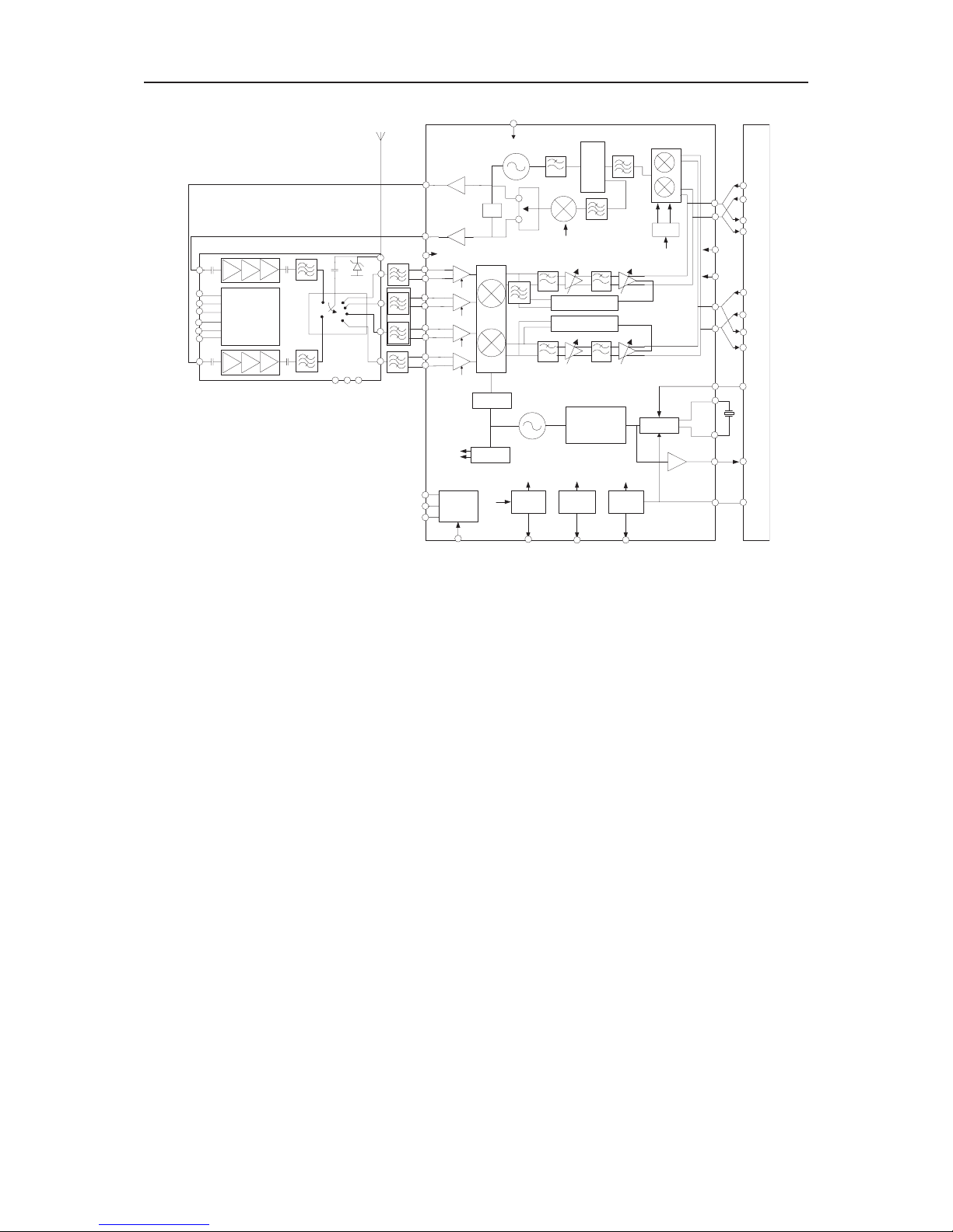
4.1 RF components ......................................................................................................................28
4.2 RX Trouble ..............................................................................................................................29
4.2.1 Check Crystal Circuit........................................................................................................30
4.2.2 Check Control Signal ......................................................................................................31
4.2.3 Check Mobile SW & ANT SW ..........................................................................................32
4.2.4 Check SAW filter..............................................................................................................34
4.2.5 Check I/Q signal ..............................................................................................................35
4.3 TX Trouble ..............................................................................................................................36
4.3.1 Check Crystal Circuit ......................................................................................................37
4.3.2 Check Control Signal ......................................................................................................38
4.3.3 Check TX I/Q signal ........................................................................................................39
4.3.4 Check PAM control signal ................................................................................................40
4.3.5 Check Mobile SW & ANT SW ..........................................................................................41
4.4 Power On Trouble ..................................................................................................................43
4.5 Charging Trouble ....................................................................................................................45
4.6 Download ..............................................................................................................................47
4.7 Calibration ..............................................................................................................................49
4.7.1 Equipment Setup..............................................................................................................49
4.7.2 Setup................................................................................................................................49
4.8 LCD Trouble............................................................................................................................56
4.8.1 LCD Blue Screen or abnormal display ............................................................................56
4.8.2 LCD Black Screen............................................................................................................57
4.9 Receiver Trouble ....................................................................................................................58
4.10 Speaker Trouble....................................................................................................................61
4.11 MIC Trouble ..........................................................................................................................63
4.12 Earphone Trouble..................................................................................................................65
4.13 KEYPAD Backlight LEDS Trouble ........................................................................................68
4.14 SIM Trouble ..........................................................................................................................69
5. Appendix ..............................................................................................................................71
1. BOM..........................................................................................................................................71
2. Exploded View ..........................................................................................................................80
3. Circuit diagram..........................................................................................................................82
4. Pcb layout..................................................................................................................................86
2

3
3
1. INTRODUCTION
1.1 Purpose
This manual provides the information necessary to repair, calibration, description and
download the features of KG110.
1.2 Regulatory Information
A. Security
Toll fraud, the unauthorized use of telecommunications system by an unauthorized part
(for example, persons other than your company’s employees, agents, subcontractors, or
person working on your company’s behalf) can result in substantial additional charges for
your telecommunications services. System users are responsible for the security of own
system.There may be risks of toll fraud associated with your telecommunications system.
System users are responsible for programming and configuring the equipment to prevent
unauthorized use. The manufacturer does not warrant that this product is immune from
the above case but will prevent unauthorized use of common – carrier telecommunication
service of facilities accessed through or connected to it. The manufacturer will not be
responsible for any charges that are resulted from such unauthorized use.
B. Changes in Service
A local telephone company may make changes in its communications facilities or
procedure. If these changes could reasonably be expected to affect the use of this phone
or compatibility with the network, the telephone company is required to give advanced
written notice to the user, allowing the user to take appropriate steps to maintain
telephone service.
C. Maintenance Limitations
Maintenance limitations on this model must be performed only by the manufacturer
or its authorized agent. Therefore, note that unauthorized alternations or repair may affect
the regulatory status of the system and may void any remaining warranty.
D. Notice of Radiated Emissions
This model complies with rules regarding radiation and radio frequency emission
as defined by local regulatory agencies. In accordance with these agencies,
you may be required to provide information such as the following to the end user.
1. INTRODUCTION

1. INTRODUCTION
4
E. Interference and Attenuation
Phone may interfere with sensitive laboratory equipment, medical equipment, etc.
Interference from unsuppressed engines or electric motors may cause problems.
F. Electrostatic Sensitive Devices

1. INTRODUCTION
ATTENTION
Boards, which contain Electrostatic Sensitive Device (ESD), are indicated by the
sign.
Following information is ESD handling :
• Service personnel should ground themselves by using a wrist strap when exchange
system boards.
• When repairs are made to a system board, they should spread the floor with anti-static
mat which is also grounded.
• Use a suitable, grounded soldering iron.
• Keep sensitive parts in these protective packages until these are used.
• When returning system boards or parts like EEPROM to the factory, use the protective
package as described.
5

2. SYSTEM SPECIFICATION
6
Item Target Specification
Form Factor Bar Type
Standard Battery (830mAh , Li-ion)
Size : 34(W) X 50(H) X 4.5(T) mm
Weight: 20g
Size 102.8 X 44 X 16.5mm
Weight 71 Gram(with standard battery)
Standby Current Below 3.0 mA under the least current consumption
(e.g. Paging Period = 9)
Talk Time Up to 3 hrs (GSM Tx Lev:5)
Standby Time Up to 200 hrs : Paging Period 9, RSSI 85dBm
Antenna Internal
LCD Main LCD: CSTN 128° X 128 Pixels 65K Color
Back Light Blue LED
PC Sync No
Indicator LED None
Vibrator Yes (Cylinder Type)
Buzzer Yes
C-MIC Yes
Receiver Yes
Earphone Jack Optional
SIM Socket Yes (SIM Block Type)
Volume Key No
Voice Key No
MP3/AAC No
MIDI 40 Poly Software MIDI
I/O Connector 24Pin
Basic Accessory Travel Adaptor

3. TECHNICAL BRIEF
3. TECHNICAL BRIEF
3.1 KG110 Block Diagram
Figure 3-1: KG110 Top Level Block Diagram
The Figure 3-1 shows the top level block diagram of KG110, it contains RF and BB part.
The following list is the detailed:
1. AD6720 : ADI baseband chipset,
including Digital Base Band (DBB) and Analog Base Band ABB
2.TQM6M4003 : Triquint PAM and Ant Switch
3. Transceiver : ADI Othello G AD6548
4. Flash: Spansion 128Mbit : 32Mbit
5. Others:
A. 22 keys
B. 128 x 128 65K CSTN –LCD module
C. Vibrator
D. Mic
E. Speaker and receiver
F. Ear-jack
G. Sim socket
H. Battery connector
7
BB Chip
AD6720
(Including
DBB and ABB)
LCD(65K)
Main 1.5”
TRANSCEIVER
Othello G
PAM + FEM
(TQM6M4003)
MIC
Circuit
Analog
Switch
830mAh
Li-Ion
Ear Mic
Charging
Circuit
SIM
SIM
Vibrator
24 Pin I/O Connector
Power
Serial Port
MIC
Key Pad
Speaker/RCV
Spansion
128Mbit Nor
+ 32M SRAM
Audio AMP
MAX9718
Memory Parallel
Interface
32.768k XTAL

3. TECHNICAL BRIEF
3.2 RF Part Introduction
The RF parts consists of a transmitter part, a receiver part, a voltage supply part,
the crystal reference system. And the main RF Chipset AD6548 is a highly integrated
direct conversion radio solution that combines, on a single chip, Quad Band Radio
(GSM850,E-GSM,DCS1800 and PCS1900 and power management functions necessary
to build the most compact GSM radio solution possible. This quad-band GSM transmit module
integrates a PA, a low-pass filter, a linear Tx / Rx switch along with PA and switch control
combined with ESD protection circuitry in one module,.
3.2.1 Receiver Part
The Receiver part in AD6548 contains all active circuits completely, full receiver chain
with the exception of discrete front-end RF SAW filters. The AD6548 uses direct
conversion receiver architecture of the OthelloTM family. For Quad band applicationsthe front
end features four fully integrated programmable gain differential LNAs. The RF is then
downconverted by quadrature mixers and then fed to the baseband programmable-gain
amplifiers and active filters for channel selection. The Receiver output pins can be directly
connected to the baseband analog processor. The Receive path features automatic calibration
and tracking to remove DC offsets. The RF Receiver block is shown as below.
8

3. TECHNICAL BRIEF
Figure 3-2: The RF Receiver Block
9
A. Low Noise Amplifiers
The AD6548 includes four fully integrated Low Noise Amplifiers (LNAs), to support quad band
applications without further external active components. The LNAs have differential inputs
which minimize the effect of unwanted interferers. The inputs are easily matched to industry
standard FEMs or discrete Rx SAW filters. The outputs of the LNAs are directly coupled to the
down-converting mixers. The voltage gain of the LNAs are typically 24 dB. Each LNA can be
switch to a low gain mode when receiving large input signals as part of the AGC system.
B. Down-Converting Mixers
Two quadrature mixers are used to mix down the signals from the LNAs, one for the
high bands (1800 and 1900 MHz) and one for the low bands (850 and 900 MHz).
The outputs of the mixers are connected to the baseband section through an integrated
single pole filter with nominal cut-off frequency of 800kHz. This acts as a “roofing filter”
for the largest blocking signals (i.e. those 3MHz) and prevents the baseband amplifiers
from being overloaded.
C. Baseband Amplifiers / Low Pass Filters
The baseband amplifiers provide the majority of the analog receiver gain.
The filtering is provided by an integrated 5th order Chebyshev filter giving the necessary adja-
cent channel and blocking filtering, it is also acting as an anti-alias filtering for Baseband IC’s
converters. A final low pass pole is possible at each of the baseband outputs via internal series
resistor along with an external shunt capacitor.
/2
PHD
/4
DC Offset
Correction
DC Offset
Correction
RX LO
Generator
Frac-N Synth VCTCXO
Serial
Interface
LDO
Reg 3
LDO
Reg 2
LDO
Reg 1
TX LO
Generator
Band
Control Tx_LO1
Tx_LO2
TX Loop filter
LNA Gain Reduction
TX_LO
2
TX_LO1
Supply
TX circuits
Supply
LO VCO
Supply
General
Supply
Ref
I
IB
VCC_BBI
VCC_BBQ
QB
Q
VAFC
REFINB
REFIN
REF_OP
VCC_REF
VDD
SEN
SCLK
SDATA
RX1900B
RX1900
RX1800B
RX1800
RX900B
RX900
RX850B
RX850
VCC_FE
TXOP_LO
TXOP_HI
VCC_TXVC
O
B
A
S
E
B
A
N
D
TXIB
TXI
RX
I
RXIB
TXQ
B
TX
Q
RX
Q
RXQB
AFC
REF_OP
CLK
Logic
&
Power
Control
ESD-
Diode
ANT
TX RF Output
RX RF Input
V1 Vcc1 Vcc2
(Internal Voltage)
DCS/PCS In
TX RF Input
Vbs1
Vbs2
Vtx
Vbatt
Vramp
Vmod_en
EGSM/GSM850 In
TX RF Input
ANT

3. TECHNICAL BRIEF
The external capacitor is not required with ADI baseband ICs. The on chip filter has an auto
calibration feature ensuring that the filters are tuned for optimum performance. The baseband
amplifiers have programmable gain for system AGC.
A total of 57 dB of gain control is provided in 3dB steps programmable over the serial
interface. This together with the LNA gain control gives a total of 77dB of gain control range.
The receive baseband outputs are routed to the common Rx/Tx I/Q ports for connection with
the baseband converters.
D. Baseband Output D.C. Offset Correction
In order to minimize D.C. offsets inherent in the receiver and maximize dynamic range
a D.C offset correction circuit is integrated. This correction is triggered over the serial bus
and then an offset tracking loop is enabled to minimize residual offsets under all conditions.
The tracking loop is fully hardware integrated, requiring no software intervention.
E. Receiver Local Oscillator (LO) Generator
The Rx LO generator is used to avoid DC offset problems associated with LO leakage
into the receiver RF path. By operating the VCO at a frequency other than the desired
receive frequencies,any leakage of the VCO (e.g. via package) will fall out of band.
The LO generator is used to convert the offset synthesized VCO output to the
on-frequency quadrature LO required by the chipset.
The LO generator is implemented as a regenerative frequency divider, performing a 2/3
multiplication of the VCO output for the high band (DCS1800/PCS1900) and a 1/3
multiplication for low band (E-GSM/GSM850).
3.2.2 Transmitter Part
The Transmitter part contains AD6548 active parts and PAM .
The transmit section of the AD6548 radio implements a translation loop modulator.
This consists of a quadrature modulator, high speed phase-frequency detector (PFD) with
charge pump output, loop filter, TX VCO and a feedback down converting mixer.
The VCO output (divided by 2 for low band) is fed to the power amplifier with a portion
internally fed back into the down-converting feedback mixer to close the feedback loop.
10

3. TECHNICAL BRIEF
A. Power Amplifier Module
11
Figure 3-3: Power Amplifier Module
Table 3-1: PAM Truth Table
The advanced quad-band Transmit Module designed for mobile handset applications
provides full RF transmit functionality.The GSM850/900 and DCS/PCS power amplifier
blocks including power control are combined with the low insertion loss quad-band
pHEMT switch, Tx harmonics filtering, integrated switch decoder, four receive ports,
and full ESD protection. This architecture eliminates the need for any PA-to-switch design
effort for phone designers. All four Rx ports are frequency independent and allow flexible
routing to the transceiver. Fabricated in high-reliability InGaP HBT / pHEMT technology, the
module supports GPRS class 12 operation and provides 50 Ohms input and output
impedances at all RF input and output ports. The module control inputs are CMOS
compatible and has no need for an external reference voltage. With its excellent efficiency
performance in all 4 bands, the power amplifier and switch module contributes to the overall
talktime targets of next generation mobile handset designs.
B. Quadrature Modulator
The Quadrature modulator takes the baseband I & Q signals and translates these into a GMSK
signal at the Transmit Intermediate Frequency (TX IF). After bandpass filtering and limiting the
TX IF signal is used as the reference input to the Phase Frequency Detector (PFD) of the
transmit PLL.
Control Voltage
Operating
Mode Vmod_en Vtx Vbs1 Vbs2
TX GSM 850/900 H H L L
TX DCS/PCS H H H L
RX1 H L L L
RX2 H L L H
RX3 H L H L
RX4 H L H H
Sleep Mode L L L L

3. TECHNICAL BRIEF
C. Phase Frequency Detector (PFD)
The PFD ensures that the transmitted signal contains the required modulation and is
accurately locked to the desired GSM channel. The downconverted feedback signal from
the TXVCO and the Quadrature Modulator output are phase compared by the PFD.
The PFD charge pump generates a current pulse proportional to the difference in phase
which is applied to the loop filter.
D. Loop filter
To minimize complexity of the external PCB layout the TX loop filter is fully integrated into
the IC. At power up the filter is automatically calibrated as part of the baseband filter cal,
eliminating process tolerances. The calibration is fully integrated and requires no
extra programming.
E.TX VCO
The Transmit Voltage Controlled Oscillator (TX VCO) and tank components are a fully
integrated subsystem. The subsystem includes PA drivers so the outputs are used to directly
drive the external PAs. The low noise oscillator design and internal filtering mean that external
TX SAW filters are not required. In Low band operation the TX VCO output is divided by two
and filtered. The TX VCO is automatically calibrated to ensure optimum performance over its
operating frequency of 1648 to 1910 MHz.
F. Feedback Down-Converting Mixer
The feedback down converting mixer is used to translate the TX VCO output frequency to
the TX IF. An integrated band pass filter exists between the mixer and the PFD to filter the
mixers unwanted side band and higher order mixing products.
G.Transmit Frequency Plan
Unlike many other translation loop modulators the AD6548 uses only a single VCO source to
derive the local oscillator signal for both the Feedback Down-Converting Mixer and the
Quadrature modulator. Therefore there is a fixed relationship between the Tx IF frequency and
the LO VCO frequency .This ratio was chosen to minimize VCO tuning range, TX IF frequency
variation and ensure excellent transmit spectral mask performance. The Feedback-Down
Converting Mixer operates low side injection for the high bands and high side injection for the
low bands. The final relationship between the transmitted TX frequency frequency and the LO
VCO frequency is different between the two bands. These relationships are taken account of in
the synthesizer architecture and programming.
H. Main Frequency Synthesizer
The AD6548/9 has a single fast-locking fractional synthesizer used for VCO control in both
receive and transmit mode. The entire system including VCO, tank, fractional N dividers,
sigma delta compensation, charge pump and loop filters are fully integrated.
The only external component is a low cost crystal for the reference.
The synthesizer is controlled via the serial interface. The VCO is fed into the respective
dividers to generate the appropriate LO frequencies for the RX and TX bands.
I. Fractional N Dividers
The fractional N divider allows the PLL system to have a smaller step size than the
comparison frequency which is set by the external reference to 26 MHz.
This feature allows all the GSM frequency band rasters to be achieved, with fast lock times
and good phase noise characteristics. The divider section consists of a dual modulus 8/9
12

3. TECHNICAL BRIEF
prescaler, integer M & A dividers, and fractional N system based on sigma-delta modulation
to generate the required fractional divide ratio. The Denominator of the fractional divider can
be set to 3 different values, (1040, 1170, 1235), depending on the mode of operation.
For example a denominator of 1040 with an input fraction F maintains an average value of
F/1040 allowing 25 kHz steps when operated at a reference of 26 MHz.
J. Phase Frequency Detector/Charge Pump
A Phase Frequency Detector (PFD) is used for the PLL phase detector.
The charge pump is designed such that good matching of up and down currents is
achieved over a wide output operating range. The charge pump output is internally routed to
the integrated synthesizer loop filter.
K. Synthesizer Loop filter
To minimize complexity of the external PCB layout the Main Synthesizer loop filter
is also fully integrated into the IC. No external components or adjustments are required .
L.Voltage Controlled Oscillator
The integrated voltage controlled oscillator (VCO) is a complete self-calibrating
subsystem. This employs a fully automated digital self-calibration function to
ensure optimum phase noise performance over the entire frequency range.
The VCO generates frequencies between 2520MHz and 2985MHz as required to operate in
the four bands for RX and TX.
3.2.3 The Crystal Reference System
The AD6548 requires only an external low cost crystal as the frequency reference.
The circuitry to oscillate the crystal and tune its frequency is fully integrated.
The Oscillator is a balanced implementation requiring the crystal to be connected
across 2 pins. There is a programmable capacitor array included for coarse tuning
of fixed offsets (e.g. crystal manufacturing tolerance), and an integrated varactor for
dynamic control. The oscillator is designed for use with a 26MHz crystal.
The crystal is connected as shown in figure.
13
Figure 3-4: The Crystal Reference System
Dedicated control software ensures excellent frequency stability under all
circumstances.
VCTCXO
Supply
Ref
VAFC
REFINB
REFIN
REF_OP
VCC_REF
AFC
REF_OP
CLK

3. TECHNICAL BRIEF
3.2.4 Power Management
For direct battery supply connect, and to reduce external circuitry complexity the AD6548/9
features three Low Drop Out Regulators (LDOs). The three LDOs provide isolation of the
oscillators and sensitive circuits from unwanted power supply and cross coupled noise.
They also ensure the IC operation is robust over a wide range of power supply voltages.
For power management the LDOs are independently controlled via the 3 wire serial bus.
A.LDO Usage
The following table describes the LDO usage:
14
LDO1 LDO2 LDO3
Rx and Tx baseband Main VCO TX VCO
sections
LDO OP External Connection
VLDO1 VCC_FE, VCC_BBI, VCC_BBQ
VLDO2 No external Connections, except for decoupling
VLDO3 No external Connections, except for decoupling
Table 3-2: Intended LDO Use
Table 3-3: LDO Connections
The LDO outputs require external connection to the respective pins described in table 3, and
each requires decoupling capacitors.The LDOs are designed to be unconditionally stable
regardless of the capacitor's ESR.
LDO1 derives its input references from the crystal supply voltage (VCC_REF).
It is therefore expected that VCC_REF be supplied from a external LDO of nominal supply
voltage 2.75V
(e.g. ADP3330 or Analog Baseband IC: Vout=2.75V 1.4%)

3. TECHNICAL BRIEF
3.3 Baseband Introduction
3.3.1 Baseband Processor (AD6720 , U101)
• AD6720 is an ADI designed processor
• AD6720 consists of
1. Control Processor Subsystem including:
• 32-bit MCU ARM7TDMI Control Processor
• 39 MHz operation at 1.8V
• 1Mb of on-chip System SRAM Memory
2. DSP Subsystem including:
• 16-bit Fixed Point DSP Processor
• 91 MIPS at 1.8V
• Data and Program SRAM
• Program Instruction Cache
• Full Rate, Enhanced Full Rate and Half Rate
• Speech Encoding/Decoding
• Capable of Supporting AMR & PDC Speech Algorithms
3. Peripheral Functions
• Parallel and Serial Display Interface
• Keypad Interface
• Flash Memory Interface
• Page-Mode Flash Support
• 1.8V and 3.0V, 64 kbps SIM Interface
• Universal System Connector Interface
• Data Services Interface
• Battery Interface (e.g. Dallas)
4. Other
• Supports 13 MHz and 26 MHz Input Clocks
• 1.8V Typical Core Operating Voltages
• 289-Ball Package (12x12mm) , 0.65mm Ball pitch
5. The AD6720 baseband transmit section supports the following
• mobile station GMSK modulation power classes:
• GSM 900/850 power classes 4 and 5,
• DCS 1800 power classes 1 and 2, and
• PCS 1900 power classes 1 and 2
15

3. TECHNICAL BRIEF
3.3.2 Interconnection with external devices
A. RTC block interface
Countered by external X-TAL
The X-TAL oscillates 32.768KHz
B. LCD module interface
16
Signals Description
L_MAIN_LCD_CS MAIN LCD driver chip enable.
LCD_RESET This pin resets LCD module.
LCD_WR Enable writing to LCD Driver.
LCD_RD Enable reading to LCD Driver.
LCD_RS This pin determines whether the data to LCD module
data or control data.
A1 Select 16bits interface mode for MAIN LCD.
Signals Description
LCD_LED_CTL Control LCD backlight level in 4 steps
DISP_LIGHT Current source for backlight LED
Signals Description
PA_BAND (GPO17) PAM Band Select
ANT_SW1 (GPO9)Antenna switch Band Select
ANT_SW2 (GPO11) Antenna switch Band Select
RF_PWR_DWN(GPO 4) Power down Input
CLKON RF LDO Enable/Disable
Table 3-4: LCD Pin Description
Table 3-5. Description Of LCD Backlight LED Control
The backlight of LCD module is controlled by AD6720 via AAT3110 , U300.
The control signals related to Backlight LED are given bellow.
C. RF interface
The AD6720 control RF parts through PA_BAND, ANT_SW1, ANT_SW2, ANT_SW3 ,
CLKON ,PA_EN, S_EN, S_DATA, S_CLK, RF_PWR_DWN.

3. TECHNICAL BRIEF
D. SIM interface
The AD6720 provides SIM Interface Module. The AD6720 checks status periodically
during established call mode whether SIM card is inserted or not, but it doesn't check
during deep Sleep mode. In order to communicate with SIM card, 3 signals SIM_DATA,
SIM_CLK, SIM_RST(GPIO_23) are required.
The descriptions about the signals are given by bellow Table 3-7 in detail.
17
Signals Description
PA_EN (GPO16) PAM Enable/Disable
S_EN (GPO19) PLL Enable/Disable
S_DATA (GPO20) Serial Data to PLL
S_CLK (GPO21) Clock to PLL
Signals Description
SIM_DATA This pin receives and sends data to SIM card.
This model can support only3.0 volt interface SIM card.
SIM_CLK Clock 3.25MHz frequency.
SIM_RST Reset SIM block(GPIO_23)
Table 3-6. RF Control Signals Description
Table 3-7: SIM Control Signals Description

3. TECHNICAL BRIEF
E. LDO Block
There are 8 LDOs in the AD6720.
- VCORE : supplies Digital base band Processor core and AD6720 digital core
- VMEM : supplies external memory and the interface to the external memory on the digital
base band processor (1,8V or 2.8V, 150mA)
- VEXT : supplies Radio digital interface and high voltage interface (2.8V, 170mA)
- VSIM : supplies the SIM interface circuitry on the digital processor and SIM card (2.85V,
20mA)
- VRTC : supplies the Real-Time Clock module (1.8 V, 20 mA)
- VABB : supplies the analog portions of the AD6720
- VMIC : supplies the microphone interface circuitry (2.5 V, 1 mA)
- VVCXO : supplies the voltage controlled crystal oscillator ( 2.75 V, 10 mA)
3.3.3 Battery Charging Block
1. It can be used to charge Lithium Ion batteries.
Charger initialization, trickle charging, and Li-Ion charging control are implemented
in hardware.
2. Charging Process
- Check charger is inserted or not
18
Figure 3-5: SIM Interface of AD6720
SIMCLK
SIMRESET
VSIM
R341
20K
C326 NA
VCC 1
RST 2
CLK 3
GND
5
VPP
6
IO
7
J300
SCK-6S-12PT-TF
SIMDATAOP
VSIM
C327 220n
R345 0
C329 1000p
C328 NA
C321
2.2u
(1608)

3. TECHNICAL BRIEF
- If AD6720 detects that Charger is inserted, the CC-CV charging starts.
- Exception : When battery voltage is lower than 3.2V, the precharge
(low current charge mode) starts firstly.
- And the battery voltage reach to 3.2V the CC-CV charging starts.
3. Pins used for charging
- VCHG : charger supply.
- GATEDRIVE : charge DAC output
- ISENSE : charge current sense input
- VBATSENSE : battery voltage sense input.
- BATTYPE : battery type identification input
- REFCHG : voltage reference output
4. TA (Travel Adaptor)
- Input voltage: AC 85V ~ 260V, 50~60Hz
- Output voltage: DC 5.2V ( 0.2 V )
- Output current: Max 800mA ( 50mA )
5. Battery
- Li-ion battery (Max 4.2V, Nom 3.7V)
- Standard battery: Capacity - 830mAh
19
VCHARGE VBAT
PRE_CHARGE
R344
1K
C322
1U
R349
100K
R348
20K 1 6
3
2 5
4
Q300
UMX1NTN
R266
NA
R342
33
PRECHARGE
Other manuals for KG110
4
This manual suits for next models
3
Table of contents
Other LG Cell Phone manuals