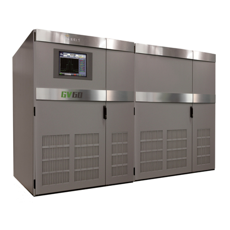
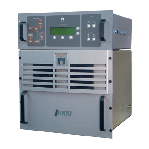
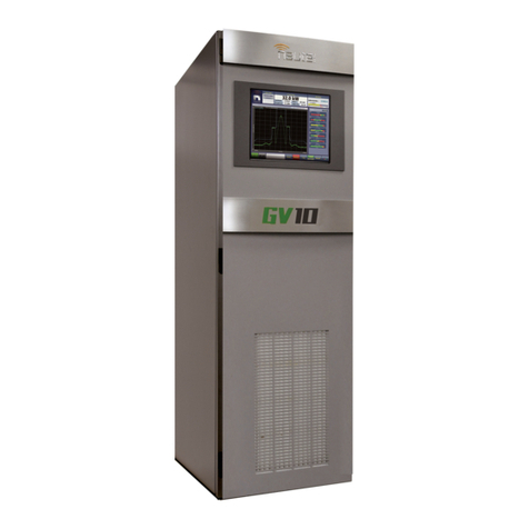
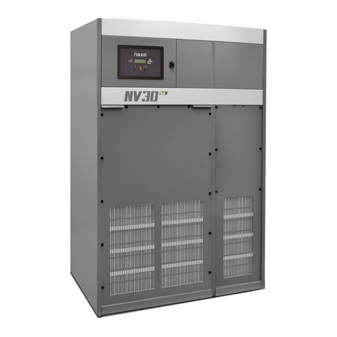
Nautel GV5 Manual

3: OPERATIONS & MAINTENANCE
MANUAL
GV5/GV3.5
TRANSMITTER
Document ID: NHB-GV3.5-GV5-OPS
Version: 0.2
Issue Date: 2014-07-23
Status: Preliminary
Making Digital Radio Work


VERSION 0.2 2014-07-23 PAGE III
GV5/GV3.5 OPERATIONS & MAINTENANCE MANUAL
Contact Information
Nautel Limited
10089 Peggy’s Cove Road
Hackett’s Cove, NS Canada B3Z 3J4
Toll Free: +1.877.6NAUTEL (662.8835)
(Canada & USA only) or
Phone: +1.902.823.3900 or
Fax: +1.902.823.3183
Nautel Inc.
201 Target Industrial Circle
Bangor, Maine USA 04401
Phone: +1.207.947.8200
Fax: +1.207.947.3693
Customer Service (24-hour support)
+1.877.628.8353 (Canada & USA only)
+1.902.823.5100 (International)
Email: [email protected]
Web: www.nautel.com
The comparisons and other information provided in this document have
been prepared in good faith based on publicly available information.
For verification of materials, the reader is encouraged to consult the
respective manufacturer's most recent publication on the official
website or through contact with Customer Service.
© Copyright 2013 NAUTEL. All rights reserved.


GV5/GV3.5 OPERATIONS & MAINTENANCE MANUAL TABLE OF CONTENTS
VERSION 0.2 2014-07-23 PAGE 3.V
CONTENTS
Contact Information 3.iii
RELEASE CONTROL RECORD 3.vii
Description 3.1.1
Ac-Dc Power Stage 3.1.1
Control/Monitor Stage 3.1.3
RF Drive Stage 3.1.4
RF Power Stage 3.1.5
Operating the Transmitter 3.2.1
User Interface Options 3.2.4
Advanced User Interface (AUI) 3.2.9
Controller Front Panel 3.2.17
Home Page 3.2.24
Viewing Transmitter Log 3.2.27
Viewing Tool Menu Panels 3.2.37
Viewing Real-Time Meters 3.2.53
Presets - Editing Operational Settings 3.2.60
Resetting Alarms 3.2.98
Viewing Transmitter Status - using the AUI 3.2.99
System Settings 3.2.101
User Accounts 3.2.130
Changing Exciter Transfer Settings 3.2.134
User Settings - AUI 3.2.137
User Settings - Controller UI 3.2.166
Configuring Remote Inputs and Outputs 3.2.173
Preset Scheduler 3.2.187
Audio Player 3.2.190

GV5/GV3.5 OPERATIONS & MAINTENANCE MANUAL TABLE OF CONTENTS
PAGE 3.VI VERSION 0.2 2014-07-23
Enabling and Operating the Orban Audio Processor 3.2.196
Routine Maintenance 3.3.1
Scheduled Maintenance 3.3.1
Replacing an Air Filter 3.3.3
Performing On-Air Checks 3.3.6
Replacing the Controller Module’s Battery 3.3.7
Inspecting Lightning Protection Systems 3.3.9
Non-standard maintenance 3.4.1
Upgrading Software 3.4.1
Configuring a Mod Loss Backup Preset 3.4.4
List of terms 3.5.1

GV5/GV3.5 OPERATIONS & MAINTENANCE MANUAL
VERSION 0.2 2014-07-23 PAGE 3.VII
RELEASE CONTROL RECORD
ISSUE DATE REASON
0.1 2013-04-04 Preliminary Release of GV5/GV3.5 (NARF71A/02)
0.2 2014-07-23 Updated Section 2: Operating the Transmitter for software
version 4.1; added information for Xmtr PA Bias routine

GV5/GV3.5 OPERATIONS & MAINTENANCE MANUAL
PAGE 3.VIII VERSION 0.2 2014-07-23

GV5/GV3.5 OPERATIONS & MAINTENANCE MANUAL DESCRIPTION
VERSION 0.2 2014-07-23 PAGE 3.1.1
SECTION 3.1: DESCRIPTION
This section provides a high-level description of the transmitter’s key sections. The transmitter circuitry
is subdivided into four basic stages:
Ac-Dc Power Stage
Control/Monitor Stage - see page 3.1.3
RF Drive Stage - see page 3.1.4
RF Power Stage - see page 3.1.5
Refer to the functional block diagrams: Figure 3.1.1 on page 3.1.9 (GV5/GV3.5 transmitter) and Figure
3.1.2 on page 3.1.10 (audio path).
GV5/GV3.5 Electrical Schematics
Some descriptions in this section refer to electrical schematics (SD-#s) . These are located in Section 4 of
the GV5/GV3.5 Troubleshooting Manual.
Ac-Dc Power Stage
See electrical schematic Figure SD-1. The ac-dc power stage provides power to operate the low voltage
power supplies, which generate the 40 to 48 V dc voltage that is converted to the low level dc voltages
(±15 V and +5 V) used throughout the transmitter. This voltage is also conditioned to operate cooling
fans in the RF power module and reject load assemblies. The ac-dc power stage also converts the ac
power source to a positive dc voltage (PA volts) for the transmitter's RF power amplifiers and exciter(s).
The transmitter accepts a wide range of ac input voltage options:
3-phase, 180 - 264 V ac (208 V ac nominal)
3-phase, 312 - 457 V ac (380 V ac nominal)
1-phase, 180 - 264 V ac (240 V ac nominal)
The ac-dc power stage comprises ac input terminal block TB1, power supply interface PWB (A1), low
voltage power supply (LVPS) modules A (U2), B (U3), and power supply modules (U4 through U7), two
for each of the two RF power modules. There are three amber LED pilot lamps (DS1 through DS3),
located in the bottom, rear of the cabinet, that indicate the presence of each ac phase.

GV5/GV3.5 OPERATIONS & MAINTENANCE MANUAL DESCRIPTION
PAGE 3.1.2 VERSION 0.2 2014-07-23
Power Supply Interface PWB
See electrical schematic Figure SD-1. The power supply (PS) interface PWB (A1):
interfaces between the ac input on terminal block TB1 and the LVPS and power supply
modules.
distributes LVPS voltage to the RF drive (exciter) stage and the control/monitor stage.
distributes PA voltage to the RF power stage and the control/monitor stage.
controls, with the controller module, the LVPS output voltage.
provides RS485 serial communication between the module control/interface PWB and the RF
power module power supplies.
allows configuration of the LVPS modules if the UPS option is installed.
provides status and alarm outputs from the LVPS and power supply modules, consisting of
Module Present, Power Fail Warning, Rectifier Fault and Overtemp Warning (provided to the
module control/interface PWB over a serial bus).
LVPS Modules
See electrical schematic Figure SD-1. LVPS modules A (U2) and B (U3) convert the ac input voltage to
the regulated output (40 - 48 V dc, nominally 40 V) that is applied to, and controlled by, the controller
module via the module control/interface PWB. +5 V, +15 V and -15 V regulated outputs are developed
from the LVPS output voltage (40 - 48 V dc) on the module control/interface PWB.
Power Supply Modules
See electrical schematic Figure SD-1. Power supply modules U4 through U7 convert the ac input voltage
to a regulated dc supply (PA volts) for both RF power modules. Each switching power supply module is
rated for a nominal 2725 W and provides an output voltage between 18 V and 53 V (typically 40 V). The
modules regulate the output voltage based on a serial control input from the controller module (A4),
applied via the module control/interface PWB. Each module has a built-in cooling fan, senses excessive
temperature conditions and applies an Overtemp Warning signal (for indication purposes only) to the
module control/interface PWB. The module also senses out-of-regulation on the ac input and dc output,
and applies a Power Fail Warning signal to the module control/interface PWB. Both conditions cause the
power supply to shut itself down, thus reducing the transmitter's RF output. All power supply module
signals are applied to the controller for system level monitoring.
GV5/GV3.5 OPERATIONS & MAINTENANCE MANUAL DESCRIPTION
VERSION 0.2 2014-07-23 PAGE 3.1.3
Control/Monitor Stage
See electrical schematic Figure SD-2. The control/monitor stage performs many critical functions for the
transmitter. It:
contains monitoring and protection circuits to prevent transmitter damage under adverse or
fault conditions, including high speed SWR protection and interlock/muting.
monitors the current value of various parameters including cooling fan tachometer outputs,
transmitter output forward and reflected power, module temperature, PA current levels, and
PA power supply status signals.
measures and monitors the output voltage from the power supply modules as well as the low
voltage power supplies.
generates the signals that enable the power supply modules and control their output voltage.
provides the status of any controller fault conditions.
contains an integral DSP that performs all audio processing including filtering and FM
baseband modulation.
interfaces with the RF and power supply sections of the transmitter to perform control and
monitoring functions.
provides local and remote interfacing for the transmitter. Local interfacing is performed via
the local AUI touch screen on the front door of the transmitter and the controller module’s
front panel UI - a 4 x 20 graphic LCD display - and its adjacent keypad. The AUI and controller
UI each contain a menu-based series of pages that serve specific functions. The AUI is also
available via remote access. The AUI is a flash graphic that can be used on any web-based PC
or handheld device. The remote interface PWB (A16) allows the user a more convenient
method to interface with the transmitter from a remote location using discrete wiring.
The primary components of the control/monitor stage are the single-board computer (A4A1) and
controller PWB (A4A1), which are part of the controller module (A4) and the module control/interface
PWB (A3).
The UI interface PWB (A4A2), also part of the controller module, provides an interface between the
controller UI and the module control/interface PWB (A3). It also contains the pushbutton switches (RF
ON, RF OFF and LOCAL/REMOTE) and associated status LEDs that protrude through the front panel,
adjacent to the UI.
The remote interface PWB (A16) provides a convenient method to remotely control and monitor of the
transmitter. It contains push-button switches that provide backup control for the RF on/off, local/
remote, power increase/decrease and reset functions. It also contains LEDs that serve as an alternate
means to monitor status (local/remote and RF on/off) and various status and alarm parameters.

GV5/GV3.5 OPERATIONS & MAINTENANCE MANUAL DESCRIPTION
PAGE 3.1.4 VERSION 0.2 2014-07-23
RF Drive Stage
See electrical schematic Figure SD-3. The RF drive stage converts the exciter's RF output to the
intermediate RF level needed to drive the RF power modules. It consists of exciter A (A5), optional
exciter B (A6) and RF drive splitter/changeover assembly (A7).
Exciter(s)
Exciter A (A5) and B (A6, optional) are the RF drive sources for the transmitter. They accept the external
audio program information (see the GV5/GV3.5 Pre-installation Manual for details on various program
input types). For dual exciter applications, the exciters’ main/standby operation is controlled using the
local (or remote) AUI or the controller UI. The exciter outputs are applied to the RF drive splitter/
changeover assembly (A7). The exciter provides a nominal RF drive signal of 11 W (in analog mode).
RF Drive Splitter/Changeover Assembly
See also electrical schematic Figure SD-33. The RF drive splitter/changeover assembly (A7) controls the
routing of the main exciter and, if applicable, the standby exciter and provides the RF drive signals for
the two RF power modules. The assembly is comprised of the splitter/changeover PWB (A7A1) and the
2-way RF drive splitter/attenuator PWB (A7A2).
Exciter Relay Control - Dual Exciters Only
The RF drive outputs from exciters A and B are applied to the RF drive splitter/changeover assembly at
A7A1J1 and A7A1J2 respectively. The Exciter Relay Control input (A7A1J3-4) is a signal applied from
the control/monitor stage that controls relay A7A1K1.
When exciter A is selected as the main RF drive source, the Exciter Relay Control input is open
circuit and relay A7A1K1 will be de-energized. Exciter A's output will be applied to 3 dB
hybrid coupler A7A1U1.
When exciter B is selected as the main RF drive source, the Exciter Relay Control input is near
ground potential (0 V) and relay A7A1K1 will be energized. Exciter B's output will be applied
to 3 dB hybrid coupler A7A1U1.
Exciter Drive Splitter
The splitter/changeover PWB’s 3 dB hybrid coupler (A7A1U1) is connected as a splitter. The RF drive
source (A or B) selected by relay A7A1K1 is applied to A7A1U1’s input. The signal is split into two equal
amplitude signals that are 90° out-of-phase. These split signals are applied to 2-way RF drive splitter/
attenuator PWB A7A2.

GV5/GV3.5 OPERATIONS & MAINTENANCE MANUAL DESCRIPTION
VERSION 0.2 2014-07-23 PAGE 3.1.5
2-Way RF Drive Splitter/Attenuator
The 2-way RF drive splitter/attenuator PWB (A7A2) accepts the outputs from the splitter/changeover
PWB’s 3 dB hybrid coupler and splits it into two equal amplitude signals, using two 3 dB couplers
identical to A7A1U1. The outputs of the 3 dB couplers are applied to attenuators, as required, for
application to the two RF power modules. Attenuation values are set in order to balance the RF drive
output levels.
RF Power Stage
See electrical schematic Figure SD-4. The RF power stage accepts the intermediate RF drive inputs from
the RF drive stage and generates the final RF output. It consists of two RF power modules, the module
control/interface PWB (A3), a 10 kW combiner/filter (A12), an output power probe (A15), a 2-input
reject load assembly (A13) and a 2-way fan tray assembly (A14).
RF Power Module
See electrical schematic Figure SD-34. Each of the two RF power modules provides up to 3000 W (for
GV5) or 2250 W (for GV3.5) of RF output power. Each module contains four power amplifier (PA) PWBs
(A1 through A4), a splitter/interface PWB (A5), combiner PWBs (A6 and A7), and six cooling fans. The
intermediate RF drive outputs from the RF drive stage are applied to the RF power modules via the
module control/interface PWB (A3). Within each RF power module, the RF drive signal is sampled and
then split to drive the module's four PAs. The PA Volts inputs from the associated power supply modules
control the RF output of the four PAs.

GV5/GV3.5 OPERATIONS & MAINTENANCE MANUAL DESCRIPTION
PAGE 3.1.6 VERSION 0.2 2014-07-23
Module Control/Interface PWB
See also electrical schematics Figures SD-9 through SD-16. The module control/interface PWB:
interfaces with all RF power module inputs and outputs, except for the RF output.
interfaces between the controller module (A4) and the rest of the transmitter, distributing
forward and reflected power samples, exciter control signals, and metering for reject load
assemblies and the RF drive splitter/changeover assembly.
distributes RF drive power, PA voltage and PA bias voltage to the RF power modules.
monitors critical parameters of the RF power modules, such as RF drive sample, reject power
sample, heatsink temperature and cooling fan speed. Monitoring circuits determine if a
parameter is out of tolerance and generate the necessary control signal to compensate for the
out of tolerance condition or to inhibit the RF power module’s associated power supplies.
applies control signals to the power supply modules fromthe controller and also monitors
status signals and critical meters from the power supply modules and applies them to the
controller. The controller can inhibit the power supply modules, as necessary (RF off, PS Temp
alarm), or enable the power supply modules (RF on).
generates a sample of the PA voltage applied to each RF power module and applies it to the
control/monitor stage.
samples the RF power module meters and generates the necessary PA bias voltages for each
RF power module’s PAs.
Combiner/Filter
The 5 kW combiner/filter (A12) accepts the RF outputs from two RF power modules and uses a 3 dB
hybrid coupler to provide a single RF output. The 3 dB hybrid coupler accepts the outputs of two RF
power modules. The equal amplitude, 90° out-of-phase (quadrature) RF signals are combined at the 3
dB hybrid coupler output and applied to a 5 kW low pass filter before being applied to the output
power probe (A15).
Any amplitude or phase imbalance betweenthe 3 dB hybrid coupler inputs causes a proportional signal
to be applied to the reject load assembly’s 5kW Rej Ld Pwr (1/2) via J5.

GV5/GV3.5 OPERATIONS & MAINTENANCE MANUAL DESCRIPTION
VERSION 0.2 2014-07-23 PAGE 3.1.7
Reject Load Assembly
The reject load assemby (A13) provides a means to dissipate reject power from the outputs of the
combiner/filter's 3 dB hybrid couplers. The reject load assembly contains power resistors to dissipate
reject power. Cooling air for the reject load assembly is provided by fans in the fan tray assembly (A14).
The module control/interface PWB (A3) monitors the speed of the cooling fans and regulates the
voltage being applied to them accordingly.
Reject power generated by the combining stage of the combiner/filter is dissipated by resistors in the
1-input reject load assembly. Micro-strip transmission lines (on 2-input reject load PWB A13A1) in close
proximity to the reject load signals induce one true RF sample voltage of the associated reject power.
This sample is peak detected and applied to the control/monitor stage via the module control/interface
PWB (A3). The module control/interface PWB provides an interface between the ac-dc power stage’s
Rej Fan Volts supply and the fan tray assembly’s cooling fans. It also acts as the interface between the
cooling fans’ Rej Fan Tach signals and the control/monitor stage.
Output Power Probe
See electrical schematic Figure SD-36. The output power probe (A15) monitors the transmitter's forward
and reflected power and generates the Fwd Pwr Sample (A1J1) and Refld Pwr Sample (A2J1) signals
applied to the control/monitor stage for protection and monitoring. RF monitor PWB A3 provides a
nominal 1.6 V (GV5) or 1.3 V (GV3.5) rms [at 5 kW (GV5) or 3.75 kW (GV3.5)] signal at A3J1, which is
applied to the panel mount connector (W8J1) behind the front door. This can be used with a modulation
monitor or spectrum analyzer. RF sample PWBs A4 and A5 provide similar samples at A4J1 and A5J1.
These samples are applied to exciter B (if used) for use by the remote AUI’s spectrum analyzer display.

GV5/GV3.5 OPERATIONS & MAINTENANCE MANUAL DESCRIPTION
PAGE 3.1.8 VERSION 0.2 2014-07-23

VERSION 0.22014-07-23 PAGE 3.1.9
Figure 3.1.1: GV5/GV3.5 Transmitter Block Diagram
**
240VAC
208VAC
TB1
TB1
TB1
**
A
OR
LVPS
*
AC
AC 1B *
PWR
REJ
PWR
REFLD
OR
OR
380VAC
B
PS
PWB
UPS
POWER (+12V)
AUI SERIAL
(AUI)
B
A
LVPS
* 2B *
DIGITAL AUDIO (A/B) **
EXCITER A/B STREAMING DATA
EXCITER A/B SERIAL
B2190087 V1
AUDIO
AUDIO
CONTROLLER
INTERFACE
REMOTE I/O
DIGITAL AUDIO
INTERLOCK
AC POWER
1 PHASE
AC POWER
3 PHASE
3 PHASE
AC POWER
UPS
CUSTOMER
(OPTIONAL)
INTERFACE
(OPTIONAL)
MAINS
AC
C/M
**
4 WAY
FAN V
C/M
FAN V
AC
AC 1A
5kW POWER BLOCK
LOAD
PWR
FWD
PROBE
OUTPUT
SYSTEM
LAN
SUPPLIED
LVPS
EXCITER
LVPS
EXCITER
UPS
INTERFACE
AC
AC (UPS)
AUI VGA
SPLITTER/
CHANGEOVER
C/M
2A
MODULE 2
PA4
PA3
PA2
PA1
MODULE 1
REJECT
POWER RF OUTPUT
TRANSMITTER C/M
RF DRIVE (B)
MUTE (B)
STREAMING DATA (B)
RF DRIVE (A)
MUTE (A)
STREAMING DATA (A)
SYSTEM
CUSTOMER/ INTERFACE
AC (MAINS) INTERFACE
ADVANCED USER
17" TOUCH
LOW VOLTAGE
LOW VOLTAGE
RF DRIVE (B)
RF DRIVE (A)
PWR SUPPLY
RF DRIVE
RF DRIVE SPLITTER
GV3.5 / GV5 BLOCK DIAGRAM
PWR SUPPLY
COMBINER
SERIAL (B)
SERIAL (A)
INTERFACE
REMOTE
CONTROLLER
SCREEN
POWER SUPPLY
POWER SUPPLY
90-265VAC
MODULE
CONTROL/INTERFACE
PWR SUPPLY
FILTER
LOW PASS
PWR SUPPLY
** DENOTES FOR DUAL EXCITER SYSTEMS ONLY.
C/M = CONTROL/MONITORING
* DENOTES PWR SUPPLIES ARE SHOWN WITHIN POWER BLOCK FOR SIMPLIFICATION.

VERSION 0.22014-07-23 PAGE 3.1.10
)LJXUH*9*9$XGLR3DWK%ORFN'LDJUDP

GV5/GV3.5 OPERATIONS & MAINTENANCE MANUAL OPERATING THE TRANSMITTER
VERSION 0.2 2014-07-23 PAGE 3.2.1
SECTION 3.2: OPERATING THE TRANSMITTER
This section provides information about operating the GV5/GV3.5 transmitter:
User Interface Options - see page 3.2.4
–Advanced User Interface (AUI) - see page 3.2.9
–Controller Front Panel - see page 3.2.17
Home Page - see page 3.2.24
Menu Page - Describing Transmitter Operations - see page 3.2.25
Viewing Transmitter Log - see page 3.2.27
–Transmitter Log - Using the AUI - see page 3.2.27
–Transmitter Alarms and Log - Using the Controller UI - see page 3.2.36
Viewing Tool Menu Panels - see page 3.2.37
Viewing Real-Time Meters - see page 3.2.53
–Viewing Real-Time Meters - using the AUI - see page 3.2.53
–Viewing Real-Time Meters - using the Controller UI - see page 3.2.57
Presets - Editing Operational Settings - see page 3.2.60
–Managing Presets - using the AUI - see page 3.2.60
–Managing Presets - using the Controller UI - see page 3.2.74
Resetting Alarms - see page 3.2.98
Viewing Transmitter Status - using the AUI - see page 3.2.99
System Settings - using the AUI - see page 3.2.101
–Reset - see page 3.2.102
–Upgrade Software - see page 3.2.103
–Exciter TCXO - see page 3.2.105
–IBOC Settings - see page 3.2.106
–Spectrum/Efficiency Optimizer - see page 3.2.108
–Hardware Configuration - see page 3.2.109
–FM Polarity - see page 3.2.111
–Audio Input Calibration - see page 3.2.112

GV5/GV3.5 OPERATIONS & MAINTENANCE MANUAL OPERATING THE TRANSMITTER
PAGE 3.2.2 VERSION 0.2 2014-07-23
System Settings - using the Controller UI - see page 3.2.113
–Resetting the Single-Board Computer (SBC) - see page 3.2.114
–Configuring SBC Watchdog - see page 3.2.114
–Updating Firmware - see page 3.2.115
–Adjusting Display Settings - see page 3.2.115
–Setting Exciter TCXO Offset - see page 3.2.117
–Optimizing HD Parameters - see page 3.2.118
–Configuring Installed Hardware - see page 3.2.120
–FM Polarity - see page 3.2.124
–Adjusting Factory Settings - see page 3.2.125
User Accounts - see page 3.2.130
–Setting User Permission Level - see page 3.2.131
–Editing Account Information - see page 3.2.131
–First-Time Login - see page 3.2.133
Changing Exciter Transfer Settings - see page 3.2.134
–Exciter Changeover Settings - using the AUI - see page 3.2.134
–Exciter Changeover Settings - using the Controller UI - see page 3.2.135
User Settings - AUI - see page 3.2.137
–Network Setup - see page 3.2.138
–Email Configuration - see page 3.2.143
–Notifications - see page 3.2.145
–Configuring Exgine Settings - see page 3.2.147
–Nautel Phone Home - see page 3.2.149
–SNMP Configuration - see page 3.2.150
–Capturing Critical Parameters - see page 3.2.152
–Using an External 10 MHz Input - see page 3.2.153
–Spectrum Mask - see page 3.2.155
–Setting the Clock - see page 3.2.156
–Configuring NTP Servers - see page 3.2.159
–Setting User Thresholds - see page 3.2.161
–Setting Call Sign/ID - see page 3.2.164
–Turn-On Behaviour - see page 3.2.165
This manual suits for next models
1
Table of contents
Other Nautel Transmitter manuals

Nautel
Nautel VS300 User manual

Nautel
Nautel V10 Operating instructions

Nautel
Nautel ND500II Manual

Nautel
Nautel XR6 Programming manual

Nautel
Nautel XR6 User manual

Nautel
Nautel VS300 Programming manual

Nautel
Nautel VS300 User manual

Nautel
Nautel NX15 User manual

Nautel
Nautel GV20 User manual

Nautel
Nautel NV15 User manual
Popular Transmitter manuals by other brands

Crystal Vision
Crystal Vision FTX HD user manual

Shure
Shure Axient Digital ADX1 user guide

PCB Piezotronics
PCB Piezotronics IMI SENSORS 682C03 Installation and operating manual

Phoenix
Phoenix PHS300-x installation guide

Emerson
Emerson Rosemount 708 quick start guide

Sony
Sony RSE-500 operating instructions