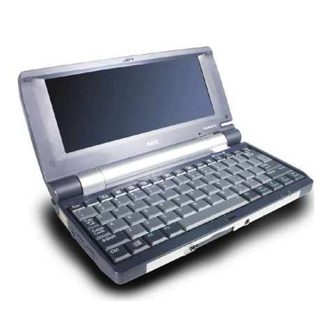
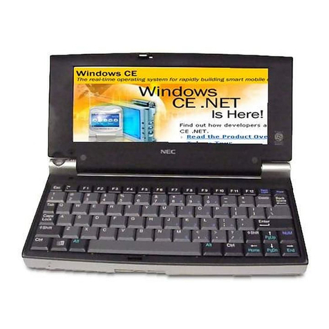
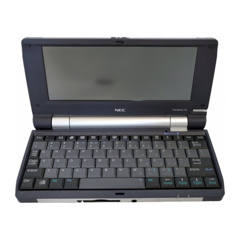
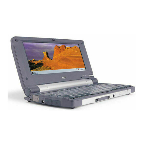
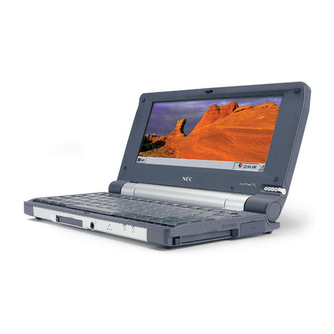
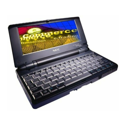
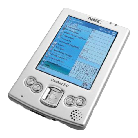
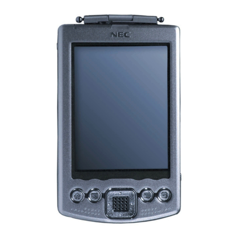
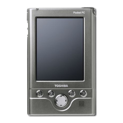
NEC Barracuda User manual

SERVICE MANUAL
SERVICE MANUAL
BARRACUDA
BARRACUDA
BY
BY
:
:
Richard Wang
Richard Wang
TESTING TECHNOLOGY DEPARTMENT / TSSC
MAR. 2002
MAR. 2002

Barracuda PDA Maintenance
1
Contents
1. Hardware Engineering Specification ----------------------------------------------------------------------------
1.1 Overview ----------------------------------------------------------------------------------------------------------------------------
1.2 Main System ------------------------------------------------------------------------------------------------------------------------
1.3 Memory System -------------------------------------------------------------------------------------------------------------------
1.4 Switch Board ----------------------------------------------------------------------------------------------------------------------- 47
1.5 Other Feature ---------------------------------------------------------------------------------------------------------------------- 50
2. System View & Disassembly --------------------------------------------------------------------------------------- 55
2.1 Tool introduction ------------------------------------------------------------------------------------------------------------------ 55
2.2 System View ------------------------------------------------------------------------------------------------------------------------ 56
2.3 System Disassembly --------------------------------------------------------------------------------------------------------------- 59
3. Definition & Location of Connectors / Major Components ------------------------------------------------ 69
3.1 Main Board ( Side A ) ------------------------------------------------------------------------------------------------------------- 69
3.2 Main Board ( Side B ) -------------------------------------------------------------------------------------------------------------
3.3 Switch Board ( Side A,B ) --------------------------------------------------------------------------------------------------------
3.4 Barracuda Memory Board ------------------------------------------------------------------------------------------------------- 71
4. Pin Descriptions of Major Components ------------------------------------------------------------------------- 72
4.1 Intel® StrongARM* SA-1110 Microprocessor -------------------------------------------------------------------------------
5. System Block Diagram ---------------------------------------------------------------------------------------------- 75
6. Barracuda PPC Image Update ------------------------------------------------------------------------------------ 76
6.1 Burning D.M. ------------------------------------------------------------------------------------------------------------------------ 76
6.2 Burn Image -------------------------------------------------------------------------------------------------------------------------- 81
3
3
3
40
70
71
72

Barracuda PDA Maintenance
2
Contents
7. Barracuda Service TPI ---------------------------------------------------------------------------------------------
7.1 Switch Definition -------------------------------------------------------------------------------------------------------------------
7.2 Test Equipment ---------------------------------------------------------------------------------------------------------------------
7.3 Test Program ------------------------------------------------------------------------------------------------------------------------
7.4 Test Flow Chart --------------------------------------------------------------------------------------------------------------------
7.5 Test item -----------------------------------------------------------------------------------------------------------------------------
7.6 D.M. Test Introduction ------------------------------------------------------------------------------------------------------------
8. Trouble Shooting -----------------------------------------------------------------------------------------------------
8.1 No Power ----------------------------------------------------------------------------------------------------------------------------
8.2 LCD No Display or Display Abnormal ----------------------------------------------------------------------------------------
8.3 Memory Test Error ---------------------------------------------------------------------------------------------------------------
8.4 Rocketeer Socket Error ----------------------------------------------------------------------------------------------------------
8.5 Cradle Function Test Error -----------------------------------------------------------------------------------------------------
8.6 Audio Function Failure ----------------------------------------------------------------------------------------------------------
8.7 Touch Screen Function Failure -------------------------------------------------------------------------------------------------
8.8 Switch Board Function Failure -------------------------------------------------------------------------------------------------
9. Spare Parts List ------------------------------------------------------------------------------------------------------
10. System Exploded Views -------------------------------------------------------------------------------------------
11. Circuit Diagram-----------------------------------------------------------------------------------------------------
118
123
127
129
131
133
135
137
139
150
152
87
87
88
88
89
91
98
119
12. Reference Material ------------------------------------------------------------------------------------------------- 177

Barracuda PDA Maintenance
3
1. Hardware Engineering Specification
1.1 Overview
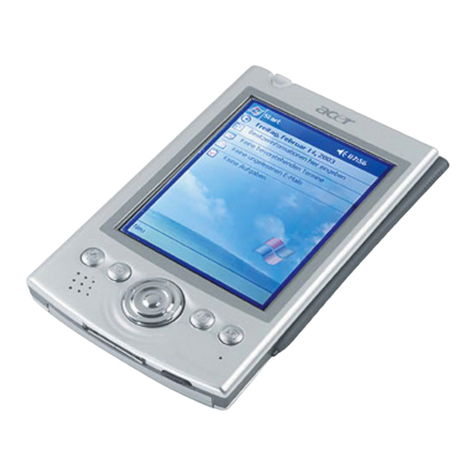
This documents descript the electrical functionality of Barracuda which is an embedded system using Intel SA1110 SOC
& Microsoft Pocket PC operation system “ Merlin Pro “ .
Barracuda is a slim and fashion form-factor with mutimedia capability . It equip with 64K color 320*240 portrait
reflective TFT LCD , touch screen input , one stereo audio out earphone Jack , one microphone and speaker for voice
recording and playback , IrDA , RS232 , USB , Jog wheel and some S/W application hot keys , SD slot , proprietary
extension sled port for versatile expansion capability , a Amber color battery charger LED and a red color Notification
LED .
There are three Boards included in the main system : Main board , memory board , switch board .
1.2 Main system
1.2.1 System Block Diagram

Barracuda PDA Maintenance
4
Block Diagram

Barracuda PDA Maintenance
5
Power Block Diagram

Barracuda PDA Maintenance
6
1.2.2.1 CPU: Intel StrongARM SA1110-206MHz
The SA-1110 is a general-purpose, 32-bit RISC microprocessor with a 16 Kbyte instruction cache, an 8 Kbyte
write-back data cache, a minicache, a write buffer, a read buffer, and a memory management unit (MMU)
combined in a single chip. The SA-1110 is software compatible with the ARM * V4 architecture processor famil
y
and can be used with ARM * support chips such as I/O, memory, and video.
Features of the SA-1110 CPU
High Performance -- 235 Dhrystone 2.1 MIPS @ 206 MHz
Low power (normal mode) -- <400 mW @ 1.75 V/206 MHz
Integrated clock generation
Internal phase-locked loop (PLL)
3.686 MHz oscillator
32.768 KHz oscillator
Power-management features
Normal (full-on) mode
Idle (power-down) mode
Sleep (power-down) mode
Big and little endian operating modes
3.3 V I/O interface
256-pin mini-BGA package (mBGA)
32-way set-associative caches
16 Kbyte instruction cache
8 Kbyte write-back data cach
32-entry memory-management units
Maps 4 Kbyte, 8 Kbyte, or 1 Mbyte
1.2.2 Main Board

Barracuda PDA Maintenance
7
Write buffer
8-entry, between 1 and 16 bytes each
Read buffer
4-entry, 1, 4, or 8 words
Memory bus
Interfaces to ROM, synchronous mask ROM (SMROM), Flash, SRAM, SRAM-like variable latency
I/O, DRAM, and synchronous DRAM (SDRAM)
Supports two PCMCIA sockets
SA-1110 Features

Barracuda PDA Maintenance
8
The SA-1110 consists of the following functional blocks:
• Processing Core
The processor is the ARM * SA-1 core with a 16 Kbyte instruction cache (Icache) and 8 Kbyte data cache
(Dcache). The instruction (I) and data (D) streams are translated through independent
memory-management units (MMUs). Stores are made using a four-line write buffer. The performance of
specialized load routines is enhanced with the four-entry read buffer that can be used to prefetch data for
use at a later time. A 16-entry minicache provides a smaller and logically separate data cache that can be
used to enhance caching performance when dealing with large data structures.
• Memory and PCMCIA Control Module
The memory and PCMCIA control module (MPCM) supports four banks of fast-page-mode (FPM),
extended-data-out (EDO), and/or synchronous DRAM (SDRAM). It also supports up to six banks of static
memory: all six banks allow ROM or Flash memory, each with non-burst or burst read timings.
Additionally, the lower three static banks support SRAM, the upper three static banks support variable
latency I/O devices (with the variable data latency controlled by a shared data ready input), and the lower
four static banks support synchronous mask ROM (SMROM). SMROM is supported only on 32-bit data
busses. All other dynamic and static memory types and variable latency I/O devices are supported on eithe
r
16-bit or 32-bit data busses. Expansion devices are supported through PCMCIA control signals that share
the memory bus data and address lines to complete the card interface. Some external glue logic (buffers and
transceivers) is necessary to implement the interface. Control is provided to permit two card slots with
hot-swap capability.
• Peripheral Control Module
The peripheral control module (PCM) contains a number of serial control devices, an LCD controller as
well as a six-channel DMA controller to provide service to these devices:
An LCD controller with support for passive or active displays
A universal serial bus (USB) endpoint controller
A serial controller with supporting 115 Kbps and 4 Mbps IrDA protocols
A 16550-like UART supporting 230 Kbps
A CODEC interface supporting Motorola SPI,National Microwire, TI Synchronous Serial, or the
Philli
p
s UCB1100 and UCB1200
p
rotocol
Barracuda PDA Maintenance
9
• System Control Module
The system control module (SCM) is also connected to the peripheral bus. It contains five blocks used for
general system functions:
A real-time clock (RTC) clocked from an independent 32.768 kHz oscillator
An operating system timer (OST) for general system timer functions as well as a watchdog mode
Twenty-eight general-purpose I/Os (GPIO)
An interrupt controller
A power-management controller that handles the transitions in and out of sleep and idle modes
A reset controller that handles the various reset sources on the processor
SA-1110 Block Diagram

Barracuda PDA Maintenance
10
SA-1110 Processor LCD controller:
The SA-1110’s LCD controller has three types of displays:
Passive Color Mode….. Supports a total of 375 possible colors, displaying any of 256 colors for each frame.
Active Color Mode……Supports up to 65535 colors (16-bit).
Passive Monochrome Mode … Supports 15 gray-scale levels.
Display size up to 1024 x 1024 pixels are supported. However, the size of encoded pixel data within the frame
buffer limits the maximum size screen the LCD can drive due to memory bus bandwidth.
The LCD controller also supports single- or dual displays. Encoded pixel data is stored in external memorv in a
frame buffer in 4-, 8-, 12-, or 16-bit increments and is loaded into a 5-entry FIFO (32 bits per entry ) on a demand
basis using the LCD’s own dedicated dual-channel DMA controller. One channel is used for single-panel displays
and two are used for dual-panel displays.
Frame buffer data contains encoded pixel values that are used by the LCD controller as pointers to index into a
256-entry x 12-bit wide palette. Monochrome palette entries are 4 bits wide; color palette entries are 12 bits wide.
Encoded pixel data from the frame buffer. which is 4 bits wide, address the top 16 locations of the palette; 8-bit
pixel data accesses any the 256 entries within the palette. When passive color 12-bit pixel mode is enable, the
color pixel values bypass the palette and are fed directly to the LCD’s dither logic. When active color 16-bit pixel
mode is enabled, the pixel value not only bypasses the palette, but also bypasses the dither logic and is sent
directly to the LCD’s data pins.
Once the 4- or 8-bit encoded pixel value to select a palette entry, the value programmed within the entry is
transferred to the dither logic, which uses a patented space- and time- based dithering algorithm to produce
the pixel data that is output to the screen. Dithering causes individual pixels to be turned off on each frame at
varying rates to produce the 15 levels of gray for monochrome screen and 15 levels each for the red, green,
and blue pixel components for color screens, providing a total of 3375 colors (256 colors are available on each
frame). The data output from the dither logic is placed in a 19-entry pin data FIFO before it is placed out on the
LCD’s pins and driven to the display using pixel clock.

Barracuda PDA Maintenance
11
Depending on the type of panel used, the LCD controller is programmed to use either 4-, 8-, or 16-pixel data
output pins. Single –panel monochrome displays use either four or eight data pins to output 4 or 8 pixels for each
pixel clock; single-panel color displays use eight pins to output 2-2/3 pixels each pixel clock ( 8 pins / 3 colors /
pixel = 2-2/3 pixels per clock ). The LCD controller also supports dual-panel mode, which causes the LCD
controller’s data lines to be split into two groups, one to drive the top half and one to drive the bottom half of the
screen. For dual-panel displays, the number of pixel data output pins is doubled, allowing twice as many pixels
to be output each pixel clock to the two halves of the screen.
In active color display mode, the LCD controller can drive TFT displays. The LCD’s line clock pin functions as a
horizontal sync ( HSYNC ) signal, the frame clock pin functions as a vertical sync ( VSYNC ) signal, and the ac
bias pin functions as an output enable ( OE ) signal. In TFT mode, the LCD’s dither logic is bypassed, sending
sending selected palette entries ( 12 bits each ) directly to the LCD’s data output pins. Additionally, 16-bit pixels
can be used that bypass both the palette and the dither logic.
The LCD controller can be configured in active color display mode and used with an external DAC ( and
optionally an external palette ) to drive a video monitor. Note that only monitors that implement the RGB
data format can be used; the LCD controller does not support the NTSC standard .
When the LCD controller is disabled, control of its pins is given to the peripheral pin controller ( PPC ) to
be used as general-purpose digital input/output pins that are noninterruptible. The LCD controller’s pins
include:
LDD 7:0
Data lines used to transmit either four or eight data values at a time to the LCD display. For
monochrome displays, each pin value represents a pixel; for passive color, groupings of three
pin values represent one pixel ( red, green, and blue data values ). In single-panel monochrome
mode, LDD 3:0 pins are used. For double-pixel data, single-panel monochrome, dual-panel
monochrome, single-panel color, and active color modes LDD 7:0 are used.

Barracuda PDA Maintenance
12
GPIO 9:2
when dual-panel color or 16 bit TFT operation is programmed, GPIO pins are used as the additional,
required LCD data lines to output pixel data to the screen.
L_PCLK
Pixel clock used by the LCD display to clock the pixel data into the line shift register. In passive mode.
pixel clock transitions only when valid data is available on the data pins. In active mode, pixel clock
transitions continuously and the ac bias pin is used as an output to signal when data is available on
the LCD’s data pins.
L_LCLK
Line clock used by the LCD display to signal the end of a line of pixels that transfers the line data from
the shift register to the screen and increment the line pointers. Also, it is used by TFT displays as the
horizontal synchronization signal.
L_FCLK
Frame clock used by the LCD displays to signal the start of a new frame of pixels that resets the line
pointers to the top of the screen. Also, it is used by TFT displays as the vertical synchronization sibnal.
L_BIAS
AC bias used to signal the LCD display to switch the polarity of the power supplies to the row and
column axis of the screen to counteract DC offset. In TFT mode, it is used as as the output enable
to signal when data should be latched from the data pins using the pixel clock.
The pixel clock frequency is derived from the output of the on-chip PLL that is used to clock the CPU ( CCLK )
and is programmable from CCLK/6 to CCLK/514. each time new data is supplied to the LCD data pins, the
pixel clock is toggled to latch the data into the LCD display’s serial shifter.

Barracuda PDA Maintenance
13
The line clock toggles after all pixels in a line have been transmitted to the LCD driver and a programmable
number of pixel clock wait states have elapsed both at the beginning and end of each line. In passive mode,
the frame clock is asserted during the first line of the screen. In active mode, the frame clock is asserted
at the beginning of each frame after a programmable number of line clock wait states occur. In passive
display mode, the pixel clock does nit transition when the line clock is asserted. However, in active display
mode, the pixel clock transitions continuously and the ac bias bin used as an output enable to signal when
valid pixels are present on the LCD’s data lines. In passive mode, the ac bias pin can be configured to
transition each time a programmable number of line clocks have elapsed to signal the display to reverse the
polarity of its voltage to counteract DC offset in the screen.
LCD Controller Operation
The LCD controller supports a variety of user-programmable options including display type and size frame
buffer, encoded pixel size, and output data width. Although all programmable combinations are possible,
the selection of displays available within the market dictate which combinations of these programmable
options are practical. The type of external memory system implemented by the user limits the bandwidth
of the LCD’s DMA controller, which, in turn, limits the size and type of screen that can be controlled. The
user must also determine the maximum bandwidth of the SA-1110’s external bus that the LCD is allowed
to use without negatively affecting all other functions that the SA-1110 must perform. Note that the LCD’s
DMA engine has highest priority on the SA-1110’s internal data bus structure ( ARM system bus ) and
can “starve” other masters on the bus, including the CPU.
The following sections describe individual functional blocks within the LCD controller, frame buffer and
palette memory organization, and the LCD’s DMA controller. The sections are arranged in order of data
flow, starting with the off-chip frame buffer and ending with the pins that interface to the LCD display.

Barracuda PDA Maintenance
14
1.2.2.2 UDA1341TS Economy audio CODEC
The UDT1341TS is a single-chip stereo Analog-to-Digital Converter (ADC) and Digital-to-Analog Converter
(DAC) with signal processing features employing bit stream conversion techniques. It's fully integrated analog.
Front end, including Programmable Gain Amplifier (PGA) and a digital Automatic Gain Control (AGC). Digital
Sound Processing (DSP) featuring makes the device an excellent choice for primary home stereo MiNi Disc
applications, but by virtue of its low power and low voltage characteristics it is also suitable for Portable applications
such as MD/CD boom boxes, notebooks PCs and digital video cameras.
The UDA1341TS is similar to the UDA1340M and the UDA1344TS but adds features such as digital mixing of
Two input signals and one channel with a PGA and a digital AGC. The UDA1341TS supports the I2S-
b
us data forma
t
with word lengths of up to 20 bits, the MSB-justified data format.
With word lengths of up to 20 bits, the LSB-justified serial data format with word lengths of 16,18 and 20 bits an
d
three combinations of MSB data output combined with LSB 16,18 and 20 bits data input.
The UDA1341TS has DSP features in playback mode like de-emphasis, volume, bass boots, treble and soft mute.
Which can be controlled via the L3-interface with a micro-controller.
Features:
General
Low power consumption
3.0V power supply
256fs, 384fsor 512fssystem clock frequencies ( fsys )
Small package size ( SSOP28 )
Partially pin compatible with UDA1340M and UDA1344TS
Fully integrated analog front end including digital AGC
ADC plus integrated high-pass filter to cancel DC offset
ADC supports 2V ( RMS value ) input signals
Overload detector for easy record level control
Separate power control for ADC and DAC
Easy application
Functions controllable via L3-interface

Barracuda PDA Maintenance
15
Multiple format data interface
I2S-bus, MSB-justified and LSB-justified format compatible
Three combinational data formats with MSB data output and LSB 16, 18 or 20 bits data input
1fs input and output format data rate
DAC digital sound processing
Digital dB-linear volume control ( low microcontroller load )
Digital tone control, bass boots and treble
Digital de-emphasis for 32, 44.1 or 48 kHz audio sample frequencies ( fs)
Soft mute
Advanced audio configuration
DAC and ADC polarity control
Two channel stereo single-ended input configuration
Microphone input with on-board PGA
Optional differential input configuration for enhanced ADC sound quality
Stereo line output ( under microcontroller volume control )
Digital peak level detection
High linearity, dynamic range and low distortion

Barracuda PDA Maintenance
16
1.2.2.3 Audio Amplifier: NS LM4867
General Description
The LM4867 is a dual bridge-connected audio power amplifier which, when connected to a 5V supply, will
deliver 2.1W to a 4Ωload or 2.4W to a 3Ωload with less than 1.0% THD+N. The LM4867 uses advanced, latest
generation circuitry to eliminate all traces of clicks and pops when the supply voltage is first applied. The
amplifier has a headphone-amplifier-select input pin. It is used to switch the amplifiers from bridge to
single-ended mode for driving headphones. A new circuit topology eliminates headphone output coupling
capacitors. A MUX control pin allows selection between the two sets of stereo input signals. The MUX
control can also be used to select between two different customer-specified closed-loop responses.
Boomer audio power amplifiers are designed specifically to
p
rovide high quality output power from a surface
mount package and require few external components. To simplify audio system design, the LM4867 combines
dual bridge speaker amplifiers and stereo headphone amplifiers in one package.
The LM4867 features an externally controlled power-saving micropower shutdown mode, a stereo
headphone amplifier mode, and thermal shutdown protection.
Features
Advanced “click and pop”suppression circuitry
Eliminates headphone amplifier output coupling capacitors
Stereo headphone amplifier mode
Input mux control and two separate inputs per channel
Thermal shutdown protection circuitry
LLP, TSSOP, and exposed-DAP TSSOP packaging available

Barracuda PDA Maintenance
17
Typical Audio Amplifier Application Circuit

Barracuda PDA Maintenance
18
1.2.2.4 Touch Screen Controller Chip with ADC: Philips semiconductors UCB1300
General Description
The UCB1300 is a single chip, integrated mixed signal audio and telecom codec. The single channel audio codec
is designed for direct connection of a microphone and a speaker. The built-in telecom codec can directly be connecte
d
to a DAA and supports high speed modem protocols. The incorporated analog-to-digital converter and the touch
screen interface provides complete control and read-out of an 4 wire resistive touch screen. The 10 general purpose
I/O pins provide programmable inputs and/or outputs to the system.
The UCB1300 has a serial interface bus (SIB) intended to communicate to the system controller. Both the codec
input data and codec output data and the control register data are multiplexed on this SIB interface.
Features
48 pin LQFP (SOT313-2) small body SMD package and low external component count results in minimal PCB
space
12-bit sigma delta audio codec with programmable sample rate, input and output voltage levels, capable of
connecting directly to speaker and microphone, including digitally controlled mute, loopback and clip
detection functions
14-bit sigma delta telecom codec with programmable sample rate, including digitally controlled in
p
ut voltage
level, mute, loopback and clip detection functions. The telecom codec can be directly connected to a Data
Access Arrangement (DAA) and includes a built in sidetone suppression circuit.
Complete 4 wire resistive touch screen interface circuit supporting position, pressure and plate resistance
Measurements
10-bit successive approximation ADC with internal track and hold circuit and analog multiplexer for touch
screen read-out and monitoring of four external high voltage (7.5V) analog voltages
High speed, 4 wire serial interface data bus (SIB) for communication to the system controller

Barracuda PDA Maintenance
19
3.3V supply voltage and built in power saving modes make the UCB1300 optimal for portable and battery
powered applications
Maximum operating current 25 mA
10 general purpose IO pins
UCB1300 Block Diagram
Table of contents
Other NEC Handheld manuals

NEC
NEC MOBILEPRO 800 - User manual

NEC
NEC MOBILEPRO 800 - Operating manual

NEC
NEC MobilePro 250e User manual

NEC
NEC MOBILEPRO 900C User manual

NEC
NEC MOBILEPRO 900C Instruction Manual

NEC
NEC MOBILEPRO 450H User manual

NEC
NEC MOBILEPRO 780 - User manual

NEC
NEC MOBILEPRO 900 User manual

NEC
NEC MOBILEPRO 750C H User manual

NEC
NEC MOBILEPRO P300 User manual

NEC
NEC MOBILEPRO 900C User manual

NEC
NEC MOBILEPRO 800 - User manual

NEC
NEC S1596-01 User manual

NEC
NEC MOBILEPRO P300 - 2001 User manual

NEC
NEC 700 User manual

NEC
NEC MOBILEPRO 750C - VERSION 1999 User manual

NEC
NEC 700 User manual

NEC
NEC SuperScript 750C User manual

NEC
NEC MOBILEPRO HPC User manual

NEC
NEC MOBILEPRO 900 Instruction Manual