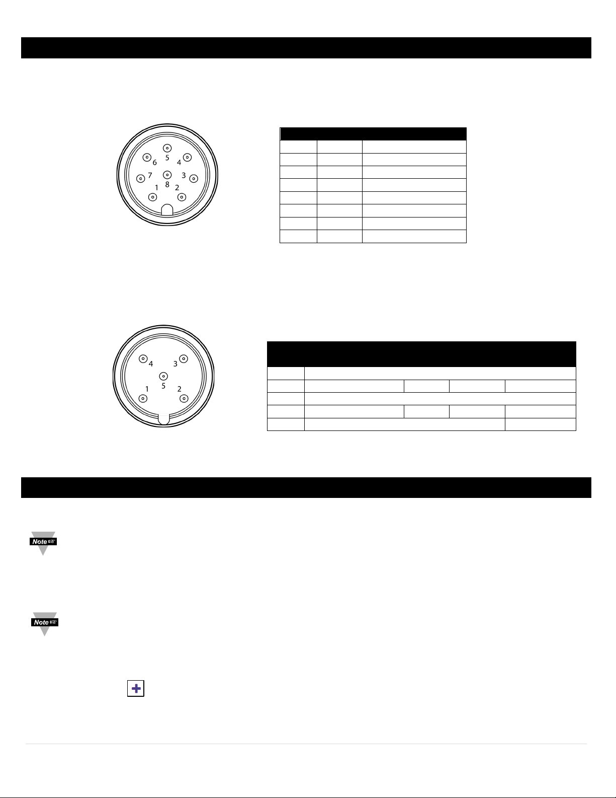
Omega SP-013 User manual

2 | Page
omega.com [email protected]
Servicing North America:
Omega Engineering, Inc.
800 Connecticut Ave. Suite 5N01, Norwalk, CT 06854
Toll-Free: 1-800-826-6342 (USA & Canada only)
Customer Service: 1-800-622-2378 (USA & Canada only)
Engineering Service: 1-800-872-9436 (USA & Canada only)
U.S.A.
Headquarters:
Tel: (203) 359-1660
Fax: (203) 359-7700
The information contained in this document is believed to be correct, but OMEGA accepts no liability for any errors it contai
ns and
reserves the right to alter specifications without notice.

3 | Page
Table of Contents
1Notes, Warnings, and Cautions .................................................................................................................. 5
2Introduction .............................................................................................................................................. 6
3Hardware Setup ........................................................................................................................................ 7
3.1 Connecting your Layer N Smart Interface ..........................................................................................................7
3.2 Digital Input Wiring Diagram ............................................................................................................................7
4SYNC Configuration ................................................................................................................................... 7
4.1 Connecting to SYNC - Automatic Detect ............................................................................................................7
4.2 Connecting to SYNC – Manual...........................................................................................................................7
4.2.1 Communication Interface..................................................................................................................................... 8
4.3 Digital Inputs Interface .....................................................................................................................................9
4.4 Configurable Digital I/O..................................................................................................................................11
4.4.1 Input Settings ..................................................................................................................................................... 11
4.4.2 Output Settings .................................................................................................................................................. 11
4.4.2.1 ON/OFF Functions........................................................................................................................................................... 12
4.4.2.2 Pulse-Width Modulation (PWM) .................................................................................................................................... 12
4.4.3 Setting Alarms .................................................................................................................................................... 12
4.5 ON/OFF Control .............................................................................................................................................13
5Appendix: SP-013 Registers...................................................................................................................... 14
5.1 Digital Descriptor ...........................................................................................................................................14
5.1.1 Digital Measurement Types ............................................................................................................................... 14
5.1.2 Digital Data Type/Format................................................................................................................................... 15
5.1.2.1 Data Type ........................................................................................................................................................................ 15
5.1.2.2 Factory Calibrate............................................................................................................................................................. 15
5.1.2.3 Sensor Writeable ............................................................................................................................................................ 15
5.1.2.4 Smart Sensor................................................................................................................................................................... 15
5.1.3 Digital Configuration .......................................................................................................................................... 15
5.1.3.1 Sensor Range / Type ....................................................................................................................................................... 15
5.1.3.2 Lock ................................................................................................................................................................................. 15
5.1.3.3 Apply Scaling ................................................................................................................................................................... 15
5.1.3.4 Assigned .......................................................................................................................................................................... 16
5.1.3.5 Available.......................................................................................................................................................................... 16
5.1.4 Digital I/O Byte ................................................................................................................................................... 16
5.1.5 IPSO Digital Input Sensor Definition................................................................................................................... 16
5.1.5.1 Sensor Trigger Function .................................................................................................................................................. 17
5.2 Digital Input / Output Descriptor ....................................................................................................................17
5.2.1 DIO Sensor Type ................................................................................................................................................. 17
5.2.2 DIO Data Type/Format ....................................................................................................................................... 17
5.2.2.1 Data Type ........................................................................................................................................................................ 17
5.2.2.2 Factory Calibrate............................................................................................................................................................. 17
5.2.2.3 Sensor Writeable ............................................................................................................................................................ 18
5.2.2.4 Smart Sensor................................................................................................................................................................... 18
5.2.3 DIO Input Configuration ..................................................................................................................................... 18
5.2.3.1 Lock ................................................................................................................................................................................. 18
5.2.3.2 Apply Scaling ................................................................................................................................................................... 18
5.2.3.3 Assigned .......................................................................................................................................................................... 18
5.2.3.4 Available.......................................................................................................................................................................... 18
5.2.4 DIO Device Configuration................................................................................................................................... 18
5.2.4.1 Invert............................................................................................................................................................................... 18
5.2.4.2 Enable ............................................................................................................................................................................. 18

4 | Page
5.2.5 DIO IPSO Definition ............................................................................................................................................ 19
5.2.5.1 Sensor Trigger Function .................................................................................................................................................. 19
5.2.6 DIO Input Circuitry.............................................................................................................................................. 19
5.3 Outputs .........................................................................................................................................................20
5.3.1 PWM Rate........................................................................................................................................................... 20
5.3.2 Active State......................................................................................................................................................... 20
5.3.3 Output Drive....................................................................................................................................................... 20
5.3.4 Output Type........................................................................................................................................................ 20
6Specifications .......................................................................................................................................... 21

5 | Page
1Notes, Warnings, and Cautions
If the equipment is used in a manner not specified in this manual, the protection by the equipment may be impaired.
Do not operate the equipment in flammable or explosive environments.
It is important to read and follow all precautions and instructions in this manual before operating or commissioning this
device as it contains important information relating to safety and EMC. Failure to follow all the safety precautions may
result in injury and / or damage to your equipment.
The following labels identify information that is especially important to note:
Note: Provides you with information that is important to successfully setup and use the SP-013.
Caution or Warning: Tells you about the risk of electrical shock.
Caution, Warning, or Important: Tells you of circumstances that can affect the instruments functionality and must
refer to accompanying documents.

6 | Page
2Introduction
The Layer N SP-013 Digital Interface Smart Probe provides an easy way to integrate digital pulse inputs to your Layer N
Ecosystem. The SP-013 accepts digital pulse inputs through its M12 5-pin connector and Layer N Smart Interfaces through
its M12 8-pin connector. The optional M12.5-S-M-FM connector can be utilized to easily connect wire leads to your SP-013.
The SP-013 may be configured to monitor the on/off state of the input signals, the pulse rate/ duty cycle of the primary
input, or the pulse delay between the two signals. The pulse totalizing function supports both standard counting and
up/down counting.
The Layer N SP-013 features 2 configurable digital I/O pins. These can be used for a myriad of applications including driving
relays, physical alarms, or sensing dry contacts like door switches. The SP-013 can also be utilized as an edge controller, with
autonomous independent decision-making capabilities to generate local alarms or provide control outputs based on sensor
inputs.
Included with your SP-013
•SP-013 Unit
•Quick Start Guide
Additional Material Needed
•Layer N Smart Interface\Computer with Windows OS
•SYNC configuration software
Optional Materials
•M12.5-S-M-FM Screw Terminal Accessory

7 | Page
3Hardware Setup
3.1 Connecting your Layer N Smart Interface
The SP-013 requires a Layer N Smart Interface to connect to your computer. Use the M12 8-Pin Connector diagram below to
connect your SP-013 to your Layer N Smart Interface.
3.2 Digital Input Wiring Diagram
The Layer N SP-013 accepts digital pulse inputs through its M12 5-Pin connector. If you are connecting wire directly to the
SP-013, view the wiring diagrams provided below:
4SYNC Configuration
Layer N Smart Probe products are easily configurable through SYNC configuration software. Ensure SYNC is running on your
Windows OS computer before continuing. Connect your SP-013 to your computer through your Layer N Smart Interface.
Note: SYNC is available to download for free on the OMEGA website.
4.1 Connecting to SYNC - Automatic Detect
Once the SP-013 and Layer N Smart Interface are connected to your computer, SYNC will automatically detect it and begin
displaying digital input readings.
Note: If you have successfully connected your SP-013 to SYNC and have readings appearing in SYNC, skip ahead to
the section 3.3 Digital Input Interface.
4.2 Connecting to SYNC – Manual
If SYNC does not automatically detect your device, follow these instructions to manually connect it.
Step 1: Click on the icon located on the top left of the SYNC interface.
Step 2: Proceed through the Add Device Wizard and click End Device / Probe.
Pin
Name
Function
Pin 1
DIO 0
Discrete I/O Signal 0
Pin 2
INTR
Interrupt Signal
Pin 3
SCL
I2C Clock Signal
Pin 4
SDA
I2C Data Signal
Pin 5
Shield
Shield Ground
Pin 6
DIO 1
Discrete I/O Signal 1
Pin 7
GND
Power Ground
Pin 8
3.3VDD
Power Supply
Pin
Frequency, Width,
Duty Cycle
Delay
Up/Down
Counter
Digital Input
Pin 1
3.3V Power
Pin 2
Pulse
Pulse A
Pulse
Input 1
Pin 3
GND
Pin 4
Enable
Pulse B
Direction
Input 3
Pin 5
Reset
Input 2
M12 8-Pin Connector
M12 5-Pin Connector

8 | Page
4.2.1 Communication Interface
Set the communication parameters for the Layer N Smart Interface that you are connecting.
Note: The connection type and parameters must be accurate for a proper connection to be established. Failure to
accurately setup communication parameters may result in communication errors.
• Connection Type: Select the type of connection you have between your SP-013 and your computer.
• Command Timeout: The maximum time (in milliseconds) for a command to be completed before the command is
aborted.
Note: The default command timeout is 500 milliseconds. It is recommended that this section be left alone to avoid
communication errors.
• Device Address: If your Smart Interface is part of a Network, enter the Network Address here. The default network
address is 1 for most devices. Please refer to the manual of your Smart Interface for more
information.
Note: The default Device Address is 1.
• Device IP or Port: The COM port number that your device is connected to on your computer.
Important: The following parameters should NOT be changed. These settings should NOT be changed unless the
configuration has been done on the interface.
• BaudRate: Controls bits per second
• DataBits: The number of ‘bits’ in each character sent.
• Parity: A means of checking correctness of character by adding an extra ‘bit’ to the character and setting the value
based on all the other bits in the character.
• StopBits: The number of ‘bits’ used to indicate the end of the character.
Once you have completed setting the communication parameters for your device, click Finish.
USB Communication Interface
USB Serial Communication Interface

9 | Page
4.3 Digital Inputs Interface
The SP-013 accepts digital pulse inputs and may be configured to monitor the on/off state of the 3 input signals, the pulse
rate or pulse duty cycle of the primary input, or the pulse delay between two signals. To use these features, follow these
steps:
Step 1: Click the Inputs configuration tab on SYNC and choose the Digital from the Type dropdown.
Step 2: Select the type of digital input in the Device Range/Type drop own in SYNC. The following types are available:
Selection
Measurement
Description
DIN
Digital Input
3-bit Binary Digital Input
RATE
Frequency
Measure the Frequency of Rising or Falling Edges
WIDTH
Pulse Width
Measure the active time of a signal
DUTY
Duty Cycle
Measure the % of active time of a signal
DELAY
Delay Timer
Measure the time between the rising or falling edges of 2 signals
CNT
Up Counter / Totalizer
Counter with Enable and Reset
U/D_CNT
Up/Down Counter / Totalizer
Counter with Direction and Reset
Pin
Frequency, Width,
Duty Cycle
Delay
Up/Down
Counter
Digital Input
Pin 1
3.3V Power
Pin 2
Pulse
Pulse A
Pulse
Input 1
Pin 3
GND
Pin 4
Enable
Pulse B
Direction
Input 3
Pin 5
Reset
Input 2
M12 5-Pin Connector

10 | Page
Each of the three input pins can be independently set to either have an internal 1.5k Pull Up or Pull Down and can be set to
be either Active High or Active Low. Some typical circuits are shown below:

11 | Page
4.4 Configurable Digital I/O
The Layer N SP-013 features 2 configurable digital I/O pins. These can be used for a myriad of applications including driving
relays, physical alarms, or sensing dry contacts like door switches.
4.4.1 Input Settings
To use a pin as an input, make sure it is set to Active Low (default) in the Output Tab in SYNC.
Each pin has an internal pull-up, but in order to save power, the internal pull-up is only active when the unit takes a
reading. Refer to the following table to decode the input state.
Input 1
Input 0
Reading
Inactive
Inactive
0
Inactive
Active
1
Active
Inactive
2
Active
Active
3
4.4.2 Output Settings
To use a pin as an output, configure the outputs setting in the Output Tab and assign the output to an alarm using
SYNC. For more information on how to set an alarm, refer to section 4.4.4 Setting Alarms.
Output options are set in the Output Tab of SYNC. Each output can be configured as either Active High or Active
Low. When configured as Active High the output conducts normally and becomes high impedance when activated.
When
configured as Active Low the Open Drain output is high impedance normally and will conduct when activated. It is
recommended to change the input type to match the output type so that the output state will be correctly
represented in
logs.
Pin
Name
Function
Pin 1
DIO 0
Discrete I/O Signal 0
Pin 2
INTR
Interrupt Signal
Pin 3
SCL
I2C Clock Signal
Pin 4
SDA
I2C Data Signal
Pin 5
Shield
Shield Ground
Pin 6
DIO 1
Discrete I/O Signal 1
Pin 7
GND
Power Ground
Pin 8
3.3VDD
Power Supply
M12 8-Pin Connector

12 | Page
4.4.2.1 ON/OFF Functions
I/O signals can be changed between Active High, Active Low, and inactive.
Option
Value
Description
Active
LOW
When the output is inactive, it is in a high impedance state.
HIGH
When the output is active, it is in a high impedance state.
Value
OFF
Set output inactive
ON
Set output active
4.4.2.2 Pulse-Width Modulation (PWM)
Pulse Width Modulation controls the amount of power given to a device by cycling the on/off phases of a
digital signal. PWM consists of a duty cycle and frequency. The Duty Cycle measures the amount of time a signal is
in the ON state as a percentage. The frequency controls how fast the PWM cycle is repeated. Users can select
between the following settings:
Option
Value
Description
Rate
100 Hz
Signal has constant 100 Hz frequency with 0-100% Duty Cycle
10 Hz
Signal has constant 10 Hz frequency with 0-100% Duty Cycle
1 Hz
Signal has constant 1 Hz frequency with 0-100% Duty Cycle
0.1 Hz
Signal has constant 0.1 Hz frequency with a 0-100% Duty Cycle
Signal Type
Active LOW
When the output is inactive, it is in a low impedance state
Active HIGH
When the active, it is in a high impedance state.
Level
0-100%
Sets the duty cycle from 0-100%
4.4.3 Setting Alarms
Alarms are set by clicking the icon in SYNC on the desired input signal found in the Inputs Configuration Tab. Setup
the threshold and alarm type in the Condition section and then select which output to turn on in the Action section. The
alarm can be set to be latching or non-latching in the Recovery section.

13 | Page
4.5 ON/OFF Control
To configure ON/OFF Control on a device, navigate to the Output Configuration Tab in SYNC and click on the icon
located to the right of the available outputs. Clicking the icon will open Define ON/OFF Control dialog box as seen below.
Choose the input with the active alarm that you would like to control and set your preferred parameters.

14 | Page
5Appendix: SP-013 Registers
The following Appendix provides the registers and list index for the Layer N SP-013 Digital Input Smart Probe. This
information is intended to aid users who will be making configurations and adjustments to their Layer N SP-013 Digital Input
Smart Probe through the Command Line Interface or other custom interfaces.
Smart Probe devices share a common platform architecture that provides extensive monitoring and control capabilities thru
a set of platform generic registers. These registers may be accessed using I2C based commands directly to the Smart Probe
devices or thru a set of Modbus based registers when using Omega Interface devices. Refer to the Smart Sensor Device
Interface manual for further information.
When powered on or after a device reset each Smart Sensor based device will enumerate 1 or more sensor instances which
are described by the device specific Sensor Descriptors which include configuration options, measurement type and units of
measure for the corresponding sensor values. Additional sensor information is provided in sensor specific IPSO object
descriptions which include extended measurement type, precision and tracking of minimum/maximum readings.
Each enumerated Sensor has a Descriptor Base address location and a Sensor IPOS / Configuration structure address
location based on the sensor mix selected.
Sensor
Descriptor Base
IPSO/Configuration
Enumerated Sensor
0
0x0060 (0xf030)
0x08a8 (0xf454)
All Types (DIO, FREQUENCY, WIDTH, DUTY_CYCLE, DELAY or COUNT)
1
0x0068 (0xf034)
0x09a8 (0xf4d4)
DIO (SP-013-1)
2
0x0070 (0xf048)
0x0aa8 (0xf554)
Not Used
3
0x0078 (0xf03c)
0x0ba8 (0xf5d4)
Not Used
5.1 Digital Descriptor
The SP-013 configures the sensors based on the factory device list and user specified list index.
The Sensor Configuration and Sensor Device fields may be written to provide control of the overall function of the channel
and the signal types used.
Offset
Name
Value
Description
0x00
Measurement Type
0x??
DIO, FREQUENCY, WIDTH, DUTY_CYCLE, DELAY or COUNT
0x01
Data Type/Format
0x46
Float, writeable
0x02
Configuration
0x??
Determines channel and Measurement Type
0x03
Sensor Device
0x??
Determines DIO signal types
0x04..0x08
UOMR
“??”
Units of measure
5.1.1 Digital Measurement Types
The Digital interface provides a measurement dependent on the input range/type selected. The units of measure may
be changed by the user.
Sensor Type
Measurement
SI Derived Units
Measurement
0x18
DIN
DIN
DIN (Digital Inputs)
0x19
FREQUENCY (RATE)
Hz
RATE
0x1a
PUSLE WIDTH
msec
PULSE WIDTH
0x1b
DUTY CYCLE
%
DUTY CYCLE
0x1c
PULSE DELAY
msec
DELAY
0x1d
COUNTER
CNT
COUNTER
0x1e
UP / DOWN COUNTER
CNT
UP/DOWN COUNTER

15 | Page
5.1.2 Digital Data Type/Format
Digital Data Type/Format
7
6
5
4
3
2
1
0
Smart
Sensor
Writeable
Factory
Calibrate
Reserved Data Type
0
1
0
0
6 == Floating point
5.1.2.1 Data Type
The 4-bit Data Type field determines the type of data of the specific sensor.
5.1.2.2 Factory Calibrate
No Factory calibration is used on the SP-013.
5.1.2.3 Sensor Writeable
If the Sensor Writeable bit is set the sensor value may be overwritten with a preset value. This capability is useful in
sensors such as up/down counters, where a preset, or possibly a zero value must be written to the sensor value.
5.1.2.4 Smart Sensor
Refer to the Smart Sensor Device Interface documentation.
5.1.3 Digital Configuration
Digital Configuration
7
6
5
4
3
2
1
0
Available
Assigned/
Channel
Apply
Scaling
Lock Sensor Range / Type
0
1
?
?
(see Below)
5.1.3.1 Sensor Range / Type
Value Range / Type Measurement
Type
Units of
Measure
Signals
DIO2 DIO1 DIO0
0x00
DIO
0x18
DIN
INPUT 2
INPUT 1
INPUT 0
0x01
RATE
0x19
Hz
RESET
ENABLE
CLK
0x02
PULSE WIDTH
0x1a
msec
RESET
ENABLE
CLK
0x03
DUTY CYCLE
0x1b
&
RESET
ENABLE
CLK
0x04
DELAY
0x1c
msec
RESET
CLK B
CLK A
0x05
COUNTER
0x1d
CNT
RESET
ENABLE
CLK
0x06
U/D COUNTER
0x1e
CNT
RESET
DIR
CLK
5.1.3.2 Lock
If set, the user specified units of measure string (4-character maximum) will be used in place of the default.
5.1.3.3 Apply Scaling
For more information on Gain and Offset, refer to the Smart Sensor Manual. If set, the user defined Offset and Gain
values will be used to adjust the sensor reading:
Result = (Raw Reading * Gain) + Offset

16 | Page
5.1.3.4 Assigned
The Assigned bit will always read as 0. Refer to the Smart Sensor Device Interface documentation for further
information.
5.1.3.5 Available
The Available bit will always read as 0. Refer to the Smart Sensor Device Interface documentation for further
information.
5.1.4 Digital I/O Byte
For Digital I/O types the Device Byte field determines the signal types for each of the channel bits.
Digital I/O Byte
CHANNEL 0
A
SIG 2 (ENABLE)
SIG 1 (RESET)
SIG 0 (CLOCK)
7
6
5
4
Description
3
2
Description
1
0
Description
1
0
0
0
N.0. SINK (DRY)
0
0
N.0. SINK (DRY)
0
0
N.0. SINK (DRY)
1
0
0
1
N.C. SINK (DRY)
0
1
N.C. SINK (DRY)
0
1
N.C. SINK (DRY)
1
0
1
0
N.O. SOURCE (WET)
1
0
N.O. SOURCE (WET)
1
0
N.O. SOURCE (WET)
1
0
1
1
N.C. SOURCE (WET)
1
1
N.C. SOURCE (WET)
1
1
N.C. SOURCE (WET)
1
1
As Above
0
0
Not Used
1
1
0
1
Not Used
1
1
1
0
Not Used
1
1
1
1
Not Used
5.1.5 IPSO Digital Input Sensor Definition
The IPSO Digital definition provides signal range, measured min/max values, IPSO object type information
Offset
Name
Value
Description
0x00 Sensor Type <table>
Value
Description
3318
Frequency
33005
Pulse Width
33006
Pulse Delay
33007
Duty Cycle
33002
Counter
33003
Up/down Counter
0x02
Precision
0
Provides reading of xxx
0x04
Sensor Trigger
??
See section Sensor Trigger Function
0x08
Min Measured
??
Minimum reading since last reset
0x0c
Max Measured
??
Maximum reading since last reset
0x10
Min Range
-8388607
Minimum reading
0x14
Max Range
+8388607
Maximum reading

17 | Page
5.1.5.1 Sensor Trigger Function
The Sensor Trigger function is used to reset the IPSO min/max values as well as controlling the Calibration process.
Sensor Trigger Function
7
6
5
4
3
2
1
0
0
0
0
0
0
0
0
Reset
Min/Max
15
14
13
12
11
10
9
8
0
0
Calibration
Reset
Calibration
Status
Calibration
Mode
Capture
High
Capture
Low
Calibration
Start
Setting the Reset Min/Max bit to 1 will reset the Min/Max values recorded by the IPSO process.
No User Calibration process is supported on the Digital inputs and all configuration bits should be written as 0.
5.2 Digital Input / Output Descriptor
The DIO Interface provides 2 digital inputs which are hardwired to the Digital outputs. These may be used to detect the
state of external switches (output off) or to monitor the state of the outputs. The DIO Input descriptor is at base addresses
0x0068.
Offset
Name
Value
Description
0x00
Sensor Type
0x18
Digital Type (Bit mapped)
0x01
Data Type/Format
0x46
Configurable, Float type
0x02
Configuration
0x23
Scaling applied, Bits 0 and 1 enabled
0x03
Sensor Device
0x0f
DIN bits enabled / inverted
0x04..0x08
UOMR
“DIN”
Units of measure
5.2.1 DIO Sensor Type
The interface provides a bit mapped input of the 2 digital signal lines.
Sensor Type
SI Derived Units
Measurement
0x18
DIN
Bit mapped digital inputs
5.2.2 DIO Data Type/Format
DIO Data Type
7
6
5
4
3
2
1
0
Smart Sensor
Sensor
Writable
Factory
Calibrate
Reserved Data Type
0
0
0
0
6 == Floating point
Note: Please refer to the Smart Sensor Interface Technical Guide for more information regarding this descriptor.
5.2.2.1 Data Type
The 4-bit Data Type field determines the type of date of the specific sensor.
5.2.2.2 Factory Calibrate
The Factory Calibrate bit is not used for DIO types.

18 | Page
5.2.2.3 Sensor Writeable
If the Sensor Writeable bit is set the sensor value may be overwritten with a preset value. This capability is useful in
sensors such as up/down counters, where a preset, or possibly a zero value must be written to the sensor value.
5.2.2.4 Smart Sensor
Refer to the Smart Sensor Device Interface documentation.
5.2.3 DIO Input Configuration
DIO Input Configuration
7
6
5
4
3
2
1
0
Available Assigned
Apply
Scaling
Lock Sub Channel Selection
0
0
1
?
0x03 == bits 0 and 1
5.2.3.1 Lock
If set, the user specified units of measure string (4-character maximum) will be used in place of the default DIN.
5.2.3.2 Apply Scaling
If set, the user defined Offset and Gain values will be used to adjust the sensor reading. For more information on Gain
and Offset, refer to the Smart Sensor Manual.
Result = (Raw Reading * Gain) + Offset
5.2.3.3 Assigned
The Assigned bit will always read as 0. Refer to the Smart Sensor Device Interface documentation for further
information.
5.2.3.4 Available
The Available bit will always read as 0. Refer to the Smart Sensor Device Interface documentation for further
information.
5.2.4 DIO Device Configuration
The DIO Device Configuration allows enabling each of the 2 input bits and selecting whether the input is active HIGH or
active LOW. If the Invert Bit is set the signal will be Active Low.
DIO Device Configuration
7
6
5
4
3
2
1
0
Reserved
DIN 1
DIN 0
0 0 0 0
ENABLE
INVERT
ENABLE
INVERT
1
1
1
1
5.2.4.1 Invert
If the Invert bit is set the input is active LOW.
5.2.4.2 Enable
If the Enable bit is set the input is enabled.

19 | Page
5.2.5 DIO IPSO Definition
The DIO input IPSO definition provides signal range, measured min/max values, IPSO object type information.
Offset
Name
Value
Description
0x00
Sensor Type
3349
Bit Mapped Digital
0x02
Precision
0
Provides reading of xxx
0x04
Sensor Trigger Function
??
See section Sensor Trigger Function
0x08
Min Measured
??
Minimum reading since last reset
0x0c
Max Measured
??
Maximum reading since last reset
0x10
Min Range
0
Minimum reading
0x14
Max Range
3
Maximum reading
5.2.5.1 Sensor Trigger Function
The Sensor Trigger function is used to reset the IPSO min/max values as well as to control the Calibration process.
Sensor Trigger Function
7
6
5
4
3
2
1
0
0 0 0 0 0 0 0
Reset
Min/Max
15
14
13
12
11
10
9
8
0
0
0
0
0
0
0
0
Setting the Reset Min/Max bit to 1 will reset the Min/Max values recorded by the IPSO process.
No User Calibration process is supported on the DIO inputs and all bits should be written as 0.
5.2.6 DIO Input Circuitry
The DIO input circuitry shares the output circuitry. The internal processor drives the Output Control signal to turn on
the output driver which will force the output LOW. When the state of the DIO input signal is to be read the processor
applies 3.0 VDC to the Input Bias signal and reads the level detected at the Input Sense. If the output is inactive, an
external signal may be used to force the input level LOW. A diode provides protection of external positive voltages,
allowing the Output driver to activate loads greater than the internal 3.3 VDC.

20 | Page
5.3 Outputs
Two output signals are available which may be configured for ON/OFF or PWM outputs through the Output Configuration
registers 0x0124 and 0x0126.
Note: The Output Drive Type (Open Drain, inverting driver) is fixed.
Outputs
7
6
5
4
3
2
1
0
Output Driver
0
Open Drain, Non
inverting Driver
1
Open Drain, Inverting
Driver
3
Open Drain,
Inverting Driver
Active State
LOW
0
HIGH
1
PWM Rate
100 Hz
0
0
10 Hz
0
1
1 Hz
1
0
0.1 Hz
1
1
15
14
13
12
11
10
9
8
Output Type
Null
0
0
0
0
ON/OFF
0
0
0
1
PWM
0
0
1
0
Reserved
x
1
x
x
1
x
x
x
5.3.1 PWM Rate
The SP-013 probe outputs support the following PWM frequencies:
PWM Rate
Name
Description
0 100 Hz
PWM signal has constant 100 Hertz frequency (10
msec repetition rate) with 0 – 100 % duty cycle
1 10 Hz
PWM signal has constant 10 Hertz frequency (100
msec repetition rate) with 0 – 100 % duty cycle
2 1 Hz
PWM signal has constant 1 Hertz frequency (1 second
repetition rate) with 0 – 100 % duty cycle
3 0.1 Hz
PWM signal has constant 0.1 Hertz frequency (10
second repetition rate) with 0 – 100 % duty cycle
5.3.2 Active State
The SP-013 probe outputs may be configured as Active HIGH or Active LOW. When set to 1 (Active HIGH), the output
will be high impedance when active. When set to 0 (Active LOW), the output will be low impedance when active. The
Factory reset value is 0.
5.3.3 Output Drive
The Output Drive is permanently set to 3, indicating that the output is configured as an Open Drain driver, allowing the
DIN signal to override and read back the state of the output signal.
5.3.4 Output Type
The SP-013 probe supports NULL (0), ON/OFF (1) or PWM (2) outputs. When set to NULL the output signal will be left in
a high impedance state. When set to ON/OFF the Rate information has no affect.
Other manuals for SP-013
1
Table of contents
Other Omega Accessories manuals

Omega
Omega ZW-CM User manual

Omega
Omega CDE683 Series User manual

Omega
Omega TQ514 Series User manual

Omega
Omega FP-5070 Series User manual

Omega
Omega OS35 User manual

Omega
Omega FCLTX-100 Series User manual

Omega
Omega OM-EL-WiFi-T-Plus User manual

Omega
Omega OSHFV Series User manual

Omega
Omega zED User manual

Omega
Omega RH-USB User manual

Omega
Omega OS-MINIUSB series User manual

Omega
Omega SS-015-NA User manual

Omega
Omega FMG70B Series User manual

Omega
Omega DMD-476 User manual

Omega
Omega FTB300 Series User manual

Omega
Omega SS-002 User manual

Omega
Omega OS-MINI SERIES User manual

Omega
Omega RG-2501 Series User manual

Omega
Omega HFS-5 User manual

Omega
Omega HTWT SERIES User manual