ORTEC 455 User manual

tiodel 455
Constant Fraction Timing
Single Channel Analyzer
Operating~ and Service Manual
This manual applies to instruments marked
“Rev 13 (on rear panel)
PrinUd in “.S.A.

OkTEC435 COl?STANTFUACTIONTIMI~ SIlQLB%~Eti AI?&YBm
RFIV455-14
October 28,
1-976
Oo
l
cbemetlc 45$-0101-61, changethe valuer of the follouinp pert@8
ChengeDSfrom type lN754A to 219827A.
ChanseR27 from 1969 to 2050.
C@4ngeR28 from 17M~
to
10M.
ch4u* 8185 fror~l780 to 109.~
A
22-pl eepeeiter,nq ;&econnected fros 1%~7 to gtouad if tequllred
in qu&lLty
a+tol
,&@irrg checbout.

STANDARD WARRANTY FOR ORTEC INSTRUMENTS
ORTEC warrants that the items will be delivered free from defects in material or workmansjtip. ORTEC makes no other
warranties, express or implied, and specifically NO WARRANTY OF MERCHANTABILITY OR FITNESS FOR A
PARTICULAR PURPOSE.
ORTEC’s exclusive Liability is limited to repairing or replacing at ORTEC’s option, items found by ORTEC t0 be defective in
workmanship or materials within one year from the date of delivery. ORTEC’s liability on any claim of any kind, including
negligence, loss or damages arising out of, connected with, or from the performance or breach thereof, or from the
manufacture, sale, delivery, resale, repair, or ure of an+ ~item or services covered by this egreem&nt bra purchase order, shall in
no case exceed the price allocable to the item or service furnished or any pert thereof that gives rim to the claim. In the event
ORTEC fails to manufacture or deliver items called for in this agreement or purchase order, ORTEC’! bXCIUSiVe liability and
buyer’s exclusive remedy shall be release of the buyer from the obligation to pay the purchase price. In no event shall ORTEC
be liable for special or consequential damages.
QUALITY CONTROL
Before being approved for shipment, each ORTEC instrument must pass a stringent set bf~quelity control tests designed to
expose any flaws in materials or workmanship. Permanent records of these tests are maintained for use in warranty repair and
es a source of statistical information for design improvements.
REPAIR SERVICE
If it becomes necessary to return this instrument for repair, it is essential that Customei Servi 2+ be contacted in advance of
its return so that a Return Authorization Number can be assigned to the unit. Also, ORTE must be informed, either in
writing or b$ telephone [(615) 482-441 t] , Of the nature of the fault of the instrument pei+tS retqr.ryd and of the model,
serial, and revision (“Rev” on rear panel) numbers. Failure to do so inay cause unnaces~ary dp!dps,i,n getting the unit repaired..
The ORTEC standard procedure requires that instruments returned for repair pass the sam?;&iility control tests that are used
for new-production instruments. Instruments that are returned should be packed so that they will withstand normal transit
handling and must be shipped PREPAID via Air Parcel Post or United Parcel Service to the nearest ORTEC repair center. The
address label and the package should include the Return Authorization Number assigned. Instruments being returned that are
damaged in transit due to inadequate packing will be repaired et the sender’s expense. and it will be the sender’s responsibility
to make claim with the shipper. Instruments not in warranty will be repaired et the standard charge unless they have been
grossly misused or mishandled, in which case the user will be notified prior to the repair being done.,A quotation will be sent
with the notification.
DAMAGE IN TRANSIT
Shipments should be examined immediately upon receipt for evidence of external or concealed damage. The carrier making
delivery should be notified immediately of any such damage, since the carrier is norm& liable for damage in shipment.
Packing materials, waybills, and other such documentation should be preserved in order to establish claims. After such
notification to the carrier, please notify ORTEC of the circumstances so that assistance can be provided in making damage
claims and in providing replacement equipment if necessary.

iii
TABLE OF CONTENTS
WARRANTY
PHOTOGRAPHS
1. DESCRIPTION
2. SPECIFICATIONS
3. INSTALLATION
3.1 General
3.2 Connection to Power
3.3 Connection to a Linear Amplifier
3.4 Linear Output Signal Connections and Terminating Impedance Considerations
4. OPERATING INSTRUCTIONS 5
4.1 Introduction to Fast Timing with Linear Signals 5
4.2 TYpical Operating Conditions 5
4.3 Front-Panel Control Functions 5
4.4 Rear-Panel Control Functions 6
4.5 Connector Data 6
5. CIRCUIT DESCRIPTION
5.1 Input Circuit
5.2 Single Channel Analyzer
5.3 Reference Levels
5.4 Internal Timing Signal
5.5 Single Channel Output
5.6 External Strobe Operation
7
6. MAINTENANCE
6.1 Testing Performance
6.2 Calibration Adjustments
6.3 Testing the 455 Timing Walk
6.4 Procedure for Adjusting Walk
6.5 Factory Repair
9
9
9
10
10
11
BLOCK DIAGRAM AND SCHEMATIC 455.0101.81 455.0101.Sl
LIST OF FIGURES
Fig. 1.1. Time Resolution as a Function of Dynamic Range
Fig. 4.1. Principle of Constant Fraction Timing Signal Derivation
Fig. 6.1. Basic Interconnections for Level Calibrationr
Fig. 6.2. System Interconnections for 455 Walk Test
Fig. 6.3. Waveforms for Propar Adjustment
Fig. 6.4. Waveforms for Improper Adjustment
ii
iv
1
2
Page
1
5
9
10
10
10

I”
/I 1;
OUTPUT
I
-INPUT ;
I

1
ORTEC 455 CONSTANT FRACTION TIMING SCA
1. DESCRIPTION
The ORTEC 455 Constant Fraction Timing Single Channel
Analyzer provides both pulse-height and timing analysis for
unipolar and bipolar signals. The Constant Fraction Timing
technique providesunexcelled timing on unipolar pulsesand
a unique crossover discriminator shows results better than
heretofore possible with conventional leading edge or cross-
wer discriminators.
Actual timing results obtained with the 455 and fast
plastic scintillators are shown in Figure l-1. The advantage
of the constant fraction timing technique is readily apparent.
With SCA’s which utilize leading edge timing, the risetime
of the input pulses causes degradation of time resolution
because the pulses have varying amplitudes. Constant
Fraction timing compensates for varying amplitudes and
essentially eliminates this timing shift, giving consistently
better timing results. For a 10% fraction, the output occurs
soon after the peak of the input to facilitate gating and
accumulation of dataatvery high input rates. This technique
also minimizes timing shift and dead time when used with
sodium iodide, silicon, and germanium detectors, thereby
allowing better system time resolution and higher counting
rates. Timing results paralleling those in Figure l-l are also
possible with these detectors. The Constant Fraction
technique makes it possible to realize significant improve-
ments in most applications where analysis is made of the
main amplifier output. It allows optimization of time
resolution and extension of dynamic range for neutron-
gamma discrimination.
The 455 can Bccuratelv analyze the o”tput pulses of any
shaping amplifier because the discriminator levels are ex-
tremely sharp and stable. A front-panel control selects four
SCA modes: integral, 100%. 20%. and normal. These modes
of operation are described in the specifications that follow.
With all of its versatility, ease of operation is an intrinsic
quality of the 455. ln:all operating modes and with input
pulse shaping from 0.1 to 10 wc, no risetime compensation
or other adjustments are necessary for proper operation.
The dc-coupled input ‘of the 455 makes it possible to take
full advantage of the baseline restoration of the main
amplifier. For amplifiers with ac-coupled outputs. two
ranges of dc restoration are available. These features ensure
stable discrimination levels for widely varying input count-
ing rates, and hence better energy discrimination.
The continuously adjustable output delay (two ranges
covering 0.1 to 11 ~sec) makes it possible to align output
signals which have actual time differences without a need
for additional delay devices or modules.
-
1.
1 to 100
Figure l-l. Time Resolution as a Function of Dynamic Range

2
2; SPECIFICATIONS
PEflFOR,MANCE
Time shift VI pulse height (walk)
Constant Fraction Timing M&a
FRACTION A front panel switch selects the fraction of
0.1, 0.2, 0.3, 0.4, and 0.5 for Constant Fraction timing
with unipolar or bipolar inputs, or Ei for zero crossing
timing with bipolar inputs.
Walk Ins& Dynamic
System A System 8 Range
<*1.5 Gil.5 1O:l
Qf3.7 <i8 EdI:1
Gf4.5 <*lo 1OO:l
System A: Using ORTEC 410 Amplifier,
single delay line, mode. integrate
GO.1 wag: with delay lines of 0.2 to
z/J=
System 6. Using ORTEC 4w or 451
Amplifier unipolar output with 0.5
waec shaping time and 0.4 fraction.
Walk
Insed
<*1
Bi Mode
Dynamic
Range
1O:l
< f 2.5 50:1 .
<f3 1OO:l
Using ORTEC 410 Amplifier, double
delay line mode, integrate < 0.1, @ec
with delay lines of 0.2 to 2 /Jsec.
Pulse pair resolution O.B!.~sec plus the delay time.
Nonlinearity Lower level 6 f 0.25%. upper level C; f 0.25%.
(Nonlinearity, specifications are limited by the lo-turn
potentiometer.) 5
Temperature stability
upper level: <f O.O05%PC
Lower level : < f 0.005%/Y
Delay: < f O.Ol%pC
CONTROLS
LOWER LEVEL lo-turn control sets the lower level from
100 mV to 10 V (1MH) divisions = 10 V).
UPPER LEVEL IO-turn control sets the upper level from
100mVto10V(1000divisions=lOV).
DELAY RANGE Rear-panel switch selects range of 0.1 to
1.l or 1 .O to 11 pet delay.
DELAY 10.turn control for continuously adjusting output
delay over selected delay range. In the external strobe
mode the delay control adjusts the automatic reset time
from - 5 to 50 mc.
SCA MODES Front panel switch selects the following
modes:
INTEGRAL Timing outputs ocwr for all signals with
amplitudes abwe thelower-level discriminator setting.
NORMAL Timing outputs o&r for signals with ampli-
tudes between the lower-level and upper-level settings.
The MO controls are independently adju$table.
.:$
20% WINDOW Timing outputs occu&!r signals with
amplitudes between the lower level and the sum of
the lower-level and 0.2X upper level. The spa” (1000
-divisions) of the upper-level control (window) is 2 V.
100% WINDOW Timing outputs occur for signals with
amplitudes between the lower level and the sum of
the lower level and the upper level. The span (1000
divisions) of the upper-level control (window) is 0 to
1ov.
RESTORER A 5position rear-panel switch to allow input
dc-coupling. or a high or low baseline restoration rate.
EXT. STROBE/INT/EXT BASELINE A rear-panel switch
selects internal strobe and baseline, external baseline
r@fennce, or external strobe. In the external baseline
mode’ue lo&r level is set by the external reference.
In the exte&i&strobe mdde the timing outputs occur
in coincidence with thestiobepulse..
“. ,,
WALK ADJUST Front panel screwdriver adjust&nt’f3i
precise setting of walk compensation.
CONNECTORS All signal connectors are BNC connectors
(UG-1094/U).
INPUTS
Analog Input
Amplitude range 0 to 10 V
Pulse width range 0.2 to 20 ~.tsec at half amplitude
Polarity Positive (unipolar) or positive portion leading
(bipolar)
Input impedance 1000 ohms dc-coupled

3
External Input -Strobe/Baseline
Input impedance Greaterthan 1000 ohms dc-coupled
Strobe input +2 V niin, +12 V max. 75 nsec min
width
Baseline amplitude 0 to -10 V
OUTPUTS
Timing Outputs. In the Constant Fraction mode the
timing outputs occur when the input pulse has fallen
from its peak by the selected fraction (plus the delay
time). In the Eii (bipolar) mode the timing outputs
occur when the input pulse crosses the baseline
1 (plus the delay time).
NE&the current
output
produces 0.7 V minimum into
5O‘;ghms with r&time < 5 nsec and width < 20 nsec
(front panel).
POS Positive 5 V risetime less than 20 “sec. width
O.~/.WC. &, =< 10 ohms (front panel).
Diroriminator Outputs Thesignal occurs promptly when the
input exceeds the discriminator threshold.
UL Positive5 V,risetime <20 nsec, width 0.5 /.wc, Z. =
< 10 ohms (rear panel).
LL Positive 5 V. risetime < 20 nsec, width 0.5 &wc, Z, =
< 10 ohms (rear panel).
ORDERING INFORMATION
Power Required +24 V 70 mA +12 V 150 mA
-24V59mA -12VlOOmA
Weight (Shipping) 3 lb 6 oz (1.5 kg)
Weight (Net) 2 lb 7 02 (1.1 kg)
Dimensions Standard single width module per TID-20693
mev.)
?i

4
3. INSTALLATION
3.1 General
The ORTEC 455 is designed for installation in an ORTEC
401A/402A Bin and Power Supply, which is intended for
rack mounting. Any vacuum tube equipment operated
in thesame rack must be cooled by circulating air to prevent
any localized heating of the all-transistor circuitry used
throughout the 455. The temperature of equipment
mounted in racks can easily exceed the recommended
maximum of 120°F (50°C) unless precautions are taken.
3.2 Connection to Power
The 455 contains no internal power supply and so must
obtain power from a Nuclear Standard Bin and Power
Supply such as the ORTEC 401A/402A. Turn off the Bin
power supply before inserting or removing modules. The
ORTEC 400 Series modules are designed so that it is not
possible to overload the Bin power supply with a full
complement of modules in the Bin. Since this may not be
true, however, when the Bin contains modules other than
those of ORTEC design, check the power supply voltages
after inserting modules. The 401A/402A has test points on
the power supply control panel to monitor the dc voltages.
3.3 Connection to a Linear Amplifier
The input to the 455 is a front-panel BNC connector. It
may be used to accept outputs from all linear amplifiers
capable of producing 10-V unipolar or bipolar (positive
lobe leading) signals. onto a 1000.ohm load. The input
operating range is from 100 mV to 10 V. If the amplifier
output is attenuated so that it cannot exceed 10 V, the 455
may be used with vacuum tube amplifiers which are capable
of dutput signals to 100 V. Simple resisitve attenuators
installed in the vacuum tube amplifiers will make them
compatible with related transistor equipment.
3.4 Linear Output Signal Connections and Terminating
Impedance Considerations
The source impedance of the 0. to 10-V standard linear
outputs of most ORTEC 400 Series modules is approxi-
mately 1 ohm. Interconnection of linear signals is thus
not critical since the input impedance of the 455 is high and
is’not important in determining the actual signal span,
0 to 10 V, delivered into it. It is permissible to parallel
several loads on a single output while preserving the 0- to
10-V signal span.
Short lengths of interconnecting cable (up to approxi-
mately 4 ft) need not be terminated. If, however, a linear
signal is to pass through more than approximately 4 ft
of cable, it should be terminated in a resistive load equal to
the cable impedance. Since the output impedance is not
purely resistive and is slightly different for each individual
module, coaxial cable of more than 4 ft not terminated
in the characteristic cable impedance will generally cau?e
oscillations. These oscillations can be suppressed for any
length of cable by terminating the cable properly. either in
series at the sending end or in shunt at the receiving end of
the line.
To terminate a cable properly at the receiving end, it may
be necessary to choose an additional parallel resistance
to the input resistance of the driven circuit to make the
combination produce the desired termination resistance.
Series terminating the cable at the sending end may be
preferable when receiving-end terminating is not possible
or desirable. Many ORTEC linear instruments include an
alternate output connector for an output impedance of
93 ohms, and this connector may be used when 93.ohm
cable is used for the int&onnection: the impedance
match will then be complete without any compensation
at the high-impedance receiving end. When series terminat-
ing at the sending end, full signal span (amplitude) is
obtained at the receiving end, only when it is essentially
unloaded or is loaded with an impedance many times that of
the cable. Since the input impedance of the 455 is 1000
ohms, a series termination at the sending end of the cable
will normally provide satisfactory results.
BNC tee connectors and connectors with internal resistive
terminators are available from a number of manufacturers
in nominal values of 50, 100, and 1000 ohms to facilitate
shunt termination at the receiving end of a cable. ORTEC
stocks in limited quantity the following connector ac-
cessories for this application:
ORTEC C-27 loo-ohm Resistive Terminator
O,RTEC C-28 50.ohm Resistive Terminator
ORTEC C-29 BNC Tee Connector

5
4. OPERATING INSTRUCTIONS
4.1 introduction to Fast Timing with Linear Signals
The precise determination of the time of a nuclear event,
simultaneous with the mea~uramant of its energy, hasbeen
restricted in the past to two timing techniques - zero
crossing and level discrimination. In the zero-crossing
method the timing SCA simply detects the time at which
a bipolar linear signal crosses the baseline. For a double-
delay-line shaped signal the zero-crossing phase point con-
tains the same information as the 50% charge collection
time on the leading edge of the signal. For some signals the
zero-crossing point provides excellent time resolution.
There are two rather savera limitations to~the zero-crossing
technique. First, the amplitude n&e of a bipolar signal is
normally worse than a similarly shaped unipolar signal.
Consequently, the edges of the energy window set by the
SCA are not as precise as they would be for a unipolar signal.
The second limitation of the zero-crossing technique is
that the time information cannot be obtained until the
signal crosses the baseline. The added time delay before
getting the time information is not a savera limitation in
DDL applications, but for simulated Gaussian-shaped signals
the added delay may be several microseconds.
A simple level discriminator is used to obtain time infor-
mation by the second technique. The usual mode of
operation allows the level discriminator to trigger on the
leading edge of the signal and to then reset when the signal
falls below the discrimi,nator level. Either of these trigger
points can be used for the timing information. If the
leadingedge trigger point is used, it must be delayed beyond
the peak of the input signal for the single-channel ampli-
tude decision to bemade. The basic limitation of this system
is that it introduces a time walk due to changing signal
amplitudes, and the magnitude of the walk is usuallyequal
to approximately the rise time of the signal. For different
types of signals this walk will range from tens of nano-
seconds to microseconds.
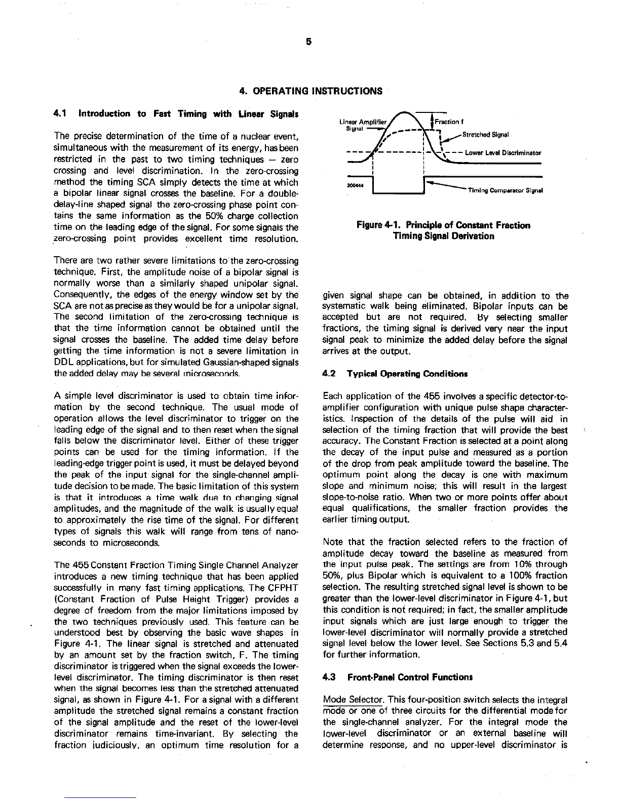
The 455Constant Fraction Timing Single Channel Analyzer
introduces a new timing technique that has been applied
successfully in many fast timing applications. The CFPHT
(Constant Fraction of Pulse Height Trigger) provides a
degree of freedom from the major limitations imposed by
the two techniques previously used. This feature can be
understood best by observing the basic wave shapes in
Figure 4-1. The linear signal is stretched and attenuated
by an amount set by the fraction switch, F. The timing
discriminator is triggered when the signal exceeds the lower-
level discriminator. The timing discriminator is then rasat
when the signal becomes less than the stretched attenuated
signal, as shown in Figure 4-1. For a signal with a different
amplitude the stretched signal remains a cowsent fraction
of the signal amplitude and the re%et of the lower-level
discriminator remains timeinvariant. By selecting the
fraction judiciously, en optimum time rasolution for a
Figure 41. Principle of Constant Fraction
Timing Signal Derivation
given signal shape can be obtained, in addition to the
systematic walk being eliminated. Bipolar inputs can be
accepted but era not required. By selecting smaller
fractions, the timing signal is derived very near the input
signal peak to minimize the added~delay before the signal
arrives at the output.
4.2 Typical Operating Conditions
Each application of the 455 involves a specific datector-to-
amplifier configuration with unique pulse shape character-
istics. inspection of the details of the pulse will aid in
Selection of the timing fraction that will provide the best
accuracy. The Constant Fraction is selected at a point along
the decay of the input pulse and measured as a portion
of the drop from peak amplitude toward the baseline. The
optimum point along the decay is one with maximum
slope and minimum noise; this will rasult in the largest
slope-to-noise ratio. When two or more points offer~about
equal qualifications, the smaller fraction provides the
earlier timing output.
Note that the fraction selected refers to the fraction of
amplitude decay toward the baseline as measured from
the input pulse peak. The settings are from 10% through
50%. plus Bipolar which is equivalent to a 100% fraction
selection. The resulting stretched signal level is shown to be
greater than the lower-level discriminator in Figure 4-1, but
this condition is not required; in fact, the smaller amplitude
input signals which are just large enough to trigger the
lower-level discriminator will normally provide a stretched
signal level below the lower level. See Sections 5.3 and 5.4
for further information.
4.3 Front-Panel Control Functions
Mode Selector. This four-position switch ?elects the integral
mode or one of three circuits for the differential modefor
the single-channel analyzer. For the integral mode the
lower-level discriminator or an external baseline will
determine response, and no upper-level discriminator is

6
involved. For NORM, both discriminators are effective
and their control ranges are completely independent; the
Upper Level control must select a level greater than the
glower Level control or external baseline input. or no
output can be generated. For the 20% WIN position, the
Upper Level control selects the amount by which the
Upper-level discriminator reference exceeds the lower-
level reference. and the control range is 0 to 2 V. For the
100% WIN position the same type of window circuit is
effective, and the Upper Level control range is increased to
the full O-to 10-V dynamic range.
FRACTION. This six-position contrc+is concentric with the
mode selector. It permits selection of lo%, 20%. 30%.
40%. or 50% Fraction for timing or Bi, which is the con-
ventional zero-crossing timing mode. See Sections 4.2,5.3.
and 5.4 for suuggestions on the use of this switch.
UPPER LEVEL. This IO-turn precision potentiometer
selects the upper-level reference. Its range is 0 to 10 V, read
directly by the 1000 divisions of the duo-dial. Whtin the 455
operates in its 20% Window mode, the effective range of
the Upper Level control is 0 to 2 V.
LOWER LEVEL. This IO-turn precision potentiometer
selects the lower-level reference, except when a
rear-panel
switch selects External Baseline. Its range is 0.1 to 10 V.
read directly on the control.
DELAY. This IO-turn precision potentiometer adjusts
fhee from the timing comparator signal to the SCA
output signals, except when a rear-panel switch is set at
External Strobe. The delay can be adjusted from 0.1
through 11 JIS; a rear-panel switch selects either an
0.1. to 1.1./JS range or a 1.0. to 1 I-/IS rangeand the selected
delay is read directly on the control of the potentiom-
eter.
WALK ADJ. This screwdriver potentiometer adjusts for
minimum time walk, as a fine control for any selected
fraction. See Section 6.7 for further information.
4.4 Rear-Panel Control Functions
EXT STROBE/INT/EXT EL. This 3position slide switch
permits the adjacent~ BNC connector to be used for either
of two externally controlled functions. When it is set at
INT, neither of the external functions will be effective.
When it is ~set at EXT STROBE, the SCA timing outputs
occur in coincidence with an external strobe input pulse
furnished thrwgh the BNC, and this must occur within less
than 50 .us after the lower-level discriminator is triggered;
the lower-level reference is set by the front-panel Lower
Level controL during the external strobe mode. When the
switch is set at EXT BL, the front-panel Lower Level
control is disconnected and the lower-level reference must
be furnished by a 0- to negative 10-V bias through the ad-
jacent BNC; internal strobe must be used. since there is no
provision for an external strobe input.
DELAY. This slide switch selects either of the two
Bffective ranges for the Delay front-panel control. The
ranges are 0.1 through 1.1 p and 1.0 through 11 /IS.
BLR. This 3.position slide switch selects the input circuit
appropriate to each specific application. The DC position
his a dc-coupled input and may be used when there is no
baseline offset furnished from the input pulse source. LO
and HI positions refer to the average .input pulse rate; the
LO position selects a passive r&oration circuit, while the
HI position selects an active baseline restorer.
4.5 Connector Data
INPUT. A BNC connector accepts the analog input signals
into input impedance of 1,000 ohms. The input circuit
will be either dc- or ‘ac-coupled; depending upon the
selection of the rear-panel BLR switch. Either positive
unipolar pulses or bipolar pulses with positive leading
portion may be furnished within the O- to +10-V linear
range.
NEG. OUT. A standard ORTEC land NlMl fast negative
logic signal is available through this BNC connector for
optimum timing resolution. This is a current output pulse
that produces 0.7 V minimum into 50 ohms.
POS. OUT. A standard ORTEC land NIM) slow positive
logic signal is available through ‘this BNC connector
for applications such as analyzer gating and coincidence
timing.
UL. A standard ORTEC land NIM) slow positive logic
r&J is furnished through this BNC connector each time
the upper-level discriminator is triggered, without regard
to the internal use of the upper-level, response.
LL. A standard ORTEC land NIMI slow positive logic
*aI is furnished through this BNC connector each time
the lower-level discriminator is triggered, without regard
to the internal use of the lower-level response.
EXT INPUT. This BNC connector accepts either external
strobe pulses or 8” external baseline bias level. depending
upon the selection of the adjacent 3.position slide switch.
Test Points. Oscilloscope test point?. for monitori@ the
input and the two single-channel outputs on the front panel
are availableat each connector. Each test point is connected
to its respective connector through a 470.ohm series
resistor.

7
5. CIRCUIT DESCRIPTION
5.1 Input Circuit
The input signal is presented to a dorestorer circuit, or is
dc-coupled, directly info a unity gain amplifier, Q5 to Q9.
A rear-panel switch selects either HI or LO dc-restoration
rate or de-coupling. Input capacitor Cl i%simply bypassed
for dc-coupling. For the LO restoration rate, Ql and Q2
form a Robinson type of restorer circuit. For the HI
restoration rate, Q3 and Q4 operate as a high-gain dif-
ferential amplifier to feed back a voltage to the emitter of
02 that is inversely proportional to the dc offset voltage
at Cl. Thus, in the HI rate circuit, restoration of thevoltage
to zero is achieved~ by an active closed-loop feedback
amplifier.
Following the restorer. the signal is attenuated for half of
its input value, using resistors R9 and RlO. It is then buf-
fered by the unity gain amplifier, Q5 - Q9, and furnished
to four internal circujts. The amplifier is dc-coupled with a
.very low output impedance to drive all three comparators,
IC 5 through IC 7. with no appreciable loading effectsdue
to the comparator base currents. The signal et the unity
gain amplifier output has half of the input amplitude for its
positive polarity; any negative polarity included in the
input is clipped two diode junctions (approximately -1.4 VI
below zero. The quiescent voltage et the amplifier output is
zero volts.
The amplifier output signal is presented to three voltage
comparators, IC 5. IC 6, and IC
7.
and to a pulse stretcher,
Q17 through Q21. Comparators IC 5 and JC 6 form a con-
ventional single-channel pulse-height analyzer. Comparator
IC 7 and the stretcher perform a unique timing analysis.
5.2
Single Channel Analyzer
Lower Level comparator IC 6 accepts a bias level 6 from
IC 8B and the unity gein amplifier output. In the
quiescent state, IC 6 output is z +1.5 V. When the signal
level exceeds the reference level B, the output switches
rapidly to - -0.5 V and remains until the signal level drops
below the reference level again. The comparator is a type
~A710 with fast switching speed, and responds to signals
as short es 200 ns. The negative transition of the output
triggers two monostables; one forms a Lower Level output
pulse through the rear-panel LL connector and the other is
e temporary memory, to hold the response until an output
trigger occurs.
Upper Level comparator IC 5 accepts a bias level A from
IC 8A and the output from the unity gain amplifier. Its
operation is identical to that of IC 6, discussed above, and
this comparator also triggers two monostabl,~; one forms
an Upper Level output pulse and the other is a temporary
memory.
The Lower Level output pulse is a NIM standard slow
positive pulse formed when IC 46 and Q32 and Q33. a
monostable, receives the negative transistion of the IC 6
comparator output. The output pulse duration is 0.5 p
and its amplitude is +5 V approximately. The pulse occurs
on the leading edge of the input pulse when the input
exceeds the Lower Level bias and is available through the -
rear-panel LL connector.
The Upper Level output pulse is identical to the Lower
Level output discussed above and is generated by IC 4A.
Q40, and Q41. It occurs on the leading edge of the input
pulse when the input exceeds the Upper Level bias and is
available through the rear-panel UL connector.
The temporary memory for the Lower Level comparator
is IC 2, sections A, 6, C, and D. It is a monostable with e
duration of 50 flus but is normally re?et prior to this time,
just after the pulse-height decision is made. Its output
goes from +1.5 V to -0.5 V and is furnished es one of two
inputs to IC 1D. The temporary memory for the Upper Level
comparator is IC 1, sections A, B, end C. It also has a dura-
tion of 50 us, subject to prior reset. The output from this
memory, furnished as the second input to IC 1D. goes from
-0.5 V to +1.5 V when it is triggered.
When either input (or both) to OR gate IC 1D is et +1.5 V,
it will drive Q67 into saturation, thus preventing the timing
signal from appearing at the collector of Q38. A single-
channel output pulse will be generated by e delay mono-
stable, Q45 to Q49, when it recovers after being triggered
by a pulse through Q38; but Q67 must be cut off to
permit the trigger pulse to reach the monostable. Only
when both IC 1D gate inputs are at the low state I- 0 VI
will the trigger pulse be effective. This condition is
equivalent to the logic that permits the generation of e
single-channel output pulse and allows the timing circuit
to determine when the pulse will be generated. The sig
nal into IC ID from IC 1A. B, and C is low when
the Upper Level discriminator has not been triggered or when
the front-panel selector switch is set for Integral mode
operation. The signal into IC 1D from IC 2 is low
only after the Lower Level discriminator has been trig-
gered. Thus, for the Integral mode of operation, e single-
channel output will be generated for each pulse that has an
amplitude greater than the setting of the Lower Level bias
B. For Normal and Window modes e single-channel output
will be generated if the input pulse amplitude exceeds the
B reference level but does not exceed the A reference level
(Upper Level). For each such ,input pulse with too large an
amplitude, a permissive condition will exist for e short
time interval during the input pulse rise time, but the out-
put trigger. will not occur until a selected time after the
input pulsepesk;so the false indication will not be sampled.
5.3
Reference Levels
A 3.bosition rear-panel switch selects External Strobe with
internal baseline control. External Baseline control with
internal strobe, or Internal strobe and baseline. The BL
switch position selects external baseline control. which re-
move-s the Lower Level control from the 455 internal cir-

8
cuit and allows a 0- to -10-V signal to be accepted through
the rear-panel BNC connector for “se as the B reference
level after attenuation by a factor of 2. For either of the
other two switch positions, reference level B is determined
by the setting of the front-panel Lower Level control.
The Lower and Upper Level channels have a common -5-V
reference level, regulated by DE. Lower Level adjustment
R39 selects a level between 0 and -5 V and applies it to
unity gain amplifier Q56, Q59, Q60, Q61, and Q65. The
unity gainamplifier hasa high input impedance for minimum
current drain from the DE reference source and for buffering
the potentiometer from all other circuitry. Upper Level
adjustment R29 independently Selects a level between 0 and
-5 V and applies it to its unity gain amplifier, 054 through
Q57 and Q67.
Following the unity gain amplifiers is the dual operational
amplifier IC 8. The unity gain amplifier for the Lower Level
furnishes its output directly to IC 88 to be inverted for a
0 to +5-V reference level B. The input to IC 8A is
determined by the Setting of the fmnt-panel mode selector
and either is the independent Upper Level selection or is
the sum of the Lower’ Level and the Upper Level adjust-
ments. Its output is reference level A, applied to the Upper
Level comparator.
For the Integral mode the Upper Level reference A is full-
rang@ 0 to +5 V. The Upper Level comparator triggers its
monostables in the normal manner to provide an Upper
Level output signal if the input amplitude exceeds reference
level A; the mode switch furnishes ground potential to OR
gate IC 1D to cwercome and defeat any inhibit that is
generated in IC IA. B, and C.
For the Normal mode the same circuit is used for the input
to the Upper Level comparator, and .the mode switch now
opens the ground circuit and permits the response in the
Upper Level to inhibit a single-channel output pulse.
For the 20% Window mode. reference B is determined by
the Setting of the Lower Level adjustment or by the Ex-
ternal Baseline input and is also applied through R61 into
IC EA. The signal from the Upper Level adjustment is
applied through R62 and is summed with the signal from
the Lower Level adjustment at the input to IC EA. Thus
the reference level A is based on both adjustment levels,
and the range of the Upper Level (Window) above the
Lower Level is 20% of the normal full range.
In the 100% Window mode a similar circuit connects the
Upper Level selection into ,the summed junction through
R60; so it is not attenuated and the range is 100% of the
normal full range.
5.4 Internal Timing Signal
A timing signal is derived with two basic circuits, pulse
stretcher Q17 through Q29 and fast comparator IC 7.
The pulse stretcher accepts an attenuated signal from the
un~ity gain amplifier, Q5 through Q9. Attenuation is
selected by the setting of the FRACTION switch on the
front panel. The attenuated positive portion of the signal
passes through the stretcher amplifier, Q17 to Q21, which
charges C49 through D16 until the input signal peak occurs.
This charge is maintained by the. Q23 stretcher gate,
opened at the proper time. The timing reference for
comparator IC 7 is obtained from the charge on C49
through unity gain amplifier Q24 through 029.
During quiescent intewals the B reference level is applied
es the timing reference input through Q15 and Ql6. When
the input pulse amplitude exceeds the B reference level,
comparator IC 7 switches from high to low. This coincides
with the switching time of IC 2, which switches Qll off
and Q12 on. From this time until internal re%et,the timing
reference level is the stretched output through Q13 and
Q14 and the input signal will logically exceed the timing
reference level until it reaches a point on the decay of the
input signal where them is a crosswei. At the time that the
input signal crosses through the timing reference level
IC 7 resets for a high output, this transition being the timing
signal. IC 7 remains in its high stati only momentarily if
the input signal exceeds the B reference level. After the
signal decreases below the B reference level, IC 7 again
switches to high and this closes the stretcher gate to
discharge C49.
The timing signal from IC 7 is differentiated and inverted
by C56, Q34, and Q44 and is routed to parallel gate Q38
and Q67: If the input signal has met the single-channel logic
conditions, the gate will be opened and the timing signal
triggers the delay generator, Q45 and Q46.
5.5 Single Channel Output
The delay generator, Q45 and Q46, is a monostable with an
adjusted recovery period. The delay interval is selected
within the range of 0.1 through 1,l w with front-panel
controls. The delay generator output triggers a current
switch, Q50 to Q53, to produce the NIM standard Fast
Negative output, and it also triggers a 0.5~j15 shaping
monostable. IC 4C. Q42. and Q43~for the NIM standard
Slow Positive output.
5.6 External Strobe Operation
The External Strobe mode can be selected by setting the
rear-panel switch at its STROBE position. A NIM standard
Slow PoSitive signal through the rear-panel BNC connector
will then determinewhen theoutput pulse will be generated.
For this mode of operation all of the internal logic operates
in the same manner as for internal strobe, except that the
delay time of monostable Q45 and Q46 is extended and the
external strobe will reset it prior to its natural recovery to
generate the output. The delay circuit recovery is extended
to _ 50~s by setting the front-panel controls for maximum
delay. 11 /.Is.

0
6. MAINTENANCE
6.1 Testing Performance
6.1.1 Introduotion. The following material will aid in
installing and checking out the 455. It consists of in-
formation on front panel controls, waveforms, test points,
and output connectors.
6.1.2 Test Equipment. The following, or equivalent, test
equipment is needed:
1. ORTEC 419 Pulse Generator
‘2. Tektronix 454 Series Oscilloscope
3. loo-ohm BNC terminators
4. ORTEC 410 or 450 Amplifier
5. Schematics and Block Diagrams for the 455 Timing
Single Channel Analyzer
6.1.3 Pmliminary Procedures.
1. Visually check module for possible damage due to
shipment.
2. Plug module into Nuclear Standard Bin and Power
Supply, e.g., ORTEC 401Al402A. and check for proper
mechanical alignment.
3. Connect ac power to Bin.
4. Switch on ac power and check the dc power voltages et
the test points on the 402A Power Supply control
panel.
6.1.4 Testing the Single Channel Function
1. Connect the direct output of the pulse generator to the
scope trigger. Connect the attyuated output of the pulse
generator to the input of the Amplifier. Place all attenuator
switches on the pulse generator to the OUT position except
one switch, which should be a X10 switch. Adjust the pulse
generator output and/or amplifier gain control to achieve
an amplifier output pulse height of approximately 10 V.
2. Connect the amplifier output to the 455 input. Set the
455 mode selector at INT. Set the rear-panel 3.position
slide switch at INT and the BLR switch at DC. Adjust the
Lower Level dial to 5OO/lOOO divisions. There should now
be a” output from both the NEG and POS OUT connectors
on the 455. Turn the Lower Level control to read 1000,
then adjust the pulse height from the amplifier so the 455
half-triggers. Now set the X2 attenuator switch on the pulse
generator to reduce the pulse amplitude to half of the pre-
vious level. Reduce the 455 Lower Level control; the half-
trigger point should occur at - 500 dial divisions. Next,
reduce the Lower Level control to 400 dial divisions and
set the mode selector et 100% WIN. Starting with the
Upper Level control well above 100 dial divisions, reduce
the Upper Level toward zero; a half-trigger point should be
noted et about 100 dial divisions. Now switch the mode
selector for a 20% WIN setting. and advance the Upper
Level control until the 455 again half-triggers, which should
occw with the control at about 500 dial divisions. These
steps will prove that the 455 is operating correctly as a
single-channel analyzer in all three basic modes. The steps
may be repeated for other levels of pulse height and for
other logical combinations of Lower Level and Upper Level
adjustments and for the NORM mode selection,
6.2 Calibration Adjustments
6.2.1 Input Offset Adjustment. Potentiometer R12 is used
to zero the dc offset at the amplifier input. R12 is the4th.
potentiometer from the front of the printed circuit board.
Use TP4 to observe the dc offset. TP4 is the 2nd test
point from the front panel near the top of the printed
circuit board. With no input signal applied,set R12 for zero
72 mV at TP4.
6.2.2 Lower Level Zero Adjustment Potentiometer R52
adjusts the Lower Level Zero, and is the 2nd from the
front of the printed circuit board. Use the following steps:
1. Connect the system shown in Figure 6-l.
2. Set the 455 for BLR LO, for the INT mode, and for a
Lower Level setting of 1000 dial divisions. Adjust the
pulser for half-triggering, which should occur at about
10 v.
3. Reduce the Lower Level control to 10 dial divisions and
attenuate the pulser output bv 100; this should provide
100 mV to the 455 input. Adjust R52 for half-triggering
of the Lower Level o”tput.
4. Repeat steps 2 and 3 to overcome any interaction of
controls.
6.2.3 Upper Level Zero Adjust. Zero adjustment for the
Upper Level controls uses R57, which is the 3rd potenti-
ometer from the front panel on the printed circuit board. Use
the four steps of Section 6.2.2 with the 455 set for NORM
mode. Observe the output through the UL connector on
the rear panel.
-6 i-t-
Figure 6-l. Basic Intarconnections for Level Calibrations

6.2.4 Timing Discriminator Sensitivity Adjustments. The
timing discriminator should trigger at an amplitude only
slightly less on the input signal than the Lower Level
trigger. After the Lower Level has been adjusted as
discussed in Section 62.2, connect a sensitive dc milli-
ovoltmeter to pin 2 of IC 7. Adjust RlOO, at the front
on the printed circuit board, for 20 to 30 mV on the meter.
6.3 Testing the 455 Timing Walk
A system for checking the walk of the 455 SCA output is
shown in Figure 6-2. Adjust the pulsar’s Normalize control
for 10 V at the 455 input. Set the Tektronix 464 Oscillc-
scope 6 Sweep Mode to 6 Starts After Delay Time; set the
Horizontal Display switch to 6 (Delayed Sweep); set the
Delay Time to 0.2 #s and X10 Magnified, for 5 nsldivision:
adjust the Delay Time Multiplier control until the negative
signal appears at the center of the oscilloscope face. The
intensity should be near maximum.
1. Set a X10 attenuation in the 419 for a 1-V input to the
455. Adjust the front-panel WALK ADJ for zero walk
with X10 attenuation. Observe the walk for X2 and X5
attenuation.
2. Set a X50 attenuation in the 419 for a 200.mV input to
the 455. Readjust the front-panel control if necessary
for a zero time shift for the X50 attenuation. Observe
the time shift for X5, X10. and X20 attenuation.
10
RG 58
I , I I
Dscillpscopa Settings: Fine Gain - minimum
Coarse Gain - 1
Input Attenuator - Xl
410AmplifierSettings: Diff control - Double Delay Line
Integrate -Out
Input Polarity - Pas
419 Pulser Settings: X10 Attenuation - In
Polarity - + (Positive)
455 Settings: Lower Level - 10/1000
Mode - INT (Integral)
Ext/lnt/Strobe - INT (Internal)
Delay - minimum
BLR - DC
Fi(lun 6-2. 6ystem lntwwnnections for 455 Walk Test
3. Set a X100 attenuation in the 419 for a 1OOmV input to
the 455. Adjust the front-panel WALK ADJ control for
zero time shift for Xl00 attermation. Observe the time
shift for X5, X10. X20, and X60 attenuation. Note
that the noise of the 410 Amplifier begins to dominate
at the Xl00 attenuation level, causing a time dispersion
which makes the time centroid difficult to locate. The
dispersion will normally be approximately 4 ns.
6.4 Pmcadurs for Adjusting Wdk
The ORTEC 455 Constant-Fraction Discriminator is ad-
justed for minimum walk at the factory for the 10%
fraction on unipolar signals. The Walk adj. control on the
front panel adjusts the dc level of the stretched signal as
shown in Figure 6.3.
20011* Y
Figure 6.3. Waveforms for Proper Adjustment
For smalL input signals, the timing signal will occur on the
leading edge of the input signal if the Walk adj. control is
Sethtoo far counterclockwise. This malfunction is shown in
Figure 6.4.
The condition in Figure 6.4 can be observed by triggering
the oscilloscope from the pulse generator and observing
either the positive or negative output on the oscilloscope.
ForlO?&fraction mode anda 200.mVinput signal, turn the
Walk adj. clockwise until the output jumps from left
(Figure 6.4) to right (Figure 6.3). Do not operate the
leading edge mode as shown in Figure 6.4.
Since the 455 is dc-coupled, a small dc offset at the input
can cause the apparent malfunction shown in Figure 6.4. If
the user does not desire to ensure that the amplifier
providing the455 inputsignal isdc zeroed. he should always
“se the dc-restoration mode on the 455.
Figure 6.4. Waveforms for Improper Adjustment

11
6.5. Factory Repair
The 455 may be retuked to ORTEC for repair service at
nominal cost. Our standard procedure requires that each
repaired instrument receive the same extensive quality
control tests that a new instrument receives. Please contact
our Customer Service Department at (615) 482.4411 for
shipping instructions before returning this instrument.

BIN/MODULE CONNECTOR PIN ASSIGNMENTS
FOR AEC STANDARD NUCLEAR INSTRUMENT MODULES
PER TID-20893
Pin
Funnion
1
+3 volts
2 -3 volts
3 Spare Bus
4 Reserved Bus
5 Coaxial
6 Coaxial
7 Coaxial
8 200 volts dc
9 spare
‘10 t6 volts~
*11 -3 VOb
12 Reserved Bus
13 Spare
14 spare
15 Reserved
l
16 +12 volts
l
17 -12 volts
18 Spare BUS
19
Reserved Bus
20
Spare
21
spare
22
Reserved
Pin
23
24
25
26
27
‘28
l 29
30
31
32
l
33
f34
**35
‘“36
**37
38
39
40
‘41
*42
G
Fwwtion
Reserved
Reserved
Reserved
Spare
Spare
+24 volts
-24 volts
spare Bus
Spare
spare
115 volts ac (Hot)
Power Return Ground
Reset (Scaler)
Gate
Reset (Auxiliary)
Coaxial
Coaxial
Coaxial
115voltsac (Neut.)
High Quality Ground
Ground Guide Pin
Pino marked (“1 are incallec and wired in ORTEC401 A and 401 S Modular Svstem Bins.
Pino marked I*) and (“) are installed and wired in EG&G/ORTEC-HEP MZSCVN and M350/N NIMBINS.


-455-020/
0 @ m

-
Table of contents
Other ORTEC Measuring Instrument manuals

ORTEC
ORTEC 551 Service manual

ORTEC
ORTEC DSPEC User manual

ORTEC
ORTEC Detective-EX-100T User manual

ORTEC
ORTEC 420 User manual

ORTEC
ORTEC 276 Service manual

ORTEC
ORTEC digiBASE-E User manual

ORTEC
ORTEC Fission Meter FM-P3 User manual

ORTEC
ORTEC ICS Stand II User manual

ORTEC
ORTEC 550A Service manual

ORTEC
ORTEC 439 User manual