6
Note 1 :
Voltage measuerments are with respect to ground,
with a voltmeter (internal resistance : 10MΩ).
4.2. Display Block
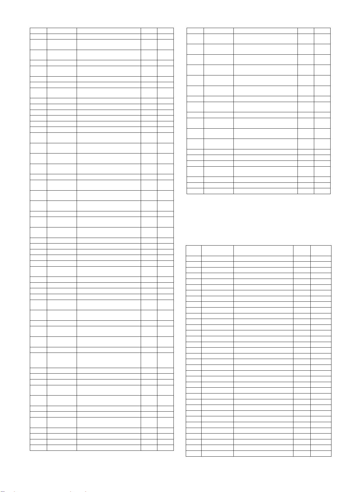
IC901:C0HBA0000246
8 DIN D signal input port. I 1.81
9 FEC LPF capacitor connection port for
FE signal. O1.76
10 RFMON LSI build-in analog signal monitor
port. O1.66
11 VREF VREF voltage output port. O 1.70
12 JITTC Capacitor connection port for JIT
signal. O0.01
13 EIN E signal input port. I 1.80
14 FIN F signal input port. I 1.80
15 TEC LPF capacitor connection port for
TE signal. O3.35
16 TE TE signal output port. O 1.71
17 TEIN TE signal input port for TES. I 1.69
18 LDD Laser power detection output port. O 2.44
19 LDS Laser power detection input port. I 0.17
20 AVSS GND for analog. - 0.03
21 AVDD VDD for analog. - 3.35
22 FDO Focus control signal output port.
D/A output. O1.61
23 TDO Tracking control signal output port.
D/A output. O1.66
24 SLDO Thread control signal output port.
D/A output. O1.92
25 SPDO Spindle control signal output port.
D/A output. O1.77
26 VVSS1 Gnd for build-in VCO. - 0.04
27 PDOUT1 Phase comparison output port1 for
build-in VCO control. O1.24
28 PDOUT0 Phase comparison output port0 for
build-in VCO control. O1.24
29 PCKIST PDOUT01 output port for current
setting. I1.15
30 VVDD1 VDD for VCO. - 3.36
31 DMUTEB DMUTEB (GENERAL) output
port. O3.35
32 PUIN PUIN (GENERAL) I/O port.Built-in
pull-up resistance. I/O 4.98
33 DEFFCT Detection signal output port. O 0.04
34 FSEQ Synchronous signal output port. - 3.34
35 C2F C2 error signal output port. O 0.04
36 DVDD VDD for Digital. - 3.36
37 DVSS GND for Digital. - 0.03
38 DVDD18 VDD capacitor connection port for
digital circuit. O1.61
39 MONI 0 Monitor port 0. O 3.36
40 MONI 1 Monitor port 1. O 0.04
41 DVDD VDD for Digital. - 3.36
42 DVSS GND for Digital. - 0.04
43 CE Host IF:Communication enable
signal input port. I1.32
44 CL Host IF:Data transfer clock input
port. I3.96
45 DI Host IF:Data input port. I 3.96
46 DO Host IF:Data output port.Pull-up is
necessary. O3.35
47 RESB "Reset input port.Make it ""L""
when power on." I5.15
48 INTB Interrupt signal output port.(Servo) O 0.05
49 SUB_READY 0 For host u-com IF:SUB-RDY out-
put.Pull-up resistance is neces-
sary.
O4.82
50 CD_MUTE 0 General I/O port2. I/O 4.98
51 LOW_BATI General I/O port1. I/O 0.04
52 CONT General I/O port0. I/O 0.04
53 OSCCNT OSCOFF control port.Connected
with 0V when reset. I3.34
54 STREQ Stream data demand signal output
port. I/O 0.08
55 STCK Clock input port for stream data. I/O 0.03
56 STDATA Stream data input port. I/O 0.04
57 TEST 1 Input port for test.Needed con-
nect with 0V. I0.03
58 DATA Lch/Rch data output port. O 0.05
59 DATACK Clock output port. O 3.35
60 LRSY Lch/Rch clock output port. O 0.05
61 VVDD 2 VDD for build-in VCO. - 3.35
Pin No. Port Description I/O (V) 62 VPREF 2 Built-in VCO oscillation cooking
stove setting input terminal. I0.05
63 VCOC 2 Built-in VCO control voltage set-
ting input port. I0.05
64 VPDOUT 2 Output port for built-in VCO con-
trol. O0.04
65 VVSS 2 GND for building VCO. Needed
connect with 0V. -0.03
66 DVDD18 VDD capacitor connection port for
digital circuit. O1.60
67 DVSS GND for digital system. Needed
connect with 0V. -0.04
68 DVDD VDD for digital system. - 3.35
69 DOUT Digital OUT output port. EIAJ for-
mat. O0.04
70 AMUTEB AMUTEB (general) ouput port. O 3.35
71 XVSS GND for oscillation circuit. Needed
connect with 0V. -0.03
72 XOPUT Connected of 16.9344MHz oscilla-
tion. O1.54
73 XIN Connected of 16.9345MHz oscilla-
tion. I1.59
74 XVDD VDD for oscillation circuit. I 3.32
75 LCHO L channel output port. O 3.33
76 LRVDD VDD for LR channel. - 1.66
77 LRVSS GND for LR channel. Needed con-
nect with 0V. -1.68
78 RCHO R channel output port. O 0.00
79 AVDD VDD for analog. - 0.00
80 SLCO Slice level control output port. O 1.68
Pin.
No. PORT Description I/O (V)
1 P1 General-purpose output. O 5.1
2 P2 General-purpose output. O 0
3P3 N.C. O 0
4S4 N.C. O 2.58
5 S5 Segment outputs. O 2.58
6 S6 Segment outputs. O 2.58
7 S7 Segment outputs. O 2.58
8 S8 Segment outputs. O 2.58
9 S9 Segment outputs. O 2.58
10 S10 Segment outputs. O 2.58
11 S11 Segment outputs. O 2.58
12 S12 Segment outputs. O 2.58
13 S13 Segment outputs. O 2.58
14 S14 Segment outputs. O 2.58
15 S15 Segment outputs. O 2.58
16 S16 Segment outputs. O 2.58
17 S17 Segment outputs. O 2.58
18 S18 Segment outputs. O 2.58
19 S19 Segment outputs. O 2.58
20 S20 Segment outputs. O 2.58
21 S21 Segment outputs. O 2.58
22 S22 Segment outputs. O 2.58
23 S23 Segment outputs. O 2.58
24 S24 Segment outputs. O 2.58
25 S25 Segment outputs. O 2.58
26 S26 Segment outputs. O 2.58
27 S27 Segment outputs. O 2.58
28 S28 Segment outputs. O 2.58
29 S29 Segment outputs. O 2.58
30 S30 Segment outputs. O 2.58
31 S31 Segment outputs. O 2.58
32 S32 Segment outputs. O 2.58
33 S33 Segment outputs. O 2.58
34 S34 Segment outputs. O 2.58
35 S35 Segment outputs. O 2.58
Pin No. Port Description I/O (V)
cq5109u.book Page 6 Thursday, June 30, 2011 3:27 PM