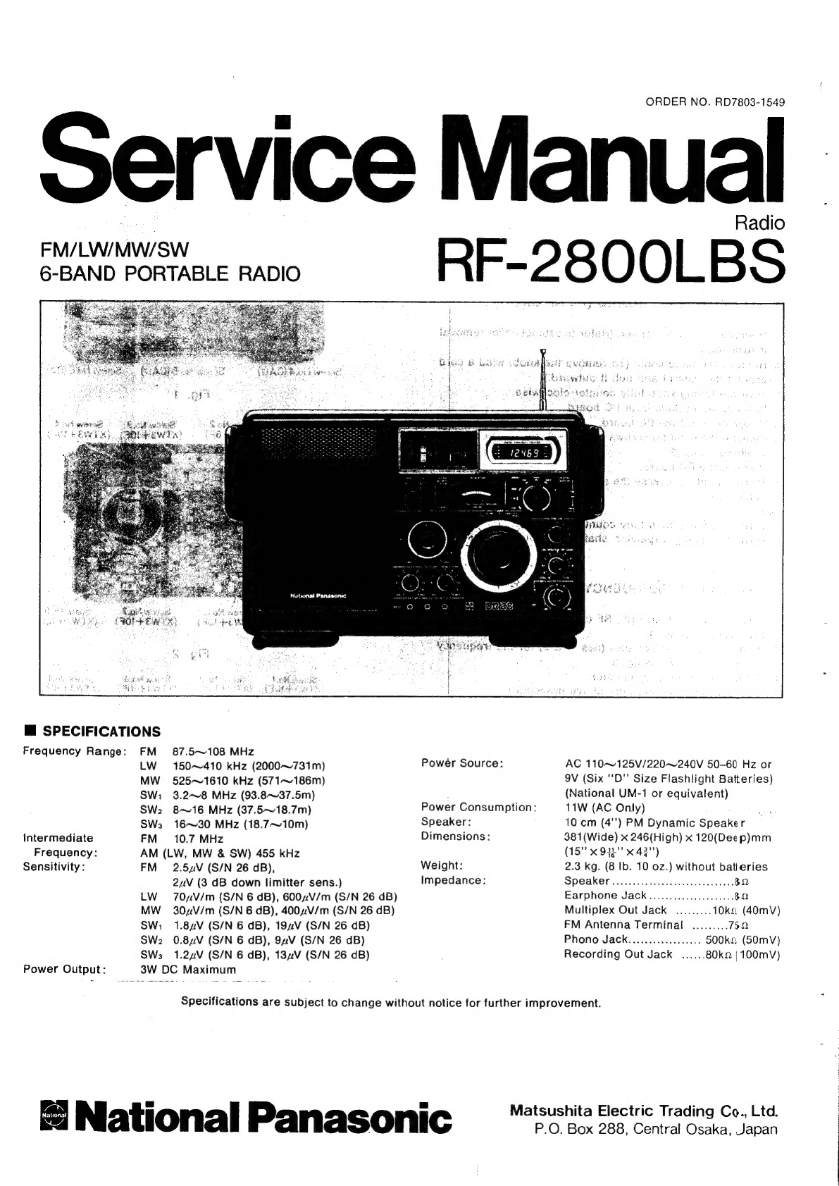
Panasonic RF-2800LBS Manual
Other Panasonic Radio manuals

Panasonic
Panasonic RF-D30BT User manual

Panasonic
Panasonic TBB 120335 User manual

Panasonic
Panasonic SE-5508 User manual

Panasonic
Panasonic RF-ND200R User manual

Panasonic
Panasonic RF-U350 User manual

Panasonic
Panasonic RF-B65 Instruction sheet

Panasonic
Panasonic R-1105 User manual

Panasonic
Panasonic RX-M40 User manual

Panasonic
Panasonic RF-SW70 User manual

Panasonic
Panasonic RF-521 User manual

Panasonic
Panasonic SG-5090 User manual

Panasonic
Panasonic TOYOTA CQ-MS7920A User manual

Panasonic
Panasonic RF-4800 User manual

Panasonic
Panasonic RF-D100BT User manual

Panasonic
Panasonic RF-D10EG User manual

Panasonic
Panasonic RC-D8 User manual

Panasonic
Panasonic RF-D10 User manual

Panasonic
Panasonic RF-D10EB User manual

Panasonic
Panasonic RF-D10 User manual

Panasonic
Panasonic RF-D1 User manual