Pine Technology PT-429G User manual

-.
=.-
._,
*‘.
:
486 MAIN BOARD
(25/33/40/50
MHz)
.
.i
USER’S MANUAL
.
It runs with
NetWare
e$
Recycled Paper

BEFORE INSTALLING THIS 486 MAIN BOARD PLEASE READ
THIS MANUAL COMPLETELY AND
RETAIN
IT FOR
FUTURE
REFERENCE.
The Green Connection
:
Please refer to page 5. section 1.14
Note
:
15-30
For the first
time
installation with error message on the screen, please leave the system on for about
minutes to recharge the battery, then you can enter the system configuration.
Leave your system on for about 24 hours to recharge the battery fully.
If you have switched off the computer system for more than
two
weeks, you might be required to repeat step
2 to recharge the battery fully.
Any hard disk cable longer than the standard type is not recommenced for used with
PT-429G.
Too long
hard disk cable will make the Green PC circuit unable to monitor the hard disk activity.
Trademark Acknowledgments:
IBM PC, PC/XT and PC/AT all are registered trademarks of International Business Machines Corporation
lntel
IS
registered
trademark of Intel Corporation.
AMD is registered trademark of Advanced Micro Devices Inc.
AMI
IS registered trademark of American Megatrends Inc.
UMC IS registered trademark of United Microelectronics Corporation.
VESA is registered trademark of Video Electronics Standards Association.*
2

TABLE OF CONTENTS
SECTION 1
INTRODUCTION
.
1.1
Overview
..
.
..
..
.
..
. . . . .
.4
1.2
Check
List
,,__.....,,,,._,....,..___.,..,....,_,.,.,.._,.,........................................................................................ 5
1.3
Green
PC
Power
Management
. . . .
..
..
. . . . . . . . . . . . . . . . . . . . . . . . . . . . . . . . . . . . . . . . . . . . . . . . . .
...
. . . . . . 6
1.4
PT_429G System Package . . . . ..___....._....................................................................................,.,........... 6
SECTION 2SPECIFICATIONS
2.1
GeneralFeatures..
. .
.
...
..
. . . . . . . . . . . . . . . . . . . . . . . . . . . . . . . . . .
....
.7
2.2
Jumpers
and
Connectors
...
..
. . .
..
..
..
..
. . . . . . . . . . . . . . . . . . . . .
...
. . . . . . . . . .
...
...
.7
2.3
Cache
RAM
Table
,._.....,....,......_..,.,,.,...__..................,..........................,....................,.....................
12
2.4
Oscillator
Table
..
.....
...
... . . .
..
. . . . . . .
..
..... . . . . .
.....
. . . . . . . . . . . . . . . . . . . . . . . . . . . . . . . . . . . .
...
...
. . .
...
12
SECTION 3
I/O
CHANNEL SLOTS
3.1
I/O
Address
Map.. .
.
.
.
.
.
.
.
.
.
.
.
.
13
3.2
62-pin,
36-pin
I/O
Bus
,__......,.,_...,...............,..........................,.......................................................
14
3.3
1
12-Pin
VESA
I/O
BUS
..,..,..._............,........................._.....................,............................................
15
SECTION 4HARDWARE COMPATIBILITY
4.1
System
Timers...............................................................................................................................
.16
4.2
System
Interrupts
...........................................................................................................................
.I6
4.3
Direct Memory Access..
.................................................................................................................
.17
4.4
Real
Time
Clock and Non-Volatile
RAM
.......................................................................................
18
SECTION 5 AMI
BIOS SETUP
5.1
5.2
5.3
5.4
5.5
5.6
5.7
5.8
5.9
About CMOS Setup.
.......................................................................................................................
19
Entering
CMOS
Setupp
.................................................................................................................
...2
0
Getting
Help.
........................................................................................................................ ..........2
0
Using
Setup..
.................................................................................................................................
.20
Standard
CMOSSetup
..................................................................................................................
.21
Advanced CMOS
Setup
..................................................................................................................
22
Advanced
Chipsett
Setup
................................................................................................................
.24
Power
Managementt
Setup
.............................................................................................................
.25
Changing
the
Password
.................................................................................................................
.26
5.10
Hard Disk Utility
...........................................................................................................................
.27
5.11
Exiting Setup..
................................................................................................................................
27
SECTION 6
:
DIAGRAM
LAYOUT .....
.
.
.
.
.
.
.
.
.
.
.
.
.
.
.
.
.
.
.
.
.
.
.
.
.
.
.
.
.
.
.
..........
.
.
.
.
.
.
.
.
.
.
.
.
.
.
.
.
.
,..........................
28
3

SECTION
1
INTRODUCTION
1.1 Overview
PT-429G
offers
a 32-bit programming architecture compatible with the software base of the 486
microprocessor. It is a reliable main board using a UMC
chipset
and a multi-layer printed circuit hoard
The
chipset
consists of
UM82C491F-AC
and
UM82C493F
which provide the most cost effective and high
xperformance solution for a 486 computer system.
The
UK482C491F-AC
contains a sophisticated direct-mapped cache controller with write-back operation,
and
fast
page mode DRAM Controller, AT Bus control logic, data bus conversion logic, CPU reset logic,
clock generation for CPU, keyboard and timer,
DMA/refresh
logic and peripheral interface logic. The
UMC493F
contains a sophisticated VESA Controller which can run up to
5OMHz.
A block of
128K
memory of the system DRAM is used for system and video shadow RAM to increase the
system performance. The video shadow RAM consists of four 16K pages which can be enabled
respectively.
The
PT-429G
is a VESA Local Bus motherboard The three Local Bus slots fully comply with the VESA
(
Video Electronics Standards Association
)
Master mode specifications. This means
I/O
data can run as
fast as CPU. The speed of
I/O
peripherals can be dramatically increased by connecting VESA compatible
controller cards to the VESA Local Bus slots on the
PT-429G.
The
PT-429G
is a green design mother-board which means when there is no operation on the system for a
while (the period is software programmable), the
PT-429G
will slow down its original working frequency
to 8 MHz speed This will help to save the power consumption in order to protect our environment. The
PT-429G
is equipped
with
a
AUX
Green connector which can be connected up to four external Green
devices through our Green cable.
“This is an
ENERGY
STAR
compliant product.”
“The Environmental Protection Agency ENERGY
STAR
program defines that as an Ally of this
program the specified manufacturer must produce systems, or system components which enable a
computer system to operate and draw 30 watts or less of power in idle
mode.
Although the EPA do not
endorse any particular product or service, the program is designed to offer a cooperative effort between the
EPA and the component manufacturer (Ally) to provide energy saving products and education to
customers.”
“It runs with Netware”
PT-429G
was authorized by Novell to use the Novell Yes, It runs with Netware
certification
mark.

SECTION
1
INTRODUCTION
1.2
Checklist
FCC approval:
The
PT-429G
motherboard has been approved for FCC Class B when properly installed in a barebones
configuration using the following case/power supply:
Brand Model FCC
ID
ProcaseX-109
S/M
JPJPINE429G
109
Procase
PC-609 T/M JPJPlNE429G609
Procase PC-709 T/M
JPJPINE429G709
FCC Notice:
Information to the user
This equipment has been tested and found to comply with the limits for a Class B digital
device, pursuant
to Part 15 of FCC Rules. These limits are designed to provide reasonable protection against harmful
interference in a residential installation. This equipment generates, uses and can radiate radio frequency
energy
and,if
not installed and used in accordance
with
the instructions, may cause harmful interference to
radio communications.
However, there
is no guarantee that interference to radio or television
reception, which
can be determined by turning the equipment off and
on,the
user is encouraged to try to
correct the interference by one or more of the following measures:
l
Reorient or relocate the receiving antenna.
l
Increase the separation between the equipment and receiver.
l
Connect
the equipment into an outlet on a circuit different from that to which the
receiver is connected.
l
Consult the dealer or an experienced
radio/TV
technician for help and for additional
suggestions.
The user may find the following booklet prepared by the Federal Communications Commission helpful:
“How to
identify
and Resolve
Radio-TV
Interference Problems
”
This booklet is available from the U.S.
Government
Printing
Office, Washington, DC 20402, Stock No. 004-000-00345-4.
FCC Warning
The user is cautioned that changes or modifications not expressly approved by the manufacturer could
void the user’s authority to operate this equipment.
Note:In
or&r for an installation of this product to maintain compliance with the limits for a Class B
device, shielded cables and power cord must be used
Please check your
PT-429G
package to ensure that it contains the following items
:
-
PT-429G
Main Board
-
PT-429G
User’s Manual
If
any of these items are missing or damaged, please contact your local dealer or sales representative for
assistance.

SECTION 1
INTRODUCTION
1.3 Green PC Power Management
The Green PC mode is a state that minimizes the power consumption. Through the BIOS setting of the
PT-429G
can slow down the CPU clock to
8
MHz in Green PC mode. The
PT-429G
extends the Green PC
feature to four external devices (Green AUX
#l
to # 4) by the AUX Green connector
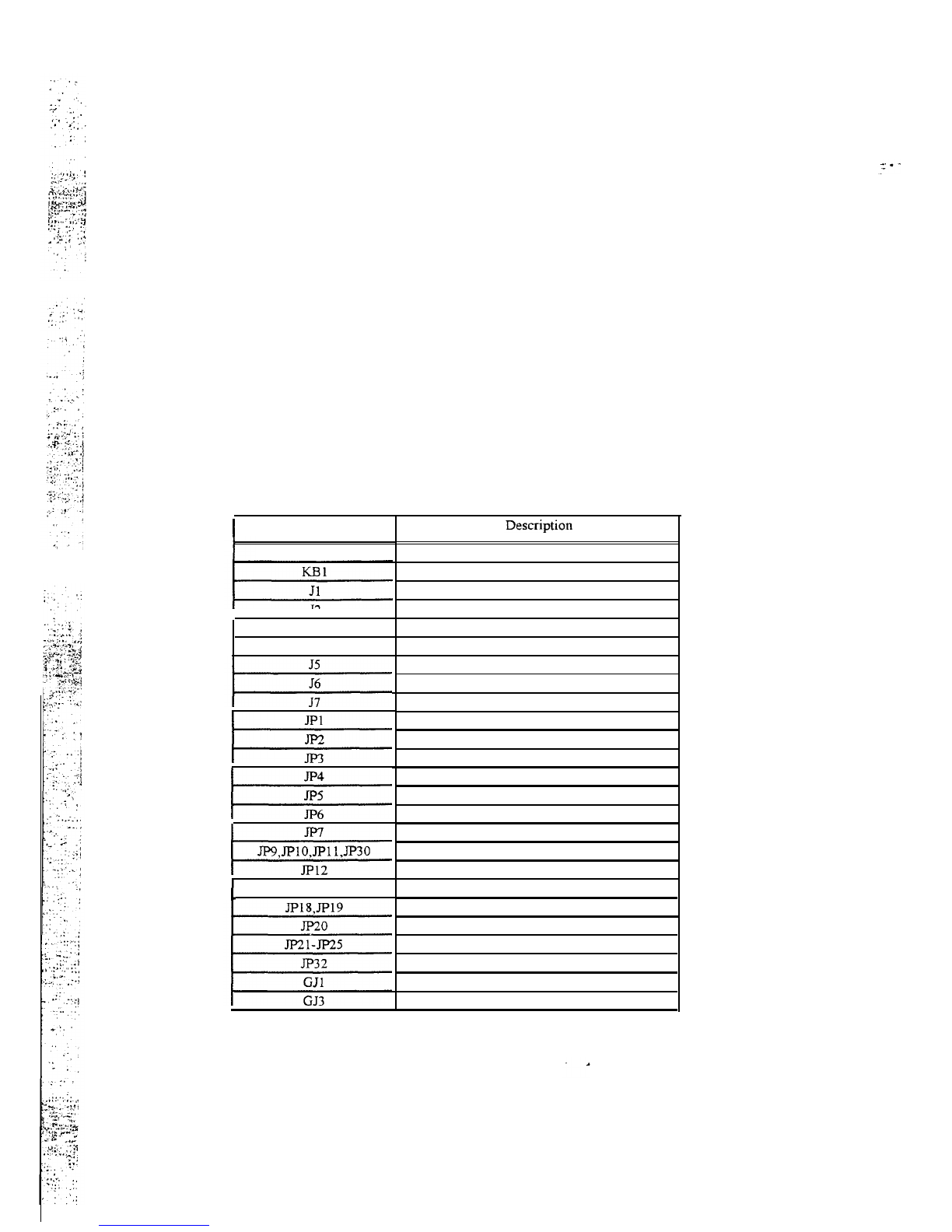
(J7
&
JP32). The
Green PC mode option of these Green AUX connectors are
:
-
Remove the sync signals from the video monitor,
-
Turn off video monitor power,
-
Turn off printer power,
-
Turn off hard disk drive power.
PT-429G
will be placed into Green PC mode as a result of one of the following events
:
-
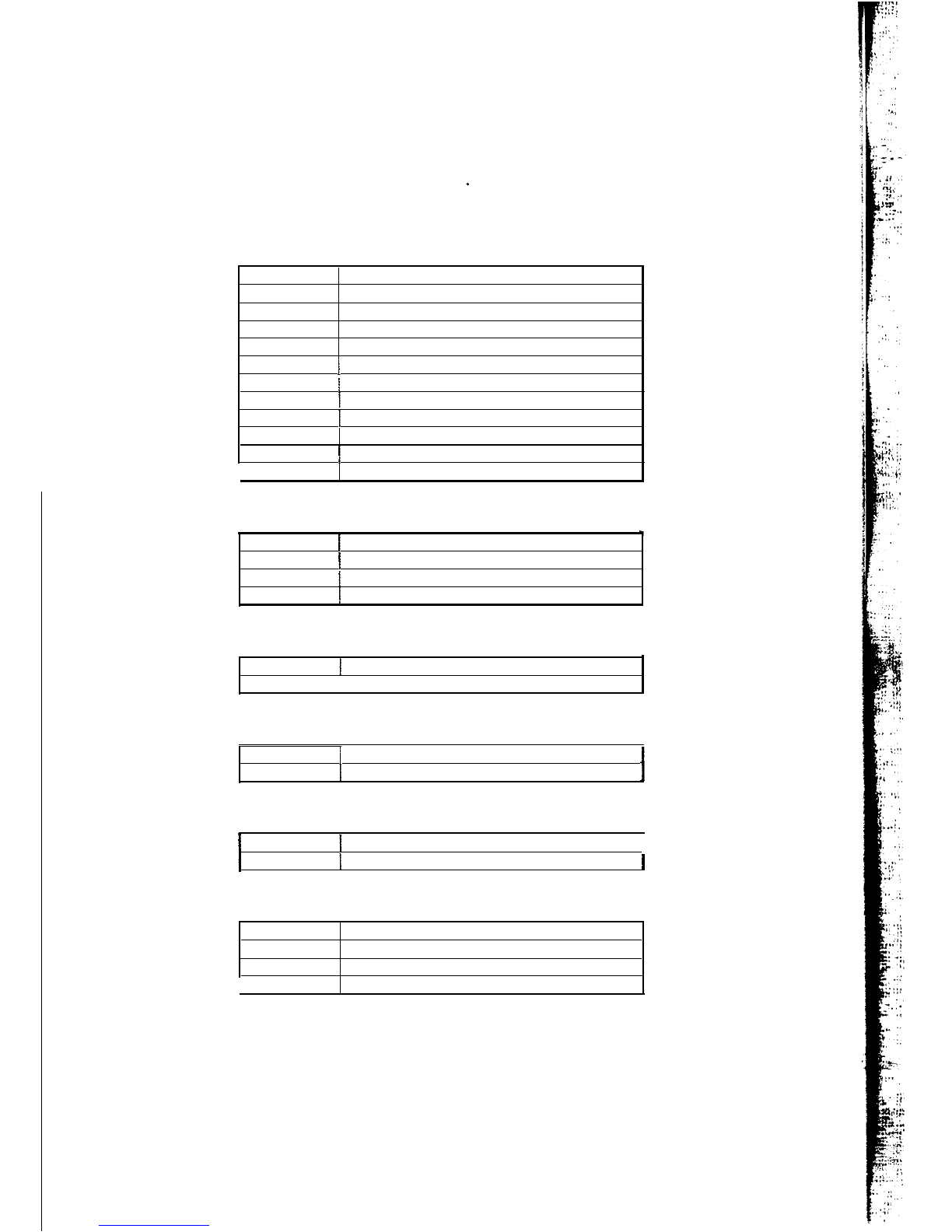
Power save button (GJl) is shorted.
-
Expiration of one of five independent Green PC Timers, the 1st timer is used to slow down CPU
speed. The Green PC Timers are software programmable which can configured in the “Power
Management Setup!’ option of the BIOS CMOS setup. (Refer to 5.8 Power Management Setup)
-
Execution of the system hot key for power down sequencing
<CTRL>
<ALT>
<\>.
Through the system activity monitoring and management, the PT-429G will not go into Green PC mode
(or leaves Green PC mode and back to normal mode) if any activity is detected on the following signals:
-
IRQ1
(Keyboard)
-
IRQ3 (COM2)
-
IRQ4 (COMl)
-
IRQ6
(FDD)
-
IRQ7 (LPTl)
-
IRQ14
(HDD)
1.4
PT429G
System Packages
The
PT-429G
mother-board can act as the nucleus to various system con&nations, in order to optimize
your total power saving The following is a brief introduction to add-on cards and peripherals suited to
the
PT429G
;-
(1)
Optimum
Power Saving system package.
PT-429G
mother-board
Monitoring
COMl,
COM2, LPT
1,
Keyboard, Floppy Drives, Hard Drives.
PT523G,
PT524G.
PT528G
Cirrus Logic VGA Cards
Turning off the vertical
&
horizontal sync of monitors through the unique PT-429G hardware connection.
This hardware connection works in any environment @OS, WINDOWS etc), whereas software drivers
only work in WINDOWS.
PI-626 UMC VESA Local Bus IDE I/O Card
Powerful controller card with added Green
driver.
ECO
PAD
This
external device connects to the second unique PT-429G connector to add on/off switching to
peripherals such as printers, monitors and scanners
-
All timing and on/off controlled by the
PT429G
mother-board. Utilizing a Zero Voltage Protection Circuit the
ECO
PAD ensures safe and reliable on/off
switching which will not harm your peripherals.
Testing results have shown that a system using the above products consumes only 17.6 watts of power at peak
voltage of 220v.
The effective watts RMS) is less than 10 watts. Add an
ECO
PAD to this configuration
and this covers your system, monitor, printer and scanner.
Alternative system packages.
The
PT429G
mother-board is equipped with two unique green connectors, however it can also use
conventional VGA cards to add power saving features to monitors using their respective software driver(s).
All
efforts are made to ensure the PT429G is compatible with a wide range of add-on cards.
For
further details on
PT523G,
PT524G,
PT528G,
PT626 and the
ECO
PAD please contact your local dealer or
sales representative for assistance.

SECTION 2
SPECIFICATIONS
.
2.1
PT-429G
System Board Specifications
*
*
*
*
*
*
*
*
*
*
*
*
*
100% IBM AT compatible.
Applied High performance CMOS technology.
Supports up to
48MB
memory on board.
Mix
256K,
lM, and 4M SIMM (8 bit/32 bit) Module DRAM memory
32K,
64K,
128K,
256K
cache memory size selectable.
Fast CPU reset and Fastgate A20 logic.
Speed switching with hardware and software selection.
Board size 220 mm by 250 mm.
Six 16-bit ISA slots; one S-bit ISA slot.
Three VESA slots (Master Mode).
Clock chip design makes CPU speed changing easier.
I/O
slot signal protector on:
IRQ9,
DRQ2,
OWS#.
Green feature to slow down CPU speed
&
control 4 external Green devices.
2.2 Jumpers and Connectors
I
Jumpers
/
Connector
Pl
J3
J4
I
I
/xi+-
L
JPl3-JPI 7
Power Supply Connector
Keyboard Connector
External Battery Connector
Reset Switch
Turbo Switch
Turbo LED Connector
Speaker Connector
Power LED
&
Kevlock Connector
Green
AUX
#
1 Connector
On-board Battery Enable Connector
Power Good Select
VGA Card Select
Master Mode Select
CPURDY#
Delav I-T Select
PADS# Delay 1-T Select
Test Logic Enable Select
Clock Chip Speed Select
VESA Speed Select
Cache Size Select
CPU Type Select
VESA Wait State Select
Bank of SIMM Select
Green
AUX
#
2 Connector
Green Enable Switch
MEGA/MULTI
KEY Select
7

SECTION
2
SPECIFICATIONS
2.2 Jumpers and Connectors
Pl Power Supply Connector Pin Assignment
1
Power Good
2
+5V
3
+12V
4
-12V
5
Ground
6
1
Ground
7
j
Ground
8
/
Ground
9
j
-5v
10
+5V
11
1
+5V
Jl
External Battery Connector Pin Assignment
1
[
External battery Vcc
(+6V
DC)
2
1
NC
3
j
Ground
4
1
Ground
J2
:
Reset Switch Connector
Open
Short
1
Normal
1
Reset
J3
Turbo Switch Connector
Open
1
Turbo speed
Short
1
Lower speed (Soft-key turbo switch disable)
I
J4
Turbo LED Connector
I
1
/
LED Cathode
1
I
2
1
LED Anode
I
J5
Speaker Connector Pin Assignment
1
Speaker data
2
NC
3
Ground
8

SECTION
2
SPECIFICATlONS
2.2 Jumpers and Connectors
J6
:
Keyboard Lock
&
Power LED Connector Pin Assignment
si
JP1
:
On-board Battery Enable Select
Open
/
On-board battery disconnect
t..
”
,....
Short
t3ldoard~~
cmect
JF2
: Power Good Select
JP3
:
VGA Card Type Select
I
f-2
1
Normal
VGh
m-d
2-3
1
POWER-9000 VGA card
JP4
:
Master Mode Select
l-2
[
Enable
Cx487S
&
MC43 only for Master Mode
i
2-3
1
Normal
3
VESA
h&&x
JP5:
CPURDY#
Delay
I-T
State Select
\
1-2
1
No
deiay
for
sow.
WSA,
2-3
1
Delay 1-T state for
5OMHz
VESA
JP6:
PADS#
Delay I-T State Select
d&y
for
SOMHZ
VE!iA
ay 1-T state for
5OMHz
VESA
JP7.
Test Logic Enable
(486DX2)
Select
!
OPEN
1
Enabfe
CW
Test Logic
CLOSE
1
Disable CPU Test Logic
9

SECTION
2
SPECIFICATIONS
2.2 Jumpers and Connectors
JP9,JPO.JPI
l,JP30: Clock Chip Speed Select
Clock Chip =
AvaSem
AV9 107-05 (U34)
JPlO
I
JPll
25MHz ON OFF
33MHz
4oMHz
,
JP30
2-3
2-3
2-3
I
5oMHz
I
ON
I
OFF l-2
I
Clock Chip =
Chrontel
CH9007E (U35)
I
I
JP!J
JPIO
.JPll
I
25MHz ON ON ON
33MIIz-
..
i,
.:
:,:
j;.,
.@j+q
i
:..::
I:..:
‘~‘:~‘:i:Q~~“.::.I’:-..‘p:.,.:~:’.I~.:~i
$-r@
,,..,..
4oMHz ON OFF ON
SOMHZ
OFF OFF OFF
Clock Chip = MX83 15 (U28)
JP9
JPlO
JPll
25MHz OFF OFF ON
33MJrl.z
ON ON ON
4OMHZ
OFF ON ON
SOMHi!
ON OFF OFF
JPl2:
VESA Speed Select
IOpen
[CFwspeed~=33MHz
Short
1
CPU speed
>
33MHz
.JPi
3-JPI
7.
Cache Size Select
32KEl
[
64KB 128KB
1
256KB
JP13
Open Open 2-3
I
1-2
JPl4
2-3
1-2
2-3
l-2
JPI
8,JPl9:
CPU Type Select
486SX
486DXDX2
P24N/P24T
JP18 2-3
t-I&3-a
l-2,3-4
JPl9
Open
1-2
2-3
JP20:
VESAWait
State Select
t
Open
1
0
Wait
State
Short
j
1
wait
State
10

SECTION 2
SPECIFICATIONS _
SIMM
memory must begin from ‘Bank 0’
The following three Banks are available
.
.
.
30-pin
Bank x 1
(4pcs
of
30-pin
sockets =1 Bank
-
4pcs
of
30-pin
SIMM
required. Bank must be completely
filled).
.
72-Pin
Bank x 1 (lpc of 72-pin socket = 1 Bank
-
only
Ipc
of
72pin
SIMM
required).
l
72-Pin
Bank x
1
(lpc of
72-pin
socket = 1 Bank
-
only lpc of
72-pin
SIMM required).
Any of these Banks can be selected as ‘Bank 0’. Therefore you can begin with
3Qin
SIMM modules and upgrade
using 72-pin
SLMM
modules, or visa-versa. Please see tables below for necessary jumper settings.
2.2 Jumpers and Connectors
JP21-JP25
:
Bank of SIMM Select
8bitSIMMcanbeselectedatBANKOorBANK2
Bank0
I
Bank2
JP21
1-2
2-3
32 bit SIMM can be set as follow (some 32 bit SIMM can occupy 2 BANK per SIMM)
Single BANK 32 bit SIMM:
SlMMScanbeBANKOorBANKl
,Bank0
JP22
1-2
JP23
OF!?
SJMM6canbeBANKlorBANK2
Bank1
JP24
1-2
JP25
OFF
Bank1
2-3
OFF
Bank2
2-3
OFF
Double BANK 32 bit SIMM:
SIMh45canbeBANKO&lorBANK1&2
I
Bar&O&l
1
Bat&l&2
JR?2
l-2
2-3
L
JP23
I
l-2
I
2-3
I
SlMM6canbeBANK1&2orBANK2&3
Bankl&2
Bank2&3
JP24
l-2
2-3
JR25
l-2
2-3
J7:
Green AUX # 1 Connector
1
Green
AUX
Output #
1
2
Green
AUX
Output #
2
3
Green
AUX
Output #
3
4
Green AUX Output #
4
-.-
7
Ground
8
Ground
9
Ground
11

SECTION 2
SPECIFICATIONS _
2.2 Jumpers and Connectors
JP32: Green AUX
#
2 Connector
I
1
/
Green AUX
Outnut
if
1
I
I
2
/
Green AUX Output
#
2
I
GJ
1:
Green Enable Connector (For Green case panel switch only)
t
Open
[
Normal
Operation
Short
1
Enable Green Function
I
GJ3:
MEGA
/
MULTI KEY Select
12
1
AMI
MEGAKEY
KeybardBIOS
2,3
1
Phoenix
MULTIKEY
Keyboard BIOS
1
1
Default Setting
2.3 Cache Memory Table
FT-429G 80486 VESA system board supports 32KB/64KB/128KB/256K cache size.
Size
SRAMType Quantity
Designation TAG RAM (U25)
32KB
8Kx8
4 pcs.
Bank0
8K
x 8
64KB
SK x 8
8 pcs.
BankO&Bankl 8Kx8
128KB
32Kx8
4 pcs.
Bank0
8Kx8
256KB
32Kx
88
pcs.
BankO&Bankl
32Kx
8
Note : Bank 0
(lJZl,U22,U23,U24),
Bank 1
(lJl4,lJl5,lJl6,Ul7)
Refer to Section 2.2
JPlLJPl7
jumper settings with different Cache sizes.
2.4 Oscillator Table
CPU Speed
804868X-25
80486DX-33
Am486TMDX-40
80486DX-50
80486DX2-50
80486DX2-66
Oscillator
25MI-k
33MHz
4oMHz
SOMHZ
25MI-k
33MHz
12

SECTION 3
_.
.
-
INPUT
/
BUTPUT
CHANNEL SLOTS.
The input/output channel of PT-429G supports :
*
Refresh of system memory from channel microprocessors
*
Selection of data accesses:
S-bitil6-bit
*
Interrupts
*
DMA channels
*
I/O wait-state generation
* Open-bus structure
*
Up to
5OMHz
I/O speed under
VJZSA
standard
3.1
I/O
Address Map
Hex Range Devices
Usage
000-O
1F
DhJA Controller 1 System
020-03F
Interrupt Controller 1 System
040-05F
Timer
System
060-06F
8042 ( Keyboard
>
System
070-07F
Real Time Clock,
NMI
Mask
System
080-09F
DMA Page Register System
OAO-OBF
Interrupt Controller 2
System
OCO-ODF
DMA Controller 2 System
OF0
Clear Math Co-processor Busy System
OF1
Reset Math Co-processor System
OFbOFF
Math Co-processor System
lFO-IF8 Fixed Disk I/O
200-207
Game I/O I/O
27%27F
Parallel Printer Port 2
I/O
2F8-2FF Serial Port 2 I/O
300-3
1F
Prototype Card I/O
360-36F
Reserved
YO
378-37F
Parallel Printer Port 1
I/O
380-38F
SDLC, Bisynchronous 2 I/O
3AO-3AF
Bisynchronous 1 I/O
3BO-3BF
Monochrome Display and Printer Adapter
I/O
3CO-3CF
Reserved I/O
3DO-3DF
Color/Graphic Monitor Adapter I/O
3FO-3F7
Floppy Diskette Controller I/O
3F8-3FF Serial Port 1
VO
*-*_
.
.
.h;
13

SECTION 3
INPUT /OUTPUT CHANNEL SLOTS
*
3.2 62-Pin. 32-h ISA I/O Bus.
GND
RESET DRV
+5V ED
mQ9
-5V DC
DRQ2
-12VDc
ows
+12VDc
GND
-SMTEMW
-SMEMR
-row
-1OR
-DACK3
DRQ3
-DACK 1
DRQ
1
-REFRESH
CLK
mQ7
BQ6
RQ5
mQ4
mQ3
-DACKZ
-l-/C
BALE
+sVDc
osc
GND
-MJZM
CS16
-UO
CS16
IRQ
10
IRQ
II
lRQ
12
WQ
15
IRQ 14
-DACK 0
DRQ 0
-DACK 5
DRQ 5
-DACK 6
DRQ 6
-DACK 7
DRQ 7
+5V
DC
-MASTER
GND
REAR PANEL
Bl I
I
Al
B2
I
B3 I
:zi
B4 I I A4
B5
I
j
A5
B6 II
‘46
B7 II A7
B8
I
I
A8
B9 II A9
BlO
)
j
A10
BIl
/
/
All
812
B13
B14
B15
B16
B17
Bl8
B19
B20
B21
B22
B23
B24
B25
B26
B27
B28
B29
B30
B31
Dl
D2
D3
D4
D5
D6
D7
D8
D9
DlO
Dll
D12
D13
D14
D15
D16
D17
D18
A12
Al3
Al4
Al5
Al6
Al7
Al8
Al9
A20
A21
A22
A23
A24
A25
A26
A27
I
I
/
A28
I A29
I A30
I
A31
i_
I
Cl
I
c2
I C3
I C4
I
C5
I
C6
I
C7
I C8
I
C9
/
Cl0
I
Cl1
;
Cl2
I
Cl3
I
Cl4
I
Cl5
1
Cl6
1
Cl7
/
Cl8
-I/O
CH CK
SD7
SD6
SD5
SD4
SD3
SD2
SD1
SD0
-I/O
CH RDY
AEN
SA19
SA18
SA17
SA16
SA15
SA14
SA13
SA12
SAll
SAlO
SA9
SA8
SA7
SA6
SA5
SA4
SA3
SA2
SAl
SAO
LSBHE
LA23
LA22
LA21
LA20
LA19
LA18
LA17
-MEMR
-MEMW
SD08
SD09
SD10
SD11
SD12
SD13
SD14
SD15
13

SECTION 3
INPUT
/
OUTPUT CHANNEL SLOTS
3.3 I12-Pin VESA I/O Bus for
FT-429G.
REAR PANEL
DATA00
DATA02
DATA04
DATA06
DATA08
GND
DATIO
DATl2
VCC
DA-I’14
DAT16
DATl8
DAT20
GND
DAT22
DAT24
DAT26
DAT28
DAT30
VCZ
ADR3 I
GND
ADR29
ADR27
ADR25
ADR23
ADRZI
ADR19
GND
ADR17
ADRIS
VCC
ADR13
ADRll
ADR09
ADR07
ADROS
GND
ADR03
ADROZ
N/C
RESET#
D/CU
MAo#
WIR#
RDYRTN#
GND
mQ9
BRDY#
BIAST#
m0
mi
GND
LCLK
VCC
LBS16#
B1
I
~32
I
B3
I
B4
I
B5
I
B6 I
B7 I
BS
I
139
I
BlO
I
Bll
/
B12
/
B13
[
B14
1
B15
1
B16
1
B17
1
818
I
B19
j
BZO
I
B21
I
B22
/
B23
)
B24
I
B25
)
B26
I
B27
j
B28
/
B29
)
B30
I
B31
)
B32
(
833
B34
B35
B36
B37
B38
B39
B40
B41
B42
BJ3
B44
B45
B48
849
B50
851
B52
B53
B54
BSS
B56
B57
B58
15
I
Al
IE
I A4
IZ
I
A7
I
A.8
/
20
1
All
I
Al2
1
A13
1
Al4
1
A15
/
A16
I
A17
I
A18
I
Al9
I
,420
I
‘421
I
A22
I A23
I
A24
I A25
I
~26
I
A27
I
~28
I A29
I
MO
I
A31
I A32
A33
A34
A35
A36
A37
A38
A39
A40
A41
A42
A43
A44
A45
A48
A49
A50
A51
A52
A53
A54
A55
A56
A57
A58
DATOl
DAT03
GND
DATOS
DAT07
DAT09
DATll
DAT13
DATl5
GND
DAT17
VCC
DAT19
DA?2
1
DAT23
DAT25
GND
DAT27
DAT29
DAT3 1
ADR30
ADR28
ADR26
GND
ADR24
ADR22
VCC
ADR20
ADRlS
ADR16
ADR14
ADR12
ADRIO
ADROS
GND
ADR06
ADR04
WBACK#
BEO#
VCC
BEl#
BE2#
GND
BW#
AD.%
LRDY#
LDEV<XM
LEcDO<XM
GND
LGNT<X>#
VCS
m2
m3
m4
LKEN#
LFIADS#

SECTION 4
HARDWARE COMPATIBILITY
4.1
System Timers
The system has three programmable timer/counters controlled by an Intel 8254-2 timer/counter chip.
These are channel 0 through 2, defined as follows
:
Channel 0
GATE 0
CLKINO
CLK OUT 0
Channel
1
GATE 1
CLK IN
1
CLK
OUT
1
Channel 2
GATE 2
CLK IN 2
CLK OUT 2
Note : Channel is programmed to generate a 15 microsecond period signal.
4.2
System Interrupts
I
System timer
Tied on
1.190Mhz
OSC
8259A IRQ 0
Refresh Request Generator
Tied on
1.190Mhz
OSC
Request Refresh Cycle
I
Tone Generation for speaker
Controlled by bit 0 of hex 61 PPI bit
1.190Mhz
OSC
Used to drive the speaker
Sixteen levels of system interrupts are provided by the 80286 NMI
&
two 8259A interrupt controller
chips. The following shows the various interrupt-level assignments in decreasing priority
:
Level Function
NM1
Parity or I/O channel check
CTLR 1
2
CTLR
IRQO Timer output 0
IRQ 1
Keyboard (Output buffer full)
mQ.2
Interrupt from
CI’LR
2
RQ
8
Real time clock interrupt
IRQ 9
Software redirected to INT
OAH(IRQ
2)
IRQ 10 Reserved
IRQ 11
Reserved
IRQ 12 Reserved
IRQ 13
Numeric co-processor
IRQ 14 Fixed disk controller
IRQ 15 Reserved
IRQ3
Serial Port 2
IRQ4
Serial Port 1
RQ5
Parallel Port 2
RQ6
Diskette controller
IRQ
7
Parallel port 1
16

SECTION 4
HARDWARE COMPATIBILITY
*
4
3 Direct Memory Access
Each DMA channel is supported by the system. Two Intel 8237-5 DMA controller chips (Four channels in
each
chtp)
are used. DMA channels are assigned as follows
:
Channels from 0 through 3 are contained in DMA controller 1. Transfers of 8-bit data S-bit
I/O
adapters
and 8-bit or 16-bit system memory are supported by these channels. Each of these channels will transfer
data in 64KB blocks throughout the 6-megabyte system address space.
Channels from 4 through 7 are contained in DMA controller 2. To cascade channels 0 through 3 to the
microprocessor, use channel
1.
Transfer of
16-bit
data between 16-bit adapters and 16-bit system memory
are then supported by channels 5, 6,
&
7. DMA channels from 5 through 7 transfer data in
128K
blocks
throughout the 16-megabyte system address space.
These channels will not transfer data on odd-byte bowdaries.
The address for the page register is as follows :
Page Register
L/O
HEX address
DMA
channel
0
0087
DMA
channel
1
0083
DMA
channel
2
0081
DMA
channel
3
0082
DMA channel 5
008B
DMA
channel
6
0089
DMA channel 7 008A
Refresh
008F
Address generation for the DMA channels is as follows
:
For DMA channels 3 through 0
:
Source
Address
(
DMA
Rage
Registers
8237A-5
A23
.._.
Al6 Al5 Al
For DMA channels 7 through 5
:
Source
1
Address
1
DMA
Rage
Registers
8237A-5
A23
.._._
Al7
Al6
A0
I
Note
:
The BHE and
A0
addressing signals are forced to a logic 0. DMA channel
addressees do not increase or decrease through page boundaries (64KB for
channels 0 through 3 and 128 KB for channels 5 through 7).
17
_.
.
-

SECTION 4
HARDWARE COMF’ATIBILITY
4.4 Real Time Clock and Non-Volatile RAM
The real time clock and its 64 bytes of RAM information are backed up by
3.6V
rechargeable DC battery
(or 6V external battery). The internal clock circuitry uses 14 bytes while the rest is allocated to system
configuration.
Real time clock address
:
18

SECTION
5
_.
.
-
AM1
BIOS Setup
*
5
1
About CMOS Setup
After the
PT-429G
mainboard has been integrated into the system, you need to run the Setup Program to
set system configuration. Upon finishing the Setup Program is then stored in read-only memory (ROM),
and can only be accessed when you turn on or reset the system.
The settings you specify with the Setup program are recorded in a special area of memory called CMOS
RAM. This memory is backed up by a battery so that it will not be erased when you turn off or reset the
system. Whenever you turn on the power, the system reads the settings stored in CMOS RAM and
compares them to the equipment check conducted during the POST. If an error occurs, an error message
will be displayed on screen, and you will be prompted to run the Setup program.
The
AMI
BIOS Setup program is accessed through a menu which allows you to easily configure your
system. Standard CMOS Setup allows you to record basic system information regarding date and time,
video type and installed drives. Advanced CMOS Setup gives you access to the advanced features
supported by the
AM1
BIOS and your mainboard
chipset.
5.2 Entering CMOS Setup
-
When you turn on the system and in the course of the system
POST,
you will be presented with the
screen depicted below.
To enter the Setup program at this time, press the [Del] key. This will display the first page of the
AMI
BIOS Setup menu.
-
If you do not press the
PEL]
key at the right time, press [Ctrl-Ah-Del] to restart the system and try
again.
-
If you do not press the key at the correct time and the system fails to boot, an error message
KEYBOARD ERROR will be displayed and you will again be asked to
:
RUN SETUP UTILITY
Press
<F
l>
to resume
If you press and hold the [Ins] key while the system is booting until you bear a single beep, the
default Setup values will be loaded into CMOS. Release the key after the beep to prevent a
keyboard error.
After you enter into the Setup Program, a main menu of the
AMI
Setup Program is shown,
-
Select Standard CMOS Setup to access the Standard CMOS Setup menu, which is discussed in section
5.5.
19

SECTION
5
AMI BIOS SETUP
.
5.2 Entering CMOS Setup
Select Advanced CMOS Setup to access the Advanced CMOS Setup menu, which is discussed in
section 5 6.
The Advanced
Chipset
Setup to access the Advanced
Chipset
Setup menu, which is discussed in section
5.7.
Select Auto Configuration with BIOS Defaults to load the default system values. You will be prompted
for confirmation, and notified that the values have been loaded.
Select Auto Configuration with Power-On Defaults to load the default power-on values, which disable
all
performance options. This option serves a useful diagnostic function in the event of a compatibility
problem. You will be prompted for confirmation, and notified that the values have been loaded.
Select Change Password to access the password security menu, which is discussed in section 5.8 below.
Select Hard Disk Utility to access the hard disk utility menu, which is discussed in section 5 9 below.
Select Write to CMOS and Exit to save your configuration and exit the Setup program. You will be
prompted for confirmation before the changes are written to CMOS and the system reboots.
Select Do Not Write to CMOS and Exit to cancel any changes to your configuration and exit the Setup
program. You will be prompted for confirmation before the system reboots.
A warning message will appear each time you select Standard or Advanced CMOS Setup.
5.3 Getting Help
-
Help screens are displayed for each option in the Standard CMOS Setup menu. and can be accessed in
the Advanced CMOS Setup menu by pressing
Fl],
A “popup” window till appear, similar to the one
ptctured below, listing the available selections for that option. To exit the Help window, press any key.
-
If you have trouble reading the Setup menu, toggle the menu colors by pressing
[F2]
for background
color and
F3]
for foreground color.
5.4 Using Setup
The following keys and key combinations are used to maneuver among Setup options and to change
values.
-
To move the highlight bar from one option to another, use cursor (or arrow) keys, with
iJ=JumLock]
turned off.
-
Press PgUp] or [PgDn] to change the value of option.
-
Press the
lJ?.c]
key to exit back to the AM1 Setup program’s main menu
-
Press
[F5]
to restore the values that were resident when the
Setup program was entered.
20
Table of contents
Other Pine Technology Motherboard manuals