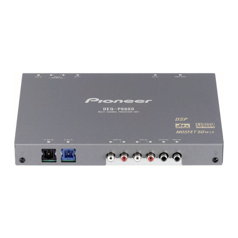
Pioneer DEQ-7200 User manual

W)
PIONEER’
The
Art
of
Entertainment
Service
_
ORDER.NO.
CRT1701
CONTENTS
4.
SPECIFICATIONS......--essececseeees
eee
eT
Rn,
2
2.
OPERATIONS
AND
CONNECTION
......cesccesecesceeeares
ce
3.
DISASSEMBLY
.......cecescccssccocececsecesssesessseessceaterecencers
10
4,
ELECTRICAL
PARTS
LIST
..csccscssccsesscssssesseceeeseseeseee
15
5.
CIRCUIT
DIAGRAM
AND
PATTERN
.......00.esseeeeeeee
17
6.
BLOCK
DIAGRAM
......eescccccsscesssceccsssecesercentenesscescees
25
7.
EXPLODED
VIEW
........
Pddleatiraeteiera
tends
iedesuuatnees
26
8.
PACKING
METHOD
00...
cccscscccecececcececsccecccaveeseecnececsees
28
PIONEER
ELECTRONIC
CORPORATION
4-1,
Meguro
1-Chome,
Meguro-ku,
Tokyo
153,
Japan
PIONEER
ELECTRONICS
SERVICE,
INC.
P.O.Box
1760,
Long
Beach,
CA
90801-1760,
U.S.A.
PIONEER
ELECTRONIC
[EUROPE]
N.V.
Haven
1087
Keetberglaan
1,
9120
Melsele,
Betgium
PIONEER
ELECTRONICS
ASIACENTRE
PTE.LTD.
501
Orchard
Road,
#10-00
Lane
Crawford
Place,
Singapore
0923.
©
PIONEER
ELECTRONIC
CORPORATION
1995
|
K-FFU.MAY
1995
rrintea
in
vapan

3IEG-7200
SAFETY
INFORMATION
(UC
MODEL)
CAUTION
This
service
manual
is
intended
for
qualified
service
technicians;
it
is
not
meant
for
the
casual
do-it-yourselfer.
Qualified
technicians
have
the
necessary
test
equipment
and
tools,
and
have
been
trained
to
properly
and
safely
repair
complex
products
such
as
those
covered
by
this
manual.
Improperly
performed
repairs
can
adversely
affect
the
safety
and
reliability
of
the
product
and
may
void
the
warranty.
If
you
are
not
qualified
to
perform
the
repair
of
this
product
properly
and
safely;
you
should
not
risk
trying
to
do
so
and
refer
the
repair
to
a
qualified
service
technician.
WARNING
Lead
in
solder
uséd
in
this
product
is
listed
by
the
California
Health
and
Welfare
agency
as
a
known
reproductive
toxicant
which
may
cause
birth
defects
or
other
reproductive
harm
(California
Heaith.&
Safety
Code,
Section
25249.5).
When
servicing
or
handling
circuit
boards
and
other
components
which
contain
lead
in
solder,
avoid
unprotected
skin
contact
with
the
solder.
Also,
when
soldering
do
not
inhale
any
smoke
or
fumes
produced.
1.
SPECIFICATIONS
General
Equalizer
POWESL
SOUICE
0...
...ceccseseeeecereeesewes
14.4
V
DC
(10.8
—
15.6
V
allowable)
Equalizing
frequencies.
GrOUNGING
SY
SCI
secscencscaccewsn
cckiveadevavsecbadsdneseousnaszenendevess
Negative
type
(15-band
graphic
equalizer)
..........eceeseceeeeee
teens
25
Hz,
40
Hz,
63
Hz,
Dimensions
100
Hz,
160
Hz,
250
Hz,
400
Hz,
(DIN)
(mounting
Size)
............
eee
178
(W)
x
50
(H)
x
132
(BD)
mm
630
Hz,
1
kHz,
1.6
kHz,
2.5
kHz,
(WNOSG)
csdusasinvatsevancces
estan
oeens
188
(W)
x
58
(H)
x
17
(D)
mm
4
kHz,
6.3
kHz,
10
kHz,
16
kHz
(D)
(mounting
size)
.....
ee
178
{(W)
x
50
{H)
x
137
(1D)
mm
Equalization
PIAS
a
sacsscctuscerdaccctseaexsuee
heacanahebanvenssaendeveccesseeteoees
+12
dB
(MOSE)
-eeeesesceerecereseeten
sence
cseeenees
170
(W)
x
46
(H}
x
12
(D)
mm
DUSTOMMONN
piacidecccccaactelstichissaveatseucs
0.01%
(1
kHz,
500
mV,
20
kHz
LPF)
Weight
be
a
a
lia
ste
rte
Maat
rae
Seas
tea
anata
ithe
Seu
bl
cbaban
0.6
kg
FreQUeNCy
FOSPONSE
..........seccesecesseenseserensenes
20
—
20,000
Hz
(0,
-1
dB)
|
Signal-to-noise
ratio
..........cscceesscccesesseessestensenes
85
dB
(IEC-A
network)
Input
level/IMPeMANCe
...........ccccescsseeecsrcescesssereesensenssnenees
500
mV/22
kQ
Output
level/impPGA
ane
:iviccccs-.sesccscessscicspecesesnteseaseacecdeeeas
500
mV/1
kQ
Maximum
output
level
sasnsccseucavessssconcsncsvendvocscrese
1.5
V/1
kHz,
1%
THD
Note:
Specifications
and
the
design
are
subject
to
possible
modification
without
notice
due
to
improvements.
2.
OPERATIONS
AND
CONNECTION
Precautions
|
In
case
of
trouble
|
When
the
unit
dose
not
operate
properly,
contact
your
dealer
or
the
nearest
authorized
PIONEER
Service
Station.
Never
remove
the
top
case
of
the
unit
to
attempt
check
or
repairs.
Memory
Backup
When
the
car
battery
is
removed
or
power
cord
of
this
unit
is
disconnected,
and
the
power
is
not
supplied
for
about
3
days,
the
settings
of
the
position
and
equalizer
curves,
etc.
are
initialized.
Connecting
the
Units
Note:
*
This
unit
is
for
vehicles
with
a
12-volt
battery
and
negative
grounding.
Before
installing
it
in
a
recreational
vehicle,
truck,
or
bus,
check
the
battery
voltage.
*
To
avoid
shorts
in
the
electrical
system,
be
sure
to
disconnect
the
battery
©
cable
before
beginning
installation.
*
Refer
to
the
owner's
manual
for
details
on
connecting
the
power
amp
and
other
units,
then
make
connections
correctly.
«
Secure
the
wiring
with
cable
clamps
or
adhesive
tape.
To
protect
the
wiring,
wrap
adhesive
tape
around
them
where
they
lie
against
metal
parts.
«
Route
and
secure
all
wiring
so
it
cannot
touch
any
moving
parts,
such
as
the
gear
shift,
handbrake,
and
seat
rails.
Do
not
route
wiring
in
places
that
get
hot,
such
as
near
the
heater
outlet.
If
the
insulation
of
the
wiring
melts
or
gets
torn,
there
is
a
danger
of
the
wiring
short-circuiting
to
the
vehicle
body.
-
Don’t
pass
the
orange
lead
through
a
hole
into
the
engine
compartment
to
connect
to
the
battery.
This
will
damage
the
lead
insulation
and
cause
a
very
dangerous
short.
:
*
Donot
shorten
any
leads.
If
you
do,
the
protection
circuit
may
fail
to
work
when
it
should.
DEG-7200
Never
feed
power
to
other
equipment
by
cutting
the
insulation
of
the
power
supply
lead
of
the
unit
and
tapping
into
the
lead.
The
current
capacity
of
the
lead
will
be
exceeded,
causing
over
heating.
When
replacing
fuse,
be
sure
to
use
only
fuse
of
the
rating
prescribed
on
the
fuse
holder.
;
When
the
2-speaker
system
is
employed,
use
the
front
outputs
of
this
unit.
Otherwise,
the
effects
of
the
sound
field
control
cannot
be
obtained.
Connection
Diagram
(Connecting
to
a
head
unit
having
front
and
rear
inputs)
(Fig.
1)
4.
Rear
output
2.
Front
output
3.
External
input
4.
Connecting
cord
with
RCA
pin
plugs
(sold
separately)
Connect
red
to
red
and
white
to
white.
5.
External
(audio)
output
6.
Front
input
7.
Rear
input
8.
Head
unit
(Ex.
KEH-P9250)
In
this
connection,
the
MAIN
IN
switch
in
the
head
unit
should
be
set
to
ON.
9.
Blue
To
system
contro!
terminals
of
the
head
unit.
10.
Blue
11.
Front
speakers
12.
Rear
speakers
13.
Black
(ground)
To
vehicle
(metal)
body.
14.
Yellow
To
lighting
switch
terminal.
15.
Orange
;
To
terminal
always
supplied
with
power
regardiess
of
ignition
switch
position.
16.
Fuse
resistor
17.
Fuse
holder
Fig.
1

DEQ-7200
Connection
Diagram
.
(Connecting
to
a
head
unit
which
does
not
have
Troni
and
rear
inputs)
(Fig.
2)
1.
Rear
output
|
2.
Front
output
3.
External
input
4.
Connecting
cord
with
RCA
pin
plugs
(sold
separately)
Connect
red
to
red
and
white
to
white.
5.
Rear
output
6.
Front
output
Not
used
in
this
connectton.
7.
Sub-woofer
output
Not
used
in
this
connection.
8.
Head
unit
(Ex.
KEH-P8250).
9,
Blue
To
system
contro}
terminals
of
the
head
unit
and
power
amp.
10.
Blue
11.
Power
amp
(sold
separately)
12.
Front
speakers
13.
Rear
speakers
14.
Black
(ground)
To
vehicle
(metal)
body.
15.
Yellow
To
lighting
switch
terminal.
16.
Orange
To
terminal
always
supplied
with
power
regardiess
of
ignition
switch
position.
17.
Fuse
resistor
.
18.
Fuse
holder
[11]
[10]
[9]
[3]
[7]
[6]
Fig.
3
Fig.
2
[14]
[15]
[18]
[17][16]
Fig.
4
A
arr
lrni

i
ze
Bageneie
9
Using
the
Clear
Button
Pressing
the
Clear
button
will
reset
the
microprocessor.
Press
the
Clear
button
in
the
following
cases:
»
When
using
the
unit
for
the
first
time
after
connecting
it.
¢«
When
there
is
a
misoperation.
«
When
the
display
indicates
a
misoperation.
Press
the
Clear
button
with
the
tip
of
a
pen,
etc.
(Fig.
5).
Clear
button
Fig.
5
Demo
Mode
When
the
audio
signal
is
not
input
for
more
than
20
seconds,
the
display
automatically
switches.to
the
demo
mode.
The
dispaly
is
restored
when
an
audio
signal
is
input
to
this
unit.
.
Changing
the
Spectrum
Analyzer
Display
Parts
Identification
Fig.
3
[3]
Display
[11]
Spectrum
analyzer
display
selector
‘button
Fig.
4
[13]
Operation
display
Each
time
button
[11]
is
pressed,
the
operation
display
[13]
changes
in
the
sequence
from
A,
B,
C,
D,
E
then
F.
A:
Peak
Bound
Display
This
indicates
the
music
energy
level
of
each
frequency
by
the
height
of
the bar
for
each
band,
while
also
showing
a
temporary
indication
of
level
peaks.
B:
Symmetric
Display
|
This
indicates
the
music
energy
level
of
each
frequency
by
width.
Setting
the
Head
nit
Parts
Identification
Fig.
3
[1]
Volume
buttons
[3]
Display
Fig.
4
[17]
Sound
clip
indicator’
When
this
unit
is
connected
to
the
head
unit,
the
volume,
balance
and
fader
can
be
adjusted
with
this
unit.
Before
operating
this
unit,
set
the
head
unit
as
follows.
1.
Press
the
(-)
side
of
buttons
[1]
to
set
the
volume
of
the
unit
to
“VOL
0”.
2.
Set
the
volume
of
the
head
unit
to
“VOL
23":
3.
Set
the
fader
and
balance
of
the
head
unit
to
center
position.
«
To
adjust
the
volume,
fader
and
balance
on
the
head
unit,
refer
to
the
Owner's
Manual
that
accompanies
the
head
unit.
DEQG-7200
C:
Peak
Display
This
indicates
the
music
energy
level
of
each
frequency
by
the
height
of
the
bar
for
each
band.
D:
Radial
Display
The
sound
intensity
is
displayed
in
a
radial
shape.
E:
Winding
Road
Display
This
displays
an
image
giving
the
impression
of
traveling
along
a
winding
road.
Speed
changes
depending
on
the
music
energy
level.
F:
Graphic
Equalizer
Display
The
current
equalizer
curve
is
displayed.
ee
When
the
head
unit
volume
is
excessive
(excessive
input
to
the
unit),
“CLIP”
[17]
will
be
indicated
on
the
display
as
a
‘warning.
In
this
case,
turn
the
volume
—
on
the
head
unit
down
to
the
point
where
“CLIP”
is
no
longer
displayed.
-
When
you
feel
a
distortion
in
the
sound
even
though
“CLIP”
is
not
indicated
on
the
display,
turn
the
volume
on
the
head
unit
down.
*
The
volume’s
set
point
is
not
indicated
on
the
display
when
you
adjust
the
volume
on
the
head
unit
by
tuning
the
volume
control.
In
this
case,
set
the
volume
control
on
the
head
unit
to
the
position
illustrated
below,
in
accordance
with
step
2.
(Fig.
6)
ae
Adjusting
range
MIN
MAX
Fig.
6

DEQG-7200
Adjusting
the
Volume
Parts
identification
Fig.
3
{1}
Volume
buttons
[3]
Display
Fig.4
|
{15}
Numeric
display
Pressing
the
(+)
side
of
buttons
[1]
increases
the
volume,
while
the
(—}
side
of
|
buttons
[1]
decreases
it.
(Numeric
display
[15]
shows
"VOL
0
—
VOL
30".)
Note:
*
Always
keep
the
volume
inside
the
car
at
a
level
that
allows
you
to
hear
outside
sounds.
Fine
tuning
of
the
Position
(Fader/Balance)
After
choosing
the
position
using
the
.
position
selector
function,
it
is
possible
to
fine
tune
the
sound
image
positioning
by
adjusting
the
fader
and
balance
controls.
+
The
fine
tuning
can
be
applied
independently
for
each
position.
*
The
condition
after
fine
tuning
will
be
stored
in
memory
as
the
setting
for
each
position.
The
next
time
the
position
is
recalled,
the
setting
after
fine
tuning
will
be
recalled.
1.
Press
button
[4]
to
switch
to
the
fader/
—
‘balance
mode.
._.
Each
press
of
button
changes
the
mode
as
shown
below.
Fader/balance
modé.
Nuance
contro!
mode
Graphic
equalizer
mode
Adjusting
the
Listening
Position
One
of
the
conditions
for
reproduction
of
more
natural
music
is
to
“clearly
define
the
sound
image
positioning
(listen
to
music
at
the
center
of
the
sound
field)”.
The
position
selector
function
appropriately
adjusts
the
delay
time
and
level
of
the
sound
from
each
speaker
according
to
the
seat
position(s)
and
the
number
of
people
in
the
car
and
allows
to
recall
this
setting
with
a
single
button
operation.
This
makes
the
listener(s)
possible
to
obtain
natural
acoustic
property
regardless
of
the
seat
positions.
Parts
Identification
Fig.
3
[3]
Display
[4]
Mode
shift
button
{5)
Fader
control
buttons
{6]
Balance
control
buttons
{7]
Position
selector
button
Fig.
4
[13]
Operation
dispiay
[15]
Numeric
display
[16]
Position
indicator
2.
Press
(A)
or
(W)
side
of
buttons
[5]
to
adjust
the
volume
balance
between
the
front
and
rear
(fader
control).
(Numeric
display
[15]
shows
"F25
—
R25",)
|
:
3.
Press
(<4)
or
(>)
side
of
buttons
[6]
to
adjust
the
balance
between
the
left
and
right
(balance
control).
(Numeric
display
[15]
shows
“L25
—
R25".)
Setting
the
Listening
Position
(Position
selector)
Set
the
listening
position
according
to
the
position(s)
of
the
listener(s).
Press
button
[7].
Each
press
of
button
changes
the
listening
positions
[16]
as
follows.
OFF
Front/left
Front/right
oz
13;
ai
ob
(CH
aman
CC
Sy}
8
ALL
Front
Resetting
the
Position
The
sound
image
positioning
after
fine
tuning
can
be
reset
to
the
initial
conditions
_
of
the
fader
and
balance
control.
Press
and
hold
button
[7]
for
more
than
2
seconds.
.
a
A
short
beep
sound
is
generated
and
the
fader/balance
are
initialized.
*
Only
the
currently
selected
position
can
be
reset.
Note:
*
The
fader
control
is
not
used
with
a
2-
-
speaker
system.
Set
the
fader
to
the
center
position.
*
lf
your
system
is
configured
so
that
it
does
not-use
either
the
front.or
rear
output
of
this
unit,
the
position
selector
and
fader
will
not
function
properly.
‘If
you
system
is
a
4-speaker
system
which
is
configured
without
using
either
the
front
or
rear
output
of
this
unit,
the
volume
balance
between
the
front
and
rear
speakers
should
be
adjusted
on
the
nead
unit.

Adjusting
the
Equalizer
Curve
Parts
Identification
Fig.
3
[3]
Display
[4]
Mode
shift
button
[5]
Nuance
control
up/down
buttons
Level
up/down
buttons
[6]
Frequency
up/down
buttons
{8}
Speaker
selector
button
[9]
User’s
curve
memory
buttons
{10}
Factory
preset
curve
buttons
Fig.
4
{13]
Operation
display
{14]
Nuance
control
indicator
{15]
Numeric
display
{19}]
User’s
curve
memory
indicators
[20]
Factory
preset
curve
indicators
VOCAL
(F3)
|
Emphasizes
the
portion
of
the
voice
band
and
minimizes
the
low-range
to
increase
articulation.
Use
this
mode
to
emphasize
vocal
signals
or
when
listening
to
conversation.
JAZZ
(F4)
|
Compared
with
ROCK
mode,
emphasizes
the
low-
and
high-ranges
more
intensively
so
the
wide-range
feeling
can
be
obtained.
Suitable
to
enjoy
jazz
music
in
a
relaxed
environment.
Selecting
the
speakers
to
be
Equalized
Select
the
speakers
to
which
the
equalizer
effect
is
applied,
from
the
front,
rear
or
both.
Press
button
[8].
Each
press
of
button
changes
the
speakers
affected
by
the
equalizer
as
shown
below.
pevre
ete
7
ON:
The
frame
is
displayed.
OFF:
The
frame
is
not
displayed.
(F}
®
Both
front/rear
speakers
Front
speakers
only
Rear
speakers
only
Recalling
a
Factory
Curve
Press
one
of
(F1)
to
(F4)
buttons
[19]
to
select
the
factory
curve
to
be
recalled.
(The
display
frame
[20]
of
the
selected
|
factory
curve
lights.)
DEQ-7200
Equalizer
Curve
Recall
Four
equalizer
curves
have
been
preset
in
memory
(factory
curves}
to
allow
pegine
with
simple
operation.
Factory
Preset
Curves
|
The
4
factory
curves
have
been
preset
in
the
memory.
ROCK
(F1}
Focuses
on
the
band
of
rhythm
section
of
rock
music
so
that
powerful
sound
can
be
reproduced
with
supplemented
low
and
high
ranges.
POPS
(F2)
Particularly
emphasizes
the
middle-range
so
that
light
pops
sound
can
be
enjoyed.
Adjusting
the
Equalizer
Curve
The
equalizer
curve
can
be
adjusted
i
in
the
following
2
ways.
Nuance
control
Overall
adjustment
of
the
effect
of
equalizer
curve
(nuance
control)
is
possible.
15-band
graphic
equalizer
adjustment
The
level
of
each
of
the
15
bands
(at
2/3
octave
intervals)
can
be
adjusted.
Nuance
Control.
1.
Press
button
[4]
to
switch
to
the
nuance
control
mode.
Each
press
of
button
changes
the
mode
as
shown
below.
Fader/balance
mode
v
Nuance
control
mode
(Example:
ROCK
(F1)}
Graphic
equalizer
mode

DEG-7200
2.
Recall
the
equalizer
curve
to
be
adjusted.
Recail
a
factory
curve
or
user’s
Curve
(equalizer
curve
created
and
stored
in
this
unit
by
yourself).
(Refer
to
“Recalling
a
Factory
Curve”
on
page
7
and
“Recalling
a
User's
Curve”
.)
*
Auser’s
curve
in
which
no
equalizer
curve
has
been
set
(=
flat
curve)
cannot
be
adjusted
with
nuance
control.
3.
Press
(A).or
(¥)
side
of
buttons
[5]
to
apply
nuance
control.
Pressing
the
(A)
side
increases
the
amount
of
compensation
(increases
the
difference
between
high
and
low
levels.)
Pressing
the
(W)
side
decreases
the
.
amount
of
compensation
(towards
flat.)
(Numeric
display
shows
"—6
—
6".)
+
The
nuance
control
can
be
applied
separately
to
the
factory
curves
and
user’s
curves.
*
The
condition
after
nuance
control
of
each
factor
curve
or
user’s
curve
is
stored
as
the
setting
value
for
than
curve.
The
next
time
the
factory
curve
or
user’s
curve
is
recalled,
the
equalizer
|
curve
after
nuance
contro!
will
be
recalled.
Storing
Equalizer
Curves
The
equalizer
curves
adjusted
by
the
user
can
be
stored
as
the
user’s
curves
in
the
memory
under
4
buttons
[9].
Storing
a
User’s
Curve
in
Memory
1.
Adjust
an
equalizer
curve
as
desired.
(Refer
to
“Adjusting
the
Equalizer
Curve”
on
page
7.)
2.
Press
and
hold
one
of
(U1)
to
(U4)
of
buttons
[9]
that
you
want
to
store
the
equalizer
curve
for
more
than
2
seconds.
{The
frame
of
the
“USER
1—
USER
4”
indicators
[19]
corresponding
to
the
pressed
button
[9]
blinks
during
storing
and
lights
up
after
completion
of.
storing.)
¢
If
an
equalizer
curve
has
aiready
been
‘stored
under
the
button,
the
previous
memory
is
cleared
and
the
new
equalizer
curve
is
stored
in
memory.
«
When
a
equalizer
curve
is
stored,
its
nuance
control
value
is
set
to
0.
15-Band
Graphic
Equalizer
Adjustment
1.
Press
button
[4]
to
switch
to
the
graphic
equalizer
mode.
Each
press
of
button
changes
the
mode
as
shown
below.
Fader/balance
mode
Vv
Nuance
control
mode
v
Graphic
equalizer
mode
(Example:
ROCK
(F1))
2.
Recall
the
equalizer
curve
to
be
adjusted.
Recall
a
factory
curve
or
user’s
curve
(equalizer
curve
created
and
stored
in
this
unit
by
yourself).
.
(Refer
to-“Recalling
a
Factory
Curve”
on
page
7
and
“Recalling
a
User’s
Curve”
.)
Recalling
a
User’s
Curve
The
equalizer
curves
stored
under
buttons
[9]
(user's
curves)
can
be
recalled
as
required.
Press
one
of
(U1)
to
(U4)
of
buttons
19]
that
store
the
user’s
curves
to
be
recalled.
(The
display
frame
[19]
of
the
selected
user’s
curve
lights.)
3.
Press
(<4)
or
(»)
side
of
buttons
[6]
to
select
the
frequency
to
be
adjusted.
25
Hz
to
16
kHz
(2/3
octave/step)
4.
Press
(A)
or
(¥)
side
of
buttons
[5]
to
adjust
the
level.
(Numeric
display
[15]
shows
"-6
—
6".)}
5.
Adjust
other
frequency
bands
by
repeating
steps
3
and
4
for
each
of
them.
6.
Store
the
adjusted
equalizer
curve
in
memory.
The
adjusted
equalizer
curve
will
be
reset
when
another
equalizer
curve
is
recalied.
tf
you
want
to
retain
the
adjusted
curve,
store
it
in
the
memory
of
this
unit.
(Refer
to
“Storing
Equalizer
Curves”
.)
Flat
Curve
Function
An
equalizer
can
be
reset
to
a
flat
curve
with
asimple
operation.
Press
and
hold
one
of
{F1)
to
(F4)
of
buttons
[10]
for
more
than
2
seconds.
The
graphic
equalizer
mode
is
initiated
and
the
corresponding
equalizer
curve
is
made
flat.
ere

Sound
Field
Control
Function
The
sound
field
control
(SFC)
function
provides
programs
reproducing
3
typical
sound
field
spaces
of
a
studio,
club
and
live
house.
The
SFC
makes
it
possible
to
reproduce
a
realistic
sound
field
in
the
car
compartment
as
if
the
listener(s)
are
actually
present
in
that
space.
Using
the
Remote
Control
When
the
DSP/MAIN
UNIT
switch
in
the
remote
controller
supplied
with
head
unit
is
set
to
“DSP”,
some
functions
of
this
unit
can
be
performed
with
the
remote
.
controller.
*
The
volume
buttons
and
the
attenuator
button
operate
this
unit
directly
and
do
not
operate
the
head
unit.
(The
volume
level
of
the
head
unit
can
be
adjusted
with
the
volume
buttons
in
the
head
unit.)
¢
Some
functions
of
this
unit
can
be
:
-
operated
with
the
DSP
button.
Fig.
7
Sound
Field
Programs
Preset
in
this
Unit
The
following
3
sound
field
programs
are
preset.
STUDIO
Localizes
the
sound
image
to
the
axial
sensitivity
and
does
not
add
reverberation
sound.
Reproduces
basic
sound
field
by
processing
initial
reflection
sound
from
the
walls
of
a
relatively
small
mixing
room.
CLUB
Reproduces
music
performed
in
discos
for
about
50
people.
Suitable
for
reproducing
a
sound
field
with
facilitated
absorption
of
reverberation
and
enjoying
music
with
powerful
beat.
LIVE
HOUSE
Reproduces
music
performed
in
a
live
house
for
50
to
100
audiences.
Highly
effective
for
sound
sources
such
as
recorded
gigs.
Provides
real
reproduction
of
reflection
from
the
walls
and
reverberation.
Parts
Identification
and
Function
—
Fig.
8
Parts
Identification
Fig.
3
Or
Sound
field
control
button
[3]
Display
Fig.
4
[12]
Sound
field
control
indicators
Recalling
a
Sound
Field
Program
Press
button
[2]
to
select
the
desired
sound
field
program.
Each
press
of
button
recalls
the
sound
field
program
in
the
order
of
STUDIO
~
CLUB
>
LIVE
HOUSE
~@
SFC
OFF
STUDIO...
(The
display
frame
[12]
of
the
recalled
sound
field
program
lights.)
(When
the
SFC
is
OFF,
all
frames
[12]
go
off.)
;
{21]
Volume
buttons
Press
the
(+)
side
to
increase
volume
and
the
(-)
side
to
decrease
volume.
{22]
DSP
button
Except
when
the
user's
curve
is
being
recalled:
Used
to
recall
factory
preset
equalizer
curve.
Each
time
the
button
is
pressed,
the
selected
factory
preset
equalizer
curve
changes
in
the
sequence
of
ROCK
>
POPS
>
VOCAL
2
JAZZ
>
ROCK...
|
When
the
user's
curve
is
being
recalled:
Used
to
recall
the
user's
curve.
Each
time
the
button
is
pressed,
the
selected
user's
_curve
changes
in
the
sequence
of
USER
1
>
USER
2
USER
3%
USER
42
USER
1....
[23]
Attenuator
button
Press
to
reduce
the
volume
to
1/10
of
its
current
setting
(
“ATT”
is
cieplaye’
in
the
operation
display
[13].)
Pressing
again
returns
the
volume
to
its
original
level.
This
function
is
available
using
the
remote
controller
unit
only.

DEQ-7200
3.
DISASSEMBLY
@
Removing
the
Case
and
Grille
Assy
__
@
Removing
the
Audio
Unit
|
1.Removing
the
case.(not
shown)
|
1.Unbend
the
tabs
at
location
indicated
by
arrows
2.Removing
the
connector.
|
until
straight.
3.Disconnect
the
four
stoppers
indicated
by
arrows.
7
2.Removing
the
audio
unit.
4.Removing
the
grille
assy.
Grille
Assy
|
Fig.9
Fig.10
@
ICs
LC7582EMT
|
~
RS-30
BOTTOM
VIEW
$1
$2
$3
$4
SB
$6
S7
$8
s9
-
$10
$11
$12
$13
$14
$15
$16
s
[>>
ist
AMP
LIMITER
OUT
410

DEG-7200
~
@
Pin
Functions
(AK5340-VS)
PT
AINE
ch
analognon-invertinginput)
p
2
CUT
AINE
ST
LCi
ch
analoginvertinginput,
ee
—s—sSSSCSsS
|
3
sd|
VREFIN§
[1
=|
Referencevoltageinput)
rr
s—“—s—Cs—“‘“‘“‘“‘SCSs
4
AC
Powersupply(+5V)
foranalogcircuit
p56
UL
AGND
UT
Cs
GND
for
analog
circuit
|
Pace
SO
or
ING
ele
ee
et
eee
et
ee
eee
emg
|
8
dt
tst1
|
Cs
Test
pin(open)
|
|
9
=|
SELIG,
=|
|
CC*d|«Quitputdatalengthselect
Cs
|
10
|
PDC
|
Power
down
pin
| _
Pe
Pe
VO
Pe
asec
OBE
PIMGIND)
ne
ns
ee
|
12)
Cmobe
=O
|
Cd]
XMasterclockselect)
—
———“—‘Cs—‘“‘“‘“‘“‘“‘s*™SCSsY
|
13
~~}
SMODE
|| si
Interfaceclockselect_
—
—i(‘“‘“‘C™S™*™*~*~*™C™:C~*™r
Input
channel
select
_ |
|
16
SCE
SDATA
dT
OO)
™C—C—~—S
Seri
ddataoutput
er
—(—‘“<“‘“‘“‘sSOCSsS
|
17.
SYNC.
|.
VO.
Frame
synchronize
clock
|
|
18
=|
vop+
|
Ss
Powerr'Supply(+5V)fordigital
circuit
=
s—‘“C:sSC—sSY
|
19
|
DGND
|
—————sdsSCGGND
fr
digital
circuit
|
|
20,CldE
cK
CTCL
ss
Maater'clock
input
|
21,22
=|
TST34
~—|
SS
s=|s
Test
pin(open)
a
a
ee
|
24—si«dYsSVDB+—s—<‘iYL:Sti(istsSS
ss
Power
supp
ly(+5V)
for
digital
circuit
Ee
\
-
|
26
|
VREF
=
=|.O0
|
Reference
voltage
output
|
27)
AINR-
=
Le
sts&RRoch
analog
inverting
input
|
=—s2g-ti‘Ls«SAINARG
~=—sdE
dE
SSSS—sSYs&RRech
analog
non-inverting
input
AK5340-VS
AINR+
AINR-
VREF
NC
VDB+
TST4
TST3
CLK
DGND
VDP+
FSYNCSDATA
SCLK
'
xr
[20
[252
[23|
[2a
[2x20]
[19/017
[16][15
O
PY
ERAT
_—
—
a
i
ie
i
ey
err
aren
~
al
112
113
}14
[5
fle |L7
|e]
9
joj
11
ff
t2i[3
jit
R
AINL+
AINL-
VREFINVA+
AGND
NC
NC
TST1
SEL18
PD
TST2
ear
2
UR
:
| |
D
SERIAL
OUTPUT
INTERFACE
DECIMATION
at
|
rae
~}
m
J
Oe
enn
nn
ee
ee
ee
ee
eee
C
1
|
!
i
|
I
i
I
!
|
1
!
|
'
!
H
I
i
i
I
|
!
J
I
a
O
111

DEQ-7200
i
@
Pin
Functions
(PD5312A)
Pin
No.
VQ
|VOFormat
[Functionand
Operation
—
—“‘“C;*™*™*™*;*~*™
|
tC
|
1
|.
Clip.
sense
input
a
|
oe
DSPACK
|
|
|
~~
—*([AcknowledgeinputfromDSPIC
=
™~—“SCSCCS
|
4
|
psPpcD
|
O
|
C
|AddressoutputforDSPIC
—————COC
tL
5
|
DPD
|
oO
|
C
[Calibration
output
for
DSP
IC
eo
ama
6
|
PEED
CUT
OF
UT
CC
i
Beep
tone
output
eas
|
ee
tte
{L7
|
bspcs
|
Oo
|
C
[ChipselectoutputforDSPIC
SSS
O™~S
|
8
|
DsPRST
|
O
|
CC
[ResetoutputforDSPIC
|.
——~—~CSCS
|
9
=|
DSPCK
|
O
|
C
[SerialclockoutputforDSPIC
——Ssss—~CS;
}XETCS*«*
|
10~=©|)«636DSPOUT
| O |
C
{Serial
data
output
for
DSP
IC
|
|
it
|
ODSPIN
|
1
|
C
{Serial
data
input
from
DSP
IC
| |
=
Serial
clock
output
for
LCD
driver
|
|
14
|
DT
|
OO
CT
CC
DatacoutputforLCDdriver—“—S™~™SCSOCOOOOOOCOCOCOCS
15,16
|
LCE12
|
O
|
C
[Chipenable
outputpinforLCDdrive
t—~sS
|
17
|
REMIN,
|
|
|
[Remote
controlsignalinput——“—sS™S™~™~™C™COCOOCOOOOOC~CS
Peete
1
CNWSS
so
le
GND
ee
ee
RESET
=|
||
SCC
Reset
input
BSEN
|
|
|
si
Back
up-power
sense
input
=
ons
ts
see
|
|
SysB
|
1
|
~~
[System
remote
control
input
22
Crystal
oscillating
element
connection
pin
Crystal
oscillating
element
connection
pin
Position
select
input
Model
select
input
XOQUT
25
POSL
26
2]
P
|
Notused
__C
C
_C
E
29
31
i
Strobe
pulse
output
for
electronic
volume
Data
output
for
electronic
volume
(fumination
power
ON/OFF
out
Not
used
D
converter
power
ON/OFF
output
jis
alslS|
OO
Zia
yvi<|x|x
NOAM
eA
<iAaDloimlolsS
AIA
DUO
awl
ay
inion
Z2\a\m|
Diz
|
Z|
j2ic
G9
|
Go
700
|
Co
.¢)
NO
ROTRO
Ro
01)
/Go/
ho
©
ie
*)
fico
a
36
37-55
56
57
ve
2
|
D
converter
reference
voltage
D
converter
GND
ey
data
input
AVSS
2
|
KDT0-3
60-63
Zz
Jo
Pl
Zit
CO
AID
Oiow
|
za
hed
|
*PD5312A
‘0
Format
CMOS
|
_.
—l€"s-marked
by*.are-MOS
S33
|
Be
careful
in
handling
them
because
they
are
ee
very
liable
to
be
damaged
by
electrostatic
12

DEGQ-7200
@
Pin
Functions
(PD2038C)
0
go
de@t
eof
PO...
20)
1
Test
Cate
Outta
|
4
|
VDD
||
Power
supply
terminal
forlogic
circuit
a
es
RE
IO
IC)
<0
eae
ee
a
eae
ore
eee,
|
6-11
|
TP5-0
|
O
|
Test
data
output
|
|
Cae
|
|
12
|
vvSSR_
|
|
GND
terminal
forinternaldelayRAM
|
13
|
DDR
|
|
~Power
supply
terminal
for
internaldelayRAM
A
ea
lee
So
ND
ee
re
oa
ee
ee
|
15-17,
|
SbdO20
|
O
|
Serialdataoutput
oo
p
ABO
1h
SDN
O25)
Serial
data
inpert
(
isy
o
a
e
ce
QUE
ee
OR
eee.
le
esl
UR
clock input
(is)
soe
a
ee
ee
|
27
|
WK
|
OO
|
Wordclockoutput,
|
22]
FS32_——
|
|
Bitclockoutput(32fs)
|
23
|
=
FS64
|
|
CBitclockoutput(64fs)
|
24
|
EBCO.
CUT
|
«CBitclockinput,
es
ee
ERO
le
We
2
UR
COCO
no
a
es
eh
|
|
28,29
|
ELRIVO
|
1
|
LRclockinputt
|
30.—O|
6SYNC.
|
ts
Synchronizing
signal
input
Power
suoply
terminal
for
logic
circuit
vstal
oscillating
element
connection
pin
or
external
clock
inp
Crystal
oscillating
element
connection
pin
31
SSRs
nC
Oo
©
S|
|
-
O
_
System
clock
select
input
stal
oscillation
mode
or
VCO
oscillation
mode
select
input
ata
output
from
phase
comparator
nalog
GND
w
pass
filter
amplifier
output
ow
pass
filter
amplifier
input
|
nalog
power
supply
|
est
terminal
O{iM1G)
z=
O
o
As
No
5
G2
109109
G21
W
(OW
|G
+
m7
WY
2°
N
RST
|
Reset
signal
input
terminal
|
cS
__-__—i|_i__'{
Chip
select
input
IFCD
|
1
|.
Command
or
data
select
input
from
DSP
controller
IFDI
|
Lt
|
Data
input
from
DSP
controller
| }
i
49
|
IFDO
|.
O-
|
DataoutputforDSP
controller
|
IFCK
|
|
|
-
Shift
clock
input
from
DSP
controller
Acknowledge
signal
output
for
DSP
controller
GND
|
Test
data
output
|
NJM2100M
13

DEG-7200
.
@
LCD
(CAW1287)
Ly
Vp
ty,
le
ty
{)
STN
A
Oye
\
IL
FP
UP
UP
aD
ae
Ue
ay
ey
ad
Hedy
by uy
dg
mm
Of:
StCANIERE
UNG
Hed)
|
ea
issna}
(Pry
sp
dp
gp
ay
ee
mu
Cy
tee
CCUM
LCM
EEE
it
fa
:
|
I}
1
wy
a
ny
T.
On
A
‘
pops
}'
vara)"
jazz
}
“see
7}
user
2?"
user
a }
ey
Samat
ee
Co
ee
jo
——
HOUSE
—
ROCK
1
LIVE
Wu
TP
chee
tp ee
de
pad
cba
ep
ap
ap
ep
ap
ap
ee
Ep
ap
typ
yp ap
tet
SEGMENT
-
COMMON
Fig.11

peenbietath
dae
cee
ete
wg
es
DEQ-7200
4.
ELECTRICAL
PARTS
LIST
r-o000
DU00DU
DUOUODND
PPfPHD
PNPP_PAP
Ol
=====Circuit
Symbol
&
No.
Part
Name=====
Part
No
s====Circuit
Symbol
&
No.
Part
Name=====
Part
No
——
CAPACITORS
R
921
924
RS1/10$104J
pie
859
860
CCSQCHO0S0D50
a
age
pea
aca
|
.
:
:
:
C
301
302
090
R
925
926
927.
928
RS1/10$103J
@
Parts
whose
parts
numbers
are
omitted
are
subject
to
being
not
supplied.
eee
ee
poe
CKSOYB473K50
B:
be6
ee
@
The
part
numbers
shown
below
indicate
chip
components.
C
304
312
522 523
527
CKSQYB104K
16
R
931
RS1/2S391J
C
305
317
524
CEAS220M10
Chip
Resistor
|
_
C
306
313
401
402
501
502
503
504 505
506
CEAS4R7M35
R
932
| :
RS1/2S391J5.
3
|
R
933
,
RS1/10S472J
RS
1/0SOOO/“,
RS
VOOSOOOS
C
310 318
407
408
573 623
701
702 703
706
CKSQYB103K50
R
934.
|
RS1/2S391J
.
.
C
319
321
CEAS220M10
R
935
.
RS1/10S473J
Chip
Capacitor
(except
for
CQS.....)
C
320 322 620
621
622
624
625
626
627
CCSQCH220J50
:
CKS
ia;
COS
CSZS
ie
C
403
404
CKSQYB473K50
CAPACITORS
C
405
CSZSC100M16
|
sa===Circuit
Symbol
&
No.
Part
Name=s====
Part
No
se===Circuit
Symbol
&
No.
Part
Name=====
Part
No
C
406
861
862
CKSOYB103K50
:
oe
oc
ae
eget
a
eel
I
CO
a
a
a
Ae
A
Ta
a
C
511
512
513 514
515
516
853
854
857
858
CEAS4R7M35
C
905
CSZSR
100M6R3
Unit
Number
:
CWM4260(UC)
EF
951
CCG
1006
C
521
CKSQYB103K25
C
906
CKSQYB103K50
CWM4264(ES)
BZ
601
CPV1011
C
525
601
CEAS2R2M50
C
9807
908
S$ZS010M16
Unit
Name
—_:
Audio
Unit
|
C
526
553
554
563
10uF/16V
CCH1190
RESISTORS
MISCELLANEOUS
C
551
552
561
562
CCSQCH151550
R
301
302
303 304
311
312
313
314
RS
1/10S222J
C
555
556
565
566
CKSQYB102K50
IC
302
312
TC9268F
R
305
306
315
316
703
861
862
RS1/10S104J
C
564
572
574
604
10nF/16V
CCH1190
IC
303
313
TA2028F
R
321
576
RS1/10SOROJ
C
571
958
100uF/16V
CCH1191
IC
401
AK5340-VS
R
401
712
RS1/10SOROJ
C
605
CCSGQCH101J50
IC
501
PMJ003A
R
402
404
711
RS1/10SOROJ
iC
551
561
851
852
NJM4558MD
C
606
707
871
10uF/16V
CCH1190
R
403
603
608
611
616
617
618
619
620
622
RS1/10S102J
C
610
611
612
613
|
CCSQCH100J50
iC
601
PD5312A
R
501
|
RS1/10S152J
C
704
CKSQYB391K50
IC
602
(S-80722AN-DK-l)
GGC1040
R
502
503
504
RS1/10S302J
C
705
CKSYB684K
16
IC
701
PD2038C
R
551
552
561
562
885
886
RS1/10S104J
C
708
CEAS330M16
IC
702
TC74HC393AF
R
553
554
563
564
RS1/10S153J
IC
703
TC74HC175AF
C
709
879
961
CEAS470M16
R
555
556
565
566
RS1/10S123J
C
851
852
CEAS010M50
IC
704
TC7S04F
R
557
558
567
568
RS1/10S821J
C
855
856
CEAS4R7M35
IC
853
NJM2100M
R
559
560
569 570
577
RS
1/10S223J
C
863
864
CEAS4R7M35
IC
854
M5233FP
R
571
955
RS1/10S471J
C
865
866
CCSQCH120J50
IC
952
NJM78M05A
R
572
RS1/10S561J
:
Q
551
552
561
562
DTC314TK
C
867
868
CKSQYB332K50
R
573
RS1/10S223J
C
869
881
882
220nF/10V
CCH1193
571
956
958
960
963
2SC2412K
R
574
621
629
887
888
952
971
RS1/10S473J
C
870
877
883
884
956
957 959
960
963
~
CKSQYB103K50
572 604 954
962
DTC124EK
R
575
865
866
953
959
)
RS1/10S472J
C
872
873
874
878
10uF/16V
CCH1190
573
601
DTA124EK
R
601
609
623 625
RS1/10S102J
C
885
886
,
CEA4R7M35NPLL
602 603
952
—
DTC124EK
R
602
RS1/108124J
605
FMG5
|
C
951
968
1000.F/16V
CCH1185
|
R
604
605
607
954 956
958 960
961
962
RS
1/108473J
C
953
|
CKSYB105K16
851
852
2SC2412K
R
612
613
|
RS1/10S101J
C
954
955
964
965
10yF/16V
©
CCH1190
951
|
2$B1243
R
614
615
702.
|
a
feet
~-RS1/10S101J
CC
92
0°
©
0.22F/5.5V
CCL1037
953
964
2SA1037K
R
624
626
627
628
713
714
883
884
969
RS1/10S102J
C
966
970
10,
F/16V
CCH1190
955
957 965
2SD1760F5
R
630
RS1/10S103J
|
959
2SA1797
Unit
Number
:
CWS1290(UC)
|
R
701
|
RS
1/10S562J
CWS1291(ES)
966
2SD1864
R
715
716
721
963
RS1/10S103J
Unit
Name
__:
Key
Board
Unit
571
601
|
MA151K-MH
~R
720
873 874
879
RS
1/10S103J
572
DTZ8R2B
R
851
852
857
858
859
860
957
RS
1/10S223J
MISCELLANEOUS
951
ERA15-02VH
R
853
854
RS1/10S114J
952
960
MA3082L
IC
901
902
LC7582EMT
7
R
855
856
RS1/10S154J
IC
903
RS-30
953
MA151K-MH
R
863
864
RS1/10S224J
Q
901
-
28C2412K
954
|
MA3091L
R
867
868
877
878
974
977
RS1/10S472J
D
901
902
903
904
ChipLED
CL170FGCD
955
|
|
DTZ7R5C
R
869 870
RS
1/10S563J
D
905 906 907
908
ChipLED
CL170FGCD
956
—
|
|
SC016-2
R
871
872
RS1/10S154J
|
)
957
DTZ6R2C
D
909
910
911
Chip
LED
CL170FGCD
|
R
875
876
RS
1/10S331J
D
912
|
:
MA30621
958
MA151WK
R
880
ks
RS1/10S153J
S
901
902
903
904
Switch
CSG1041
959
MA3047M
R
881
882
RS1/10S151J
S
905
906
907 908
Switch
CSG1041
961
:
MA151K
-
R
964
970 975
976
983
RS1/10S473J
S
909
910
911
912
Switch
CSG1041
971
972
MA8180M
R
965
RS1/4S102J
301
302
303
311
Ferri-Inductor
LAU2R2K
.
S
913
914
915
916
Switch
CSG1041
R
966
982
-
RS
1/2S180J
S
917
918
919
920
Switch
CSG1041
L
312
313
401
601
_
Ferri-Inductor
LAU2R2K
R
967
RS1/10S512J
IL
901
902
Lamp
14V
40mA
CEL1436
L
702
703
Ferri-Inductor
LAU2R2K
R
968
RS1/10S241J
LCD901
LCD
CAW
1287
L
559
560
561
Inductor
LCTB2R2K2125
R
972
RS
1/4S472J
L
569
570
571
Inductor
LCTB2R2K2125
R
973
RS1/10S101J
RESISTORS
L
701
Ferri-Inductor
LAU1ROM
|
-
_
R
978
RS1/8S471J
R
901
905
909
913
RS1/10S822J
L
851
852
Ferri-Inductor
LAU2R2K
R
979
RS1/10S103J
R
902
906
910
914
RS1/10S133J
L
901
Transformer
CTT1038
R
980
RS1/10SOROJ
R
903
907
911
915
RS1/10S223J
L
951
Choke
Coil
CTH1129
R
904
908
912
RS1/10S683J
X
301
Crystal
Resonator
CSS
1067
R
916
917
918
919
920
RS1/10S
1025
X
601
CSS1084
.
16

DEQ-7200
5,
CIRCUIT
DIAGRAM
AND
PATTERN
_
|
:
5.1
AUDIO
UNIT
Connection
Diagram
>
CORD
ASSY
IC,
Q
ICS52
Q573
Q852
IC852
Q851
IC851
IC561
IC551
Q602
!IC854
Q571
3
7
.
Q562
Q551
Q552
8B
:
Q603
IC853
Q572
Q951
IC501
Q605
|
Q952
Q957
:
Q958
IC401
|
Q955
Q956
!
|
Q962
Q601
| |
!
Q963
0964
_
{|e
Q965
|
Q966
IC6O'
Q960
iC703
IC313
1IC303
IC701
IC312
IC302
Q959
IC602
IC
702
|
|
|
a664
IC704
Q953
Q954
KEY
BOARD
UNIT
|
|
CN991
|
—
Fig.12
=
NI
mS
at

@
Circuit
Diagram
AUDIO
UNIT
|
~
TSOLATOR-
-
TK
CAS7
€R1/35
AK534Q-VS
(C401
C869
228718
DSP
MAS160M.
\DSPOUT.
DSPIN
2501768
_
@565
7
PRUE
>
pate
am
1K
(1749)
2S5A1B37K
9953
SEES,
}
Ser
;
1602
peer
ey
[eee
pe
ug,
|OS-BOT2ZZAN-OK-
1)
RESET
Eee)
|
te
ala
.
a
_
H
AE
K
x
.
Lee.
“2R2/50
|
MA1S1K-
‘KEY
BOARD
UNIT
—ONSSI
1
C613
SE
SS
EN
A
A
oS
oO
NOT
E-:
—
{+
Symbol
indicates
a
resistor.
| . j
ee
ee
oe
one
No
differentiation
is
made
between
chipresistors
and.
Decimal
points
for
resis
discrete
resistors.
. '
and
capacitor
fixed
val
4H
Symbol
indicates
a
capacitor.
Sete
tie
are
expressed
asi
.
No
differentiation.
is
made
between
chip
capacitors
and
©
2.2->2R2.
discrete
capacitors.
; ; . :
:
ay
@.822-RO22.

DEQ@-721
RCA
AMP.
|
a
MUTE.
C553
«RSS?
;
-.
=
vavig
=
824
RCA
OUT
>
FRONT
L:
WHITE.
iia
wae
zie
|
DSP
CSS5
R881
J
icss1
NJM4558MD
-
TC9268F
C526
18/16.
r~
C527
RI
z
mn
.
1
RSTE
=
oo
.
CNSS1
R:
RED
2
2.”
38H
tal
]
2.
‘i
<
=
P
Yeseugzarie
(552
150°
ie
‘
.
'
5
NY
se
|
[ees
tess]
EL
se
|
nese
|
SQ
AP]
[esas
4r7/3s
a
6
=
25
os
Q
res
C515
&RI/3
\
7
24
bet
Ad
1S
24
ern
are
ioe
EES
Em
|
ioe
C522
RI
|
:
Slice
-
3
eee
:
|
RCA
OUT
=
-
5
19}
sg|
44Bs
|
REAR
:
Le
CO
O
|
eR
|
ee
Doe
bg
alles
ns
“
aa)
es
5
L:
WHITE
~~
10701
7
es
:
:
“a
ten”
-
GN
6
12
GN
WA
,
||
a
ee
oe
sh
13S
ou
al
E"PD2838C
|
=
14
=|
ae
pene
|
ae
age,
—
4
©
anti!
nag
~
15.6
.
=
exssi]
«=
RE
RED
ae
2
fs
1
:
Sica
cg
weg
*|
*
in
7
=
al
|
+e
C562
_
158
16/16
820
L57B
4
i
a
3
mph
0573
0)
H)
8]
—]
Aim]
s
=
Qe
i
+
iS
N
ae
>
dl
foie
Bing
0tc124€K
—
aR
a
;
15
i
|
.
25C2412K
|
:
DTZBR2B
}
aga
ax
:
Op?
ose
i)
ieee
DTAI24€K
i
.
ation
|
REGULATOR
:
FMGS
*
MAIS1K
: ‘ :
|
|
vod
gu
OEY
O857
2S01758F5.
4
bass
Sce16-2
—
ak
.
R6Q7
47K
/
7
SYSTEM
CONTROLLER
re
R622
Ik
ee
|
BStNS
:
R625
ik
ey
oe
Roel
j
a
:
;
TAL
~Y—A~A
AA
A
AA
Y
-19
~sJ
ul
W.
R624_1K
,
Lt
R625_1K
7p
eo
R626_1K
a
;
R627_1K
.
L
end
R626_
1K
Q956°
—}
roi
25C2412K
i
i
mee
a.
“a
.
SU
S|
16]
L951
cngst
|
mm
reads
ae
(2
Tr
1.
40H
4A
a
1
oN
B/U-
spay
aia
:
fl
.
2
c{)}
BREM
ow,
pe
Pe
TP
eT
PS
ek
Maney
CIRis,
5
a
eee
:
|
=
3
LM
: ;
aH
1K
(1/
502
4
GND
GGC1040.)
1JMTBMOSA
Poo
NM.
|
($-80722AN-DK-})
PE
MN
e
;
Bt
2581243
"-
|
REO?
|
RbA3
=
Ld
ad
°
Snead
-
x
|
T2OK
|
1K
ae
av
is
cPviatt
&
in
X68t
a
a4
4.9152MHz
=
z : :
oe
-
fa
wD
3
ea
:
oe
~
SYSPW
ss
RAEN
oat
SRA
SE
OS
EE
SF
A
A
A
A
SS
Se
TY
SS
oe
A
oF
SS
A
SS
oF
SA
‘points
for
resistor
|.
acitor
fixed
values
‘essed
asi
RO22
a
oo
ee
ee
ee
:
a
a
ae
Dea
ae
Ps
,
ee
Geta
3
:
:
.
: : | |
;
|
|
| |
-Fig.13_
BGS
wel
See
PE
ar
| i
es
as
a-L

DEG-7200
—=#5.
2
KEY
BOARD
UNIT
|
@
Circuit
Diagram
@
Connection
Diagram
KEY
BOARD.
UNIT
AUDIO.
UNI
i:
CN901
|
CN391
RESET
SW
R928:
18K
R927
18K
~T
user
Dn
a
to
&
it
f
a
|
:
|
LS1
‘
oS
+
§
=
L.
x
5916
Be
ee
LS2
7
ue
~
USER2
Pe
a
LS3"
GN
c
LS4
;
al
say
|
:
*s
i
LSS
a
LS7
42
=|
_
s918.
|
2
ae
N
pas
Ea
LS8
ae
USER4
or
L593
EN
Cao!
=
LS18
oy
3
$919
pall
38S
1
ot
1221
on
ays
w
O
L$12
:
gal
LS13
36
a
gra
LS14.
35
Co
wp
-
NHN
mM SZ
tm
wore
Ome
eK
EEN
~~
NN
NN
ON
ON
ON
NON
ON
mm
-
Ww
w
ww wm
wy
&
wn
w
w
wm
w
w
wow
ed
a
ed
DS
ee
oo
ec
|
ee
Pe
|
LS16
=
Fe
Py
ith
D8)
ln
wo.
Or
AMY
MOR
ODS.
N)
Mm
MM
MePET
ST
TET
H
Tee
nor
OO
&
Vemees)
cS)
crore
N
NWN
Nw)
-
NM
~
oO
Mm
oc
ON
ANWA
NN
AS
mM
m
c
é
1)
Lcp9a1
_
—CAW1287
IC.
@
IC903
Sy
eS
Ee
ot
eee
eee
ICUS
:
g
£
g
e
2
S920
ummm
5905
$+
558
——
58
a
hla
—s5
———
RESET
POSITION:
|
FR/RE
©
AUDIO
UNIT
CN901
23

25C2412K
BQL
LQL
SOL
SQL
vOL
SOL
Cat
LOL
Qt
66
86
L6
96
G6
+6
6
26
L6
Q6
68
88
L8
38
Seg
+3.
¢38
28.
Lg
a8
624
BL
LL
;
SL.
GL
bl
1/16.
c9a8.:
1/16
C987
%,
WA3062L-
1.981,
11.982
“CEL1436
SY
i
CL178FGCD
0981-D911-
CREE
RS3
RS3
RS3
RS3
RS3
RS3
ZL.
LL
QL
69
eg
Lg
399
So
+9
£3
Z29
Lg
ag
6S
8S
LS
9g
SS.
+S
€g
Pep
ZG
Leas
BySsT
|'2
;
|
Qs
67
ar
Lv
Sr
ar.
vy
or
ZPv
Lv
Ov.
6s
Bs
o
Pe
ond
“BLSU
Ltisy
IIPIPI
TI]
IIIy
RS?
RS3
RS4
RSS
RSB
RST
RSB
RSS
S18
$11
$12
$13
S14
RS1S
a
a
LSd
cca
a
zu
e
|
|
|
|
Q901
IC9Q1
Ic902
son
$912
7m
S916
ee
S015
Fig.15
AUDIO
UNIT.
CN9O1
24
Other manuals for DEQ-7200
1
This manual suits for next models
2
Table of contents
Other Pioneer Computer Hardware manuals

Pioneer
Pioneer RG-60 User manual

Pioneer
Pioneer DEQ-P8000 - DSP - External User manual

Pioneer
Pioneer RG-2 User manual

Pioneer
Pioneer DEQ-P800/UC User manual

Pioneer
Pioneer OSK102 User manual

Pioneer
Pioneer DEQ-P6600 Quick start guide

Pioneer
Pioneer RMD-V3000X User manual

Pioneer
Pioneer AXY1153 User manual

Pioneer
Pioneer DEQ-7200 User manual

Pioneer
Pioneer DEQ-P7650 User manual