QRPKits KD1JV User manual

The KD1JV Tri-Bander CW transceiver
Hendricks QRP kits
www.qrpkits.com
Table of Contents
Operation:................................................................2
Power on/off: .....................................................2
Band selection: ..................................................2
Tuning: ..............................................................2
Tuning Limits: ..............................................2
RIT:................................................................2
eyer operation:.................................................2
Changing eyer speed:..................................2
Message memories:.......................................2
Storing a message:.........................................3
To send a stored message:.............................3
Message pause and stop.................................3
Setting keyer Iambic A or B mode:...............3
Straight key mode:.............................................3
Tune up mode:....................................................3
Speaker or headphones:......................................4
Circuit description:..................................................4
Microprocessor controller and DDS VFO:........4
Receiver: ............................................................4
Transmitter: .......................................................5
Parts List.................................................................6
Assembly Instructions:............................................7
Power up and test:.................................................18
Specifications:
●Any three ham bands, 80, 60, 40, 30, 20, 17 or 15 meters - choose band mix at time of order.
●5 watts o tp t on all bands with 13.8V s pply
●B ilt in Iambic keyer with 5 to 40 wpm code speed, selectable Iambic A or B modes and two 63 character
message memories.
●Receiver sensitivity, 0.2 V MSD
●DDS VFO for rock steady stability with 50 Hz and 200 Hz t ning rates
●Easy to read fo r digit LED display with leading zero s ppression.
●Rotary knob t ning
●RIT (receive incremental t ning)
●Fo r IF crystals for excellent selectivity and opposite side band rejection
●600 Hz a dio filter
●A dio derived AGC
●Small size, 6” wide, 1.5” tall and 4” deep.
●Light weight, 12 o nces.
●Modest s pply c rrent req irements, 90 ma on receive (no signal) and 600 to 800 ma on transmit at 5W o t
(c rrent depends on band, higher bands draw more c rrent)
●S pply range : 13.8 V max, 8 V min.
1

Operation:
Power on/off:
Power switch is part of vol me control.
Band selection:
One of the three available bands are selected with a three position toggle switch (on-off-on).
●When a band is selected, the display will indicate the band in meters for a second. (80 for 80 meters, 40 for 40
meters, and so on)
● When a band is first selected after the rig is powered p, the defa lt start p freq ency (QRP calling freq for that
band) is loaded. S bseq ently, the last sed freq ency is loaded when switching between bands. This can be
sef l in contest sit ations.
●Freq ency is displayed as 100 kHz, 10 kHz, 1 kHz and .1 kHz (100 Hz). MHz digits are not displayed as yo
sho ld know which band yo r on.
Tunin :
Operating Freq ency is t ned sing a mechanical rotary encoder. T ning steps are 50 Hz in slow t ning rate and 200 Hz in
fast t ning rate. The 50 Hz rate is selected on power p.
●To change t ning rate: P sh and hold the t ning knob to activate the b ilt in switch. Hold closed ntil the Morse
letter “F” (for FAST) or “S” (for SLOW) ann nciates (1 second), then release.
●Since the slow t ning rate is 50 Hz and the display only shows 100 Hz digits, the display will change on every
other click of the t ning encoder.
Tuning Limits:
T ning is limited to be within the bo nds of the selected band. This incl des the phone segments, b t reception of SSB is
s ally not possible d e to receiving on the wrong sideband, the narrow IF and a dio filters sed in the rig.
RIT:
Receive integral t ning (RIT) allows changing the receive freq ency p to +/- 9.9 kHz from the transmit freq ency. When
RIT is activated, the display will change to show the difference between the c rrent transmit freq ency and the new
receive freq ency.
Normally, RIT is sed to fine t ne in a station which is not q ite on yo r freq ency, b t can also be sed when a DX or
contest station is operating “Split” and listening off their transmit freq ency. When RIT is active, it is possible to toggle
back to yo r transmit freq ency to check if it is still clear or if some one is calling yo there. While in this mode, yo can
not t ne, b t yo can transmit.
●T rning RIT on and off : short p sh of the T ning knob Display will change to RIT mode : [ r 0.0]
●Toggle back to transmit freq ency : click the <MENU> switch. Display will change to : [ r = 0.0]
60 meter operation:
If the 60 meter band is installed, operation on this band is somewhat different then “normal”. The 60 meter band consists
of five channels and CW operation is allowed only at the center freq ency of each channel. Therefore, the transmit
freq ency is fixed and can not be t ned on this band. However, the receiver freq ency can be t ned +/- 900 Hz in case the
beat note of another station doesn't q ite match and needs to be “tweaked”. T ning rate is set at 50 Hz with RIT
effectively always enabled.
60 meter display: When 60 meters is selected the display will show the channel n mber selected and the receiver offset
freq ency in 100 Hz increments. [ C1 .0 ] A min s sign will appear if yo t ne below the channel center freq ency.
Channel selection: Advance thro gh the channels by p shing on the t ning knob. The next channel after 5 will roll over
back to channel 1. Convention is to start on Channel 1 to find an open channel.
Menu switch: This works as s al.
2

60 Meter channel frequencies:
Channel 1 : 5.3320 MHz USA only
Channel 2 : 5.3480 MHz USA only
Channel 3 : 5.3585 MHz USA only
Channel 4 : 5.3730 MHz USA only
Channel 5 : 5.4050 MHz International
60 Meters is a shard band with Homeland Sec rity and other government agencies. There co ld be voice or digital mode
operation on these channels and they have priority. Please listen before transmitting to ens re the channel is clear or QRT
if other signals appear while operating.
Keyer operation:
The Tri-bander incl des a b ilt in Iambic keyer with a speed range of 5 to 40 wpm. The keyer can be programmed to se
either A or B iambic modes. Two message memories are also incl ded. Keyer operation is controlled by the p sh b tton
switch located nder the display 100's digit and will be referred to as “the MENU Switch”
Changing Keyer speed:
To active speed change, click and release the keyer switch (short click). After a short pa se, (a delay to allow sending
keyer message), the display will now indicate the c rrent code speed as [ C x.x ]. Use the paddle to change speed. Dot =
down, Dot = down. Pa sing for a second will a tomatically exit the change speed mode and revert to normal operation.
Message memories:
Two message memories are available. Each message length can be p to 63 characters, incl ding word spaces.
toring a message:
Click and hold closed the <MENU> switch ntil the Morse letter “M” is en nciated by the side tone. The display will blank
with dashes [ - - -. -]when the switch is released to indicate yo r in this mode.
1. Start entering in yo r message via the paddle. Letter and word spaces are a tomatically inserted when the
applicable pa se is detected. The pa se length is the “ideal” spacing of 3 dots for a letter and 7 dots for a word.
Since many people don't pa se long eno gh between letters and words in normal on air sending, the best way to
ins re a space is inserted is to pa se a little longer than yo r sed to for letters and m ch longer for words. A
little practice will likely be needed to master the timing.
2. Once yo have completed entering yo r message, click the keyer switch. The message yo j st entered will be
repeated via the side tone so yo can check to see how it so nds and if yo made any mistakes.
3. If a mistake was made: Restart the proced re by clicking the keyer switch again. The letters “EM” will be
en nciated by the side tone.
4. To store the message: Tap either the Dot or Dash paddle. Dot will store into message 1 location and Dash to
message 2 location. The letters “MS” (message stored) will be en nciated by the side tone. Once a message
stored, normal operation of the rig is restored.
To send a stored message:
Click the <MENU> switch and then q ickly tap either the dot or dash paddle.
Message pause and stop.
●To pause a message, close the DOT paddle. If a character is being sent when the paddle is closed, the pa se will
start when that character has finished sending.
●To stop a message, close the DASH paddle. Again, if a character is being set when the paddle is closed, it will
finish sending.
etting keyer Iambic A or B mode:
The defa lt Iambic mode is B mode. This can be switched to A mode by holding closed the <MENU> switch for three (3)
seconds. After the keyer memory f nction letter “M” has been ann nciated, the next f nction will be the toggling of the
3

Iambic mode. If A is c rrently enabled, B will be toggled on, the letter “B” will be ann nciated and the display will show
[b . ]. Conversely, if B is c rrently enabled, the letter “A” will be ann nciated, the display will show [A .] for a second and
then escape to normal operation.
The difference between A and B modes:
When sing Iambic keying, holding closed both paddles will alternately send dots and dashes, with the first element being
determined by which paddle was closed first. The difference between A and B modes is what happens after the paddles are
released.
●In A mode, if both paddles are open d ring a inter-element space the keyer simply stops sending.
●In B mode, an extra and opposite element is sent from the last element being sent when the paddles are
released. This extra element always sent if both paddles are sensed to be closed at the same time. This means
care m st be taken to release one paddle before closing the other if this extra element is not desired.
Strai ht key mode:
Straight key mode is activated if the Dash inp t is gro nded when yo t rn on the rig. This a tomatically happens if a
mona ral phone pl g (normally sed with a straight key) is inserted into the stereo paddle jack.
Tune up mode:
It is sometimes handy to be able to temporarily key the transmitter on and off man ally with the paddle for meas ring
power o tp t or allowing an a tot ner to do its thing (tho gh this is not recommended).
This mode is activated by clicking and holding the <MENU> switch closed for 2 seconds. The letter “T” will be first
en nciated and then display will change to a character which sort of looks like a “t” when the switch is released and t ne
mode becomes active.
The transmitter can now be keyed on and off with the paddle. When done, exit back to normal operation by clicking the
<MENU> switch again.
Speaker or headphones:
There is s fficient a dio o tp t power to drive a small 8 ohm speaker. Care sho ld be taken when sing headphones to
keep the vol me t rned now when t ning aro nd the band. Altho gh the a dio AGC action will limit the vol me of strong
stations, this can still be too m ch when sing headphones.
Power supply voltages and fusing:
Power s pply voltage to the Tri-bander sho ld be between 13.8 and 9.5 volts. A physical f se is not incl ded in the board
or rig case. As a safety preca tion, there is a narrow section of pcb track between the power jack positive o tp t terminal
and D3, the reverse polarity protection diode. Sho ld a short on the raw DC inp t s pply occ r, this narrow section of track
sho ld b rn o t and will need to be repaired after the fa lt is fo nd. Since this is a one time only protection feat re, sing
a f sed s pply (1 A) is highly recommended.
High WR warning:
Operating this transmitter into a high SWR can res lt in damage to the PA MOSFETS. Open circ it is fine, short circ it is
okay for short periods (co ple of seconds), b t highly reactive loads need to be avoided. Damaging SWR can res lt when
sing an antenna t ner as yo r trying to find a match. A to-t ners can be a problem as they search for a match. The best
way to avoid this sit ation is to se a resistive SWR bridge. Red cing power is also acceptable, b t the only way to do that
is to red ce the s pply voltage to the rig. This can be done by switching a 10 ohm, 1 watt resistor in series with the power
s pply positive lead, sing a toggle switch.
Circuit description:
Microprocessor controller and DDS VFO:
The heart of the rig is the microprocessor controller and DDS VFO. An Atmel MEGA48 processor is sed for the controller.
The MEGA48 controls the DDS VFO, drives the freq ency display, implements the keyer f nctions, controls transmit and
4

receive switching and prod ces the side tone. An Analog Devices AD9834 DDS chip is sed for the VFO. Using a 60 MHz
clock, direct freq ency o tp t to 21 MHz is possible.
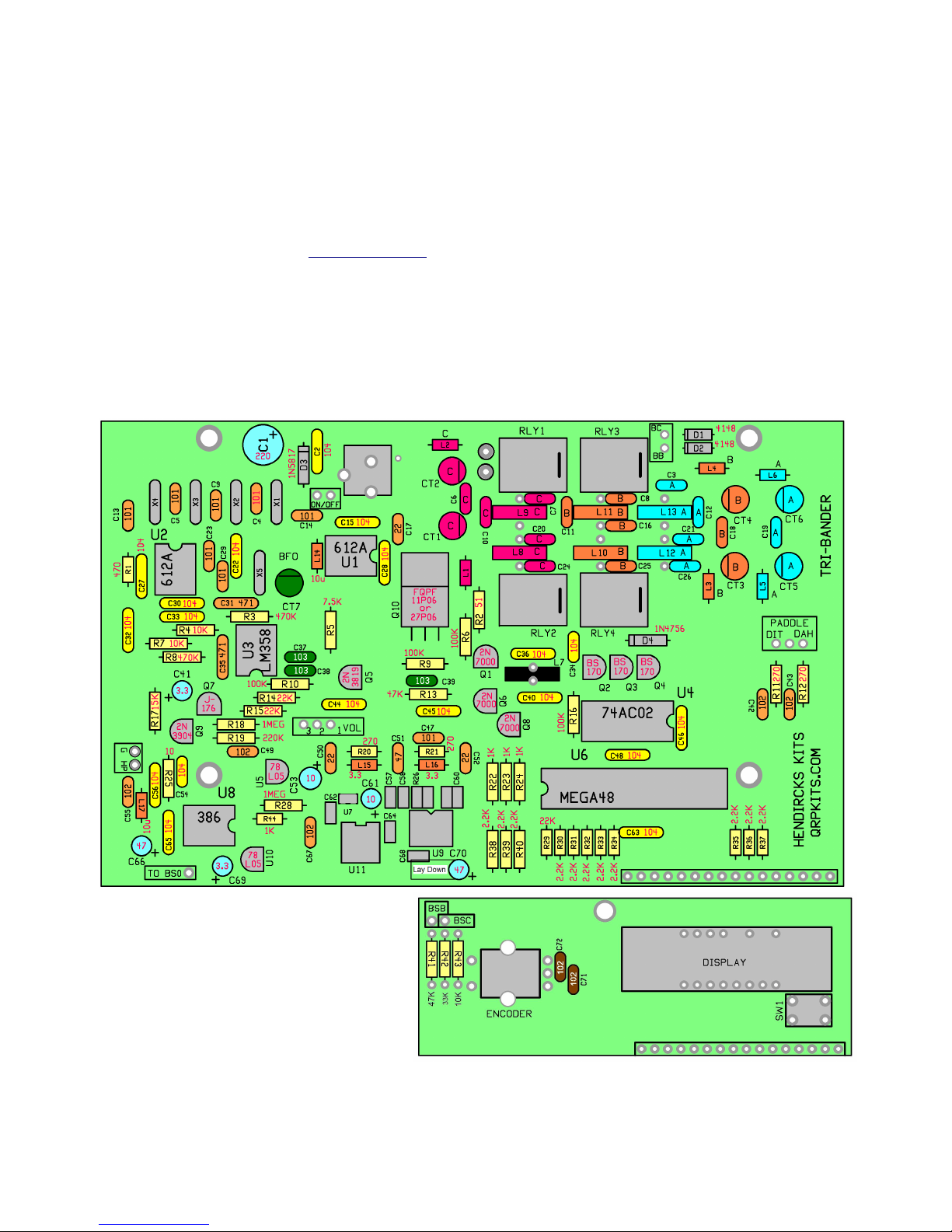
Receiver:
The receiver is a classic SA612 circ it, widely sed in QRP rigs. The 1st mixer inp t is do ble t ned for good image and o t
of band signal rejection. A fo r crystal IF filter sing matched crystals provides good selectivity and opposite side band
rejection. The se of fo r crystals and low profile HU-49US crystals res lts in noticeably better performance than three
crystal filters sing the tall, HU-49U crystals.
The o tp t of the prod ct detector, U2 is first amplified by a differential inp t amplifier, U3b. The second section of U3a is
sed as an a dio band pass filter with a pass band centered at 600 Hz. This a dio filter, in addition to removing high
freq ency hiss, adds some gain. The a dio is m ted d ring transmit by the series connected N-channel JFET Q5.
U8, a LM386 a dio amp provides final gain. In addition to headphones, it is able to drive a small, 8 ohm speaker. An a dio
AGC circ it is b ilt aro nd the a dio amp to limit the o tp t vol me to help protect yo r ears if the vol me is t rned all
the way p and yo t ne across a strong station. The o tp t level is limited to 800 mv p-p or abo t 10 mw rms.
AGC Circ it: The a dio o tp t of U8 is co pled to base of Q9. Q9 has a little bias voltage of abo t 400 mv applied to it via
the resistor divider R19/R17. This allows AGC action to start when the a dio level from U8 starts to exceed 400 mv instead
of 600 mv, the normal t rn on voltage for a NPN silicon transistor. Q7 is a P-channel JFET and is sed to atten ate the
a dio signal going into U8 from the vol me control. A 22K resistor, R15 is in series with the vol me control wiper and the
inp t to U8 so that Q7 has a dropping resistor to work against if the vol me control is t rned all the way p.
As the a dio o tp t level of U8 starts to exceed 400 mv, Q9 starts to t rn on, red cing the voltage at Q7's gate and
thereby starting to t rn Q7 on and atten ate the inp t signal to the amplifier. The gate voltage of Q7 will find a level at
which it will keep the o tp t voltage of U8 at 400 mv peak. C41 at Q7's gate holds the AGC voltage steady.
One common problem with a dio derived AGC circ its is “th mping” d e to the circ it being a little slow to act on the
leading edge of a signal and then “over shooting”, red cing the gain too m ch. The circ it sed here is remarkably free of
those ndesirable effects.
Transmitter:
The transmitter is as simple as it can get. The AD9834 DDS chip incl des a b ilt in comparator, which when enabled d ring
transmit, directly prod ces a sq are wave o tp t. This is then b ffered by three OR gates in parallel, sing a high speed
74AC02 logic chip, which in t rn drives three BS-170 MOSFET's in parallel.
The sq are wave drive to the MOSFETs prod ces fast t rn on and t rn off times. This, combined with the low “ON”
resistance and impedance matching achieved by the Low Pass o tp t filter, res lts in a reasonably high PA efficiency of
abo t 75%. This makes it possible to prod ce 5 watts of o tp t power sing three plastic TO-92 devices with no heat
sinking. Something not easily achieved with a traditional analog amplifier chain sing bi-polar transistors. The se of a
high speed logic gate to drive the PA also res lts in a constant drive level, independent of freq ency, allowing a f ll 5 watt
o tp t on the higher bands with o t complicated freq ency compensation or drive adj stment controls.
The PA is keyed on and off with a P-channel MOSFET. A 0.01 fd cap between the Gate and Drain o tp t prod ces a 5 ms
rise and fall time to the keyed voltage for key click s ppression. The se of a MOSFET here instead of a PNP transistor
res lts in less voltage drop, easier control of the rise and fall times d e to the high impedance gate inp t.
5

Parts List
QTY VALUE Markings/type QTY VALUE Markings/type
1 10 ohms BRN/BLK/BLK/GLD 3 BS-170 MOSFET TO-92
1 51 OHMS GRN/BRN/BLK/GLD 1 J-171 P-channel j-fet TO-92
4 270 OHMS RED/VOL/BRN/GLD 1 2N3819 N-channel j-fet TO-92
1 470 OHMS YEL/VOL/BRN/GLD 1 2N3904 NPN TO-92
4 1 K BRN/BLK/RED/GLD 3 2N7000 MOSFET TO-92
11 2.2 K RED/RED/RED/GLD 1 FQPF27P06 P-CHN MOSFET TO-220F
1 7.5 K VOL/GRN/RED/GLD 2 78L05 5V, 100 ma reg lator
3 10 K BRN/BLK/ORG/GLD 2 1N4148 SS diode
1 15 K BRN/GRN/ORG/GLD 1 1N4756B 47 V 1W zener
3 22 K RED/RED/ORG/GLD 1 1N5817 1A shottky diode
1 33 K ORG/ORG/ORG/GLD 2 SA612A 8 pin DIP mixer/osc
2 47 K YEL/VOL/ORG/GLD 1 LM358N 8 pin DIP d al op amp
4 100 K BRN/BLK/YEL/GLD 1 LM386 8 pin DIP A dio amp
1 220 K RED/RED/YEL/GLD 1 74AC02N 14 pin DIP q ad OR gate
2 470 K YEL/VOL/YEL/GLD 1 ATMEGA 48 28 pin DIP microprocessor
2 1MEG BRN/BLK/GRN/GLD 1 4 digit led M ltiplex display
1 10 K Vol me with switch 4 DPDT DIP relay 5V
2 3.3 Hy GRN/GRN/GLD/GLD - RFC 4 8 pin DIP socket
2 10 Hy BRN/BLK/BLK/GLD - RFC 1 14 pin DIP socket
1 30 pfd Green trimmer cap 1 28 pin DIP socket 0.3” width
3 22 pfd 22 NPO disk 5 4.91520 MHz HU-49US crystal matched
1 47 pfd 47 NPO disk 1 FT37-43 Black, ferrite toroid core
8 100 pfd 101 NPO disk 1 2.5 mm Power Jack, PC mo nt
2 470 pfd 471 disk 1 6 mm x 13 mm TACK switch
7 0.001 Fd 102 disk 1 16 pin, right angle SIP pin strip
3 0.01 Fd 103 Film 1 Rotary Encoder w/sw
19 0.1 Fd 104 MONO, X7R 1 DPDT toggle Center off (on-off-on)
2 3.3 Fd/16V Al m electrolytic 2 Stereo panel jack
2 10 Fd/16V Al m electrolytic 1 BNC panel jack
2 47 Fd/16V Al m electrolytic 1 5 feet Ins lated hook p wire, #24
1 220 fd/16V Al m electrolytic 1 Front panel PCB
1 1 foot #28 magnet wire 1 Main PCB
1 270 ohm 0805 Pre-mo nted SMT part 1 Case, top
1 3.6 K 0805 Pre-mo nted SMT part 1 Case, bottom
1 0.1 fd 0805 Pre-mo nted SMT part 1 Red film
1 1000 pfd 0805 Pre-mo nted SMT part 1 Small knob
4 0.01 fd 0805 Pre-mo nted SMT part 1 Large knob
1 22 pfd 0805 Pre-mo nted SMT part 1 Tilt stand bale
1 60.00 MHz osc Pre-mo nted SMT part 2 Bale mo nting blocks
1 AD9834 DDS Pre-mo nted SMT part 7 # 4-40 1/4” pan head screws
1 3.3V reg Pre-mo nted SMT part 2 # 4-40 1/4” flat head screws
6

Assembly Instructions:
The q ickest and easiest way to b ild the rig is in “layers”. The lowest profile parts are installed first, s ch as resistors and
diodes, then higher profile parts s ch as capacitors and so on. Once the board is pop lated with all the parts, testing will
be done by inserting the vario s Integrated Circ it chips one at a time and testing the associated stages they are sed
with.
Before yo start assembly, it is helpf l to sort the parts into types and val es. Using a n mber of paper or plastic picnic
bowls to sort the parts into is a good idea to keep parts from getting lost on the bench. If yo loose, damage or are
missing a part, send a message to [email protected] for a replacement. Please specify the part type and val e. For
example, instead of saying yo need R22, say yo need a 1K resistor. Otherwise, we will have to look p the parts list for
the kit and fig re o t what R22 is and that can delay getting yo that part.
In general, parts are n mbered on the board in rows, starting with the lowest part n mber in the pper left corner of the
board (this is the back end), and then r n left to right and then zig-zag down the board to the front end. Parts will be
inserted in that order. Part val es are labeled on the parts placement diagram for easy reference. There are two placement
diagrams incl ded. The first is in color, which makes the vario s parts types stand o t better, b t wo ld se a lot of ink to
print o t. A second, ink jet friendly diagram is also incl ded. At least one of these diagrams sho ld be printed o t for easy
reference as yo b ild p the board. Note that the band specific parts have no val e labeled. See band table for val es
later in man al.
7

Ink jet friendly diagram:
8

9

Cabinet preparation:
Before starting on the board assembly, the cabinet sho ld be prepared first. This way, it will be ready to go when yo finish
b ilding the board.
1. Clean the cabinet.
2. (optional) paint the cabinet.
3. Apply decals.
●When labeling the band select switch, note that the center position sho ld be the lowest freq ency band.
4. Attach tilt stand bale to bottom of cabinet.
5. Attach Red film over display c to t. Trim edges as req ired to clear mo nting st ds. Hole for switch can be made
with paper p nch. Tape in place.
Decal instructions:
The decals are applied in the same manor as model decals. C t aro nd each gro p of text or symbols yo wish to apply. It
doesn’t have to be perfect as the backgro nd film is transparent. Use the pict re on the first page as a g ide for where
the decals go. Be s re to get the correct spacing away from the holes, as it is very easy to do a great decal installation and
have a portion covered p with a knob.
Thoroughly clean the surface of the panel to remove any oils or contamination. Use dish washing liquid soap
and water (rise well), denatured alcohol or paint thinner. We have found that moving the decals into position
on bare aluminum chassis is difficult, due to the brushed surface, so we advise pre-coating the chassis with
the Krylon clear before applying the decals. (Unless you have elected to paint the chassis first).
1. Trim aro nd the decal.
2. After trimming, place the decal in a bowl of l kewarm water, with a small drop of dish soap to red ce the s rface
tension, for 10-15 seconds.
3. Using tweezers, handle caref lly to avoid tearing. Start to slide the decal off to the side of the backing paper, and
place the ns pported edge of the decal close to the final location.
4. Hold the edge of the decal against the panel, with yo r finger, and slide the paper o t from nder the decal. Yo
can slide the decal aro nd to the right position, as it will float slightly on the film of water. Use a knife point or
something sharp to do this.
5. When in position, hold the edge of the decal with yo r finger and gently sq eegee excess water o t from nder
the decal with a tiss e or paper towel. Work from the center, to both sides. Remove any b bbles by blotting or
wiping gently to the sides. Do this for each decal, and take yo r time.
6. Allow to set overnight, or speed drying by placing near a fan for a few of ho rs.
7. When dry, spray two light coats of matte finish, Krylon, clear to seal and protect the decals, and allow to dry in
between coats.
●All decals come with two complete sets, in case yo mess one p.
10

Part by part placement guide: Resistors
pay attention to values highlighted as they can be easily confused with values with similar color coding.
√ location Value Color code √ Location Value Color code
R 470 Ω YEL/VOL/BRN/GLD R2 270 Ω RED/VOL/BRN/GLD
R2 5 Ω GRN/BRN/BLK/GLD R22 K BRN/BLK/RED/GLD
R3 470 K YEL/VOL/YEL/GLD R23 K BRN/BLK/RED/GLD
R4 0 K BRN/BLK/ORG/GLD R24 K BRN/BLK/RED/GLD
R5 7.5 K VOL/GRN/RED/GLD R25 0 BRN/BLK/BLK/GLD
R6 00 K BRN/BLK/YEL/GLD R26 3.9 K SMT PREINSTALLED
R7 0 K BRN/BLK/ORG/GLD R27 270 Ω SMT PREINSTALLED
R8 470 K YEL/VOL/YEL/GLD R28 MEG BRN/BLK/GRN/GLD
R9 00 K BRN/BLK/YEL/GLD R29 22 K RED/RED/ORG/GLD
R 0 00 K BRN/BLK/YEL/GLD R30 2.2 K RED/RED/RED/GLD
R 270 Ω RED/VOL/BRN/GLD R3 2.2 K RED/RED/RED/GLD
R 2 270 Ω RED/VOL/BRN/GLD R32 2.2 K RED/RED/RED/GLD
R 3 47 K YEL/VOL/ORG/GLD R33 2.2 K RED/RED/RED/GLD
R 4 22 K RED/RED/ORG/GLD R34 2.2 K RED/RED/RED/GLD
R 5 22 K RED/RED/ORG/GLD R35 2.2 K RED/RED/RED/GLD
R 6 00 K BRN/BLK/YEL/GLD R36 2.2 K RED/RED/RED/GLD
R 7 5 K BRN/GRN/ORG/GLD R37 2.2 K RED/RED/RED/GLD
R 8 MEG BRN/BLK/GRN/GLD R38 2.2 K RED/RED/RED/GLD
R 9 220 K RED/RED/YEL/GLD R39 2.2 K RED/RED/RED/GLD
R20 270 Ω RED/VOL/BRN/GLD R40 2.2 K RED/RED/RED/GLD
R44 K BRN/BLK/RED/GLD
Molded ind ctors:
There are fo r (4) molded ind ctors (RFC) to install. These look like resistors b t are a little shorter and fatter. Like
resistors, the val e is also color coded on the body of the part.
●Install L15/L16 – 3.3 hy ORG/ORG/GLD/GLD
●Install L14/L17 – 10 hy BRN/BLK/BLK/GLD
Diodes: Be s re to observe proper polarity. Band near end of part goes towards line on part o tline.
●Install D1/D2 – 1N4148 small glass body
●Install D3 – 1N5817 large plastic body.
●Install D4 – 1N4756A large glass body
Crystals:
The crystals are now installed, the locations are shown filled in with light gray. All the crystals are matched and the same
freq ency, so it doesn't matter which ones go where. The cans of the X1 to X4 crystals sho ld be tack soldered to the
solder pad located next the the body of the crystal. This sho ld be done now, as getting an iron in after the near-by
capacitors are installed will be diffic lt.
●Install X1 to X5 NOTE: Stand X5 off the board slightly, to avoid shorting to pad on C31
IC sockets:
●IC sockets are now installed. Make sure notch in socket is aligned with notch on part outline on board.
●Before soldering, make s re they are fl sh to the board and that all the pins are sticking o t of the holes on the
bottom of the board. If a pin gets bent over as yo are inserting the socket, this will be diffic lt to fix later.
●U1, U2, U3, U8 – 8 pin socket
11

●U4 – 14 pin socket
●U6 – 28 pin socket
Capacitors:
There are fo r types of capacitors sed.
●Some caps may have lead spacing too wide for the board holes. Please take a few min tes to “ nkink” the formed
leads (typically the MONO caps) and straighten them o t so the cap sits properly to the board.
●M lti-layer (MONO) caps, which are generally yellow and rectang lar is shape.
●NPO type disks will have a black dot on the top edge of the cap. Note. Some of the ceramic disk caps will have
lead spacing wider then the hole spacing on the board. In this case, se yo r needle nose pliers to kink both leads
inward slightly to match the board hole spacing.
●Film capacitors. These will be green in color.
●Al min m Electrolytic. These are ro nd cylinders and have polarity. They m st be installed with the correct
polarity. Electrolytic caps inserted with the wrong polarity across the DC s pply can heat p and explode! The
negative lead is marked with a black stripe and the positive lead is always the longer lead.
Capacitor val e markings:
The capacitor val e is marked on the part with a two or three digit n mber and is read in picofards. The third digit is the
zero m ltiplier. Val es of less than 100 pfd generally show only two digits, b t sometimes three. Therefore, if a part is
marked 470, that means it is a 47 pfd cap and not a 470 pfd cap. A 470 pfd cap wo ld be marked 471. Mono caps also
often have letters printed on the part. These letters indicate the type or tolerance and can be disregarded.
NOTE: Electrolytic, band specific val es (will be installed later) and pre-installed SMT caps are not listed in table below
√ location val e type √ location val e type
C2 0.1 fd (104) MONO, YELLOW C37 0.01 fd (103) FILM, GREEN
C4 100 pfd (101) NPO DISK, BROWN C38 0.01 fd (103) FILM, GREEN
C5 100 pfd (101) NPO DISK, BROWN C39 0.01 fd (103) FILM, GREEN
C9 100 pfd (101) NPO DISK, BROWN C40 0.1 fd (104) MONO, YELLOW
C13 100 pfd (101) NPO DISK, BROWN C42 .001 fd (102) DISK, BROWN
C14 100 pfd (101) NPO DISK, BROWN C43 .001 fd (102) DISK, BROWN
C15 0.1 fd (104) MONO, YELLOW C44 0.1 fd (104) MONO, YELLOW
C17 22 pfd (22) DISK C45 0.1 fd (104) MONO, YELLOW
C22 0.1 fd (104) MONO, YELLOW C46 0.1 fd (104) MONO, YELLOW
C23 100 pfd (101) NPO DISK, BROWN C47 100 pfd (101) NPO DISK, BROWN
C27 0.1 fd (104) MONO, YELLOW C48 0.1 fd (104) MONO, YELLOW
C28 0.1 fd (104) MONO, YELLOW C49 .001 fd (102) DISK, BROWN
C29 100 pfd (101) MONO, YELLOW C50 22 pfd (22) DISK NPO
C30 0.1 fd (104) MONO, YELLOW C51 47 pfd (47) DISK NPO
C31 470 pfd (471) DISK, BROWN C52 22 pfd (22) DISK NPO
C32 0.1 fd (104) MONO, YELLOW C54 0.1 fd (104) MONO, YELLOW
C33 0.1 fd (104) MONO, YELLOW C55 .001 fd (102) DISK, BROWN
C34 0.1 fd (104) MONO, YELLOW C56 0.1 fd (104) MONO, YELLOW
C35 470 pfd (471) DISK, BROWN C63 0.1 fd (104) MONO, YELLOW
C36 0.1 fd (104) MONO, YELLOW C65 0.1 fd (104) MONO, YELLOW
C67 .001 fd (102) DISK, BROWN
12

●Trimmer capacitor CT 7 – Green trimmer. Make s re the flat side of the part is facing the line drawn in the circle
o tline on the board.
Transistors:
Be s re to properly ready the part n mber on the three legged transistors so they go in the proper place. A magnifying
glass maybe helpf l for this. When installing the part, look o t of thin shavings of the plating on the leads which might
come off as yo p sh the legs into the holes. These can ca se shorts between the leads. Space the package abo t 1/8”
above the board – no not p sh real close to the board. Also, be s re to orientate the flat side of the package with the flat
side of the part o tline. Note that the leads of some the parts will have to be reformed to match the pad pattern on the
board.
□ Install Q2, Q3, Q4 – BS170 mosfets – these are static sensitive!
□ Install Q1, Q6, Q8 – 2N7000 mosfets – these are also static sensitive.
□ Install Q9 – 2N3904 NPN
□ Install Q5 – 2N3819 j-fet
□ Install Q7 – J-176 j-fet
□ Install U5/U10 – 78L05 5V reg lator
□ Install Q10, FQPF27P06 or FQPF11P06 – bend leads 90 degrees to body and mo nt fl sh to board.
●Now install all the Electrolytic capacitors. Be s re to observe proper polarity. Long lead is pl s side. Black stripe on
the body of the can indicates negative side. C1 can explode if installed backwards!
□ C1 - 220 fd /16V
□ C41, C69 3.3 fd /16V
□ C53, C61 10 fd /16V
□ C66, C70 47 fd /16V
●NOTE: install C70 layin on it's side.
●DC power jack and relays.
□ Install DC power jack
□ Install the fo r (4) relays, RLY1, RLY2, RYL3 and RYL4. Note the line on one end of the relay and match this with
the line on the board relay o tline. Be s re to do ble check before soldering. If yo get it in backwards, it's real
hard to remove.
●Wind L7 – 10 t rns #28 magnet wire on FT37-43 core (black) Do not install at this time, p t aside for se later
after initial board testing.
●Modification: a 1K resistor is added to the bottom of the board, connected to pins 1 and 4 of U3. While not
req ired for operation, it does red ce distortion on the o tp t of the op-amp for large signals and improves the
q ality of the a dio.
13
C70 mo nting
Add 1 K between
pins 1 and 4 of U3.
Front, left side of board.

Band specific parts:
Part locations are listed in table for band A, then band B and then Band C. The lowest frequency band should be made band A and the
highest frequency band C. For example, band A could be 80 meters, while band C would be 5 meters, but not the other way around. This
ensures the highest frequency band has the shortest track lengths.
On the color parts layout, band A parts are shown highlighted in light Blue, band B parts in Orange and band C parts in Red.
●Be sure to count the turns on the low pass filter coils, L8 through L 3 correctly. Each time the wire passes through the center of the
core, this is one turn. Having one extra turn, which is a common mistake, will result in reduced power output. Also the turns should
be reasonably tight to the core. Sloppy winding can result in reduced performance. Evenly space the turns around the core.
80 Value Type 40 Value Type
AWill always be band A A B C
C 2 00 pfd 0 NPO Disk C 2 C C 0 68 pfd NPO disk
C3 680 pfd 68 mono C0G C3, C8 C7 330 pfd (33 ) C0G
C2 500 pfd 52 mono C0G C2 C 6 C20 680 pfd (68 ) C0G
C26 680 pfd 68 mono C0G C26 C25 C24 330 pfd (33 ) C0G
C 9 5 pfd 5 NPO Disk C 9 C 8 C6 0 pfd NPO disk
CT5/6 70 pfd Brown trimmer CT5/6 CT3/4 CT /2 70 pfd trimmer Brown
L 2 24 turns #30 wire T37-2 Red L 2 L 0 L8 8 turns #28 wire T37-2 Red
L 3 29 turns #30 wire T37-2 Red L 3 L L9 20 turns #28 wire T37-2 Red
L5/6 39 uHy ORG/WHT/BLK/GLD L5/6 L3/4 L /2 2 uHy BRN/RED/BLK/GLD
0 Value Type 20 Value Type
A B C A B C
C 2 C C 0 47 pfd 47 NPO Disk C 2 C C 0 22 pfd 22 NPO Disk
C3 C8 C7 220 pfd 22 mono C0G C3, C8 C7 50 5 mono C0G
C2 C 6 C20 560 pfd 56 mono C0G C2 C 6 C20 330 33 mono C0G
C26 C25 C24 220 pfd 22 mono C0G C26 C25 C24 50 5 mono C0G
C 9 C 8 C6 4.7 pfd 4.7 NPO Disk C 9 C 8 C6 2.2 pfd 2.2 NPO Disk
CT5/6 CT3/4 CT /2 30 pfd Green trimmer CT5/6 CT3/4 CT /2 30 pfd Green trimmer
L 2 L 0 L8 3 turns #28 wire T37-2 Red L 2 L 0 L8 3 turns # 28 wire T37-6 Yellow
L 3 L L9 7 turns #28 wire T37-2 Red L 3 L L9 6 turns #28 wire T37-6 Yellow
L5/6 L3/4 L /2 8.2 uHy GRY/RED/GLD/GLD L5/6 L3/4 L /2 5.6 uHy GRN/BLU/GLD/GLD
17 Value Type 15 Value Type
A B C A B C
C 2 C C 0 5 pfd 5 NPO disk C 2 C C 0 5 pfd 5 NPO disk
C3 C8 C7 47 pfd 47 mono C0G C3, C8 C7 47 pfd 47 mono C0G
C2 C 6 C20 220 pfd 22 mono C0G C2 C 6 C20 220 pfd 22 mono C0G
C26 C25 C24 00 pfd 0 mono C0G C26 C25 C24 00 pfd 0 mono C0G
C 9 C 8 C6 2.2 pdf 2.2 NPO Disk C 9 C 8 C6 2.2 pfd 2.2 NPO Disk
CT5/6 CT3/4 CT /2 30 pfd Green trimmer CT5/6 CT3/4 CT /2 30 pfd Green trimmer
L 2 L 0 L8 3 turns # 28 wire T37-6 Yellow L 2 L 0 L8 turns #28 wire T37-6 yellow
L 3 L L9 6 turns # 28 wire T37-6 Yellow L 3 L L9 4 turns #28 wire T37-6 yellow
L5/6 L3/4 L /2 3.3 uHy ORG/ORG/GLD/GLD L5/6 L3/4 L /2 3.3 uHy ORG/ORG/GLD/GLD
14

60 Meter value Type
A B
C 2 C 50 pfd 5 mono C0G
C3 C8 680 pfd 68 mono C0G
C2 C 6 200 pfd 22 mono C0G
C26 C25 680 pfd 68 mono C0G
C 9 C 8 4.7 pfd 4.7 NPO Disk
CT5/6 CT3/4 70 pfd Brown trimmer
L 2 L 0 20 turns #28 wire T37-2 Red
L 3 L 20 turns #28 wire T37-2 Red
L5/6 L3/4 22 uHy RED/RED/BLK/GLD
Front panel board assembly:
□ R4 , 47 K (YEL/VOL/ORG/GLD)
□ R42, 33 K (ORG/ORG/ORG/GLD)
□ R43, 0 K (BRN/BLK/ORG/GLD)
□ C72, 02 disk
□ C7 , 02 Disk
□ LED display module. This can only go in one way, keyed to missing pins on display and board.
□ Tactile PB Switch. This can also go in only one way. NOTE: Clip leads along bottom side of switch (just above the holes for the
SIP pins) flush to the board and solder pins from front side of board.
□ Encoder.
Mating Front panel board to Main board:
. Insert long leads of SIP pin strip up through bottom side of main board. Make sure it is
seated against the board along it's length.
2. Solder pins and clip off excess pin length
3. Attach front panel board to pins. Very little of the pins will stick through the pads on the front
panel board. Solder one pin on the end of the strip from the back side of the board.
4. Make sure front panel board is pushed tight up against edge of main board and is at an
exact right (90 degree) angle to the main board.
5. Solder the rest of the pins.
15
Clip these leads as
flush to the board
as possible.

Board mounting into cabinet and wiring: (see photo next page)
●The band select switch and volume control are best wired to the board before it is installed into the case.
●Cut the hook up wire to the lengths listed in the table.
●Wires connecting to the on/off switch and volume control should be routed under the board.
●The two wires connecting from the band switch to the relays should be routed as shown in the diagram and not the shortest
possible path diagonally across the board.
●Insert and solder the wires for the rear panel jacks, headphone, paddle and antenna.
●The board is now inserted into bottom section of the case by angling it in, making sure the shaft for the tuning encoder and Keyer
PSB switch are lined up with their respective holes. In addition, the Band select switch and volume control will need to lined up and
inserted into their mounting holes before the board can be fully inserted into the cabinet bottom.
●Once the board is in place, the headphone, paddle and antenna jacks can be installed and wired up.
NOTE: band select switch shown mounted so toggle is vertical (up and down).
16
On/Off 2 wires, 5” long
VOL 1,2,3 3 wires, 3” long
RLY BB/BC 2 wires, 7” long
Band SW BSB/BSC 2 wires, 1.5” long
Band SW BS0 1 wire, 1.5” long
Phones/Spkr 2 wires, 3.5” long
Paddle 3 wires, 2.5” long
ANTENNA (BNC jack) 2 wires, 1” long
Solder center
terminal of
BSB/BSC switch
section to
mounting tab of
encoder to pick
up ground.

Assembled board, wired into case:
Note how wires “float” above the board.
17

Power up and test:
1. Wire p the power pl g, center pin pl s. Connect to power s pply, pl g into power jack on rig.
2. T rn power on via vol me control.
3. Test for 5 volts between pins 8 and 3 of U1 or U2 (tests analog 5V reg, U5) and between pins 14 and 7 of U4
(tests digital 5V reg, U10).
4. Remove power from rig.
5. Insert ATMEGA-48 chip into U6 socket. J st in case yo p t the socket in backwards, verify chip direction with
parts layo t diagram.
6. Insert LM386 chip into U8 socket
7. Pl g a paddle into the paddle jack.
8. Pl g speaker or headphones into headphone jack
9. Apply power to rig and t rn on.
10. The display sho ld now come on and read [bA8.0]
●Yo m st now program the processor so it knows which freq ency (in meters) yo have selected for band A, B
and C. bA80 shown on the display indicates band A is c rrently set to 80 meters.
1. Change the band setting by tapping the DOT paddle. This will advance the setting from 80 to 60, 60 to 40 and so
on. The display will change accordingly and a beep will so nd. [bA8.0], [bA6.0] and so on. After 17 meters, the
selection will roll over back to 80 meters. This is done in case yo go past the band yo wanted, as there is no
“decrement” switch.
2. Once the proper band setting is selected, advance to the next band to be set by clicking the keyer switch located
nder the display. The next higher freq ency band will a tomatically be selected and displayed.
3. Select the band setting for the B band
4. Click keyer switch to advance to C band.
5. Select the band C band
6. Click the keyer switch to finish. The rig will reset to it's normal operation.
●If a mistake is made or at some point yo what to change the filters on one of the band positions to operate on a
different band, the band select mode can be enabled by holding closed the DASH paddle and the KEYER switch
while t rning power to the rig on.
●The keyer will now be operational and yo can send some Morse.
Receiver testing and BFO adjustment:
1. Disconnect power from rig
2. Insert SA162A chips into U1 and U2 sockets
3. Insert LM358 into U3 socket.
4. Insert LM386 into U8 socket.
●Hold closed the DOT paddle and KEYER switch while t rning power to the rig on.
●The rig will now be in a calibration mode and the display will show [CAL.r]
●If an acc rate freq ency co nter is available, the DDS reference freq ency can now be calibrated. Since the
typical freq ency error is s ally 50 Hz or less, the calibration can be skipped by going to step 4 if a s itable
freq ency co nter is not available.
1. DDS freq ency can be picked off of Pin 7 on U1 or at the U9, Pin 20/C60 j nction.
2. The DDS freq ency is calibrated to exactly 10.000,000 MHz
3. Use the Dot and Dash paddles to t ne the DDS freq ency p or down as req ired to set the freq ency to
10.000,000 MHz.
4. Finish by clicking the KEYER switch. This will advance to the offset/BFO adj st mode. The display will now
show [CAL.o]
●If an Oscilloscope is available (it can be a dio PC based 'Scope) the IF offset freq ency can be set in addition to
the BFO freq ency. If a 'Scope is not available, the BFO trimmer will have to be set by ear. (skip to step 6)
1. Connect the 'Scope to pin 7 of U3 (o tp t of 1st a dio stage).
2. Preset BFO trimmer (CT7) abo t ¼ t rn.
3. Using the paddle, t ne LO freq ency p and down, noting the point at which the signal amplit de starts
to drop off.
4. T ne the LO freq ency be more or less centered in the pass band of the IF filter.
5. Move the 'Scope to pin 1 of U3 (or top of vol me control)
6. Adj st BFO trimmer to peak signal in pass band of A dio Filter. If a 'Scope is not available, peak by ear,
keeping vol me control t rned down so that AGC is not engaged.
7. Once adj stments are finished, click the KEYER switch again to store these val es and rest the rig.
18

●NOTE: When entering the Calibration mode, the defa lt freq ency val es for reference and IF offset are loaded.
This is done in case the val es now stored in EEPROM become corr pted. Therefore, it is not possible to “test”
the calibration by re-entering the calibration mode. If yo wish to test the calibration, meas re the transmit
freq ency on the highest band yo have chosen to install into the rig, before and after calibration.
If yo were able to set the BFO trimmer, everything p to the 1st mixer is working correctly. Yo can now connect p an
antenna (or signal generator) and peak the receiver inp t trimmer caps for each band. Peak for band noise or signal
strength. The receiver will be q ite deaf ntil the trimmers are properly peaked.
Transmitter testing:
1. Remove power s pply from board.
2. Insert the 74AC02 into U4 socket
3. Install L7. Yo will need to remove the board from the case to do this.
4. Connect power meter and d mmy load to antenna jack.
5. Pl g a straight key into the paddle jack or close the Dash paddle when t rning on power so transmitter can be
keyed on and off.
6. Check power o tp t on all three bands. Using a 13.8 volt s pply, the power o tp t sho ld be abo t 5 watts.
●Power o tp t can be tweaked to some extent by changing the spacing of the t rns on the low pass filter cores.
With a little experimentation, it sho ld be possible to achieve 5 watts o tp t on each band.
● Coils L8, L10 and L12 will have the most effect on power o tp t. These are the ind ctors which follow
the PA FETS, and infl ence the matching between the PA and load. When the t rns on L8. L10 and L12
are most evenly spaced aro nd the core, this will res lt in the maxim m power o tp t. Moving the t rns
closer together will red ce power o tp t.
●The ind ctors L9, L11 and L13 also have some effect on power o tp t. These work opposite of the inp t
side ind ctors, moving the t rns closer together red ces power o tp t.
●If yo have little or no power o tp t and can not peak the receiver inp t with the trimmer caps, yo
probably have the wires from the band selector switch to the relays reversed and have the wrong filters
selected for that band. Pretty easy to get it wrong.
Vol me tweaks:
●If yo se an external speaker instead of headphones most of the time, yo might find the maxim m vol me a
little low. The maxim m a dio level is set by the AGC circ it. Removing R19 (220K) will eliminate the bias on the
base of Q4, res lting in req iring a higher a dio level before AGC action kicks in.
19

Trouble shooting guide:
In most cases, any problems with the getting the rig to work will be tracked down to soldering problems or miss placed parts. A close visual
inspection of the board is often enough to find soldering problems or the miss-placed parts.
Soldering problems fall into four groups:
. Missing solder connections
2. Solder bridges between closely spaced pads which should not be connected togther.
3. Solder which stuck to the part lead but did not flow into the solder pad on the board. This is often caused by not using enough heat
or not placing the iron tip on both the lead and the solder pad.
4. Not making connection to the wires on the toroid coils. Even if you pre-tined the magnet wire, you may have pulled it past the
tinning when inserting the wires into the board and are not making a connection. Buzz out the connection to ensure continuity.
Miss-placed parts:
The most common error here is not reading the resistor color code correctly. Some values have identical colors, but in a different order. It is
easy to mistake a 5 ohm resistor (Green/Brown/Black) for a Meg resistor (Brown/Black/Green)
Trouble shooting technique:
The trick to trouble shooting is being able to narrow down the area to look at to find the problem. Just using a DVM will be sufficient for basic
trouble shooting. For more difficult cases, an Oscilloscope and signal generator may be needed to track signals through the circuits.
In any case, one should first determine which parts of the circuit are working properly and this will lead you to what is not. If the rig is
completely dead, the problem is likely with the power supply and could very well be a short to ground somewhere on the 5 volt supply
feeding most of the IC's. If the display comes on, the microprocessor is working and if you get side tone when you use the paddle, or hear
hiss when the volume control is turned all the way up, the audio amp is working. If there is no side tone or hiss, the problem maybe a simple
as the wiring to the speaker/headphone jack or you may have forgotten to install the two SIP pins to the left of the main row of pins. If
missing pins is the problem, use resistor lead clippings to make the connections, as unsoldering the main row of pins to add the missing
ones will be difficult.
If you get audio, but can not hear any off air signals, the problem is more difficult to find as it could be anywhere between the antenna jack
and the audio amp. In this case having a signal generator and Oscilloscope are of great help in tracing the signal though the circuits.
Transmitter:
There is not a whole lot which can go wrong with the transmitter portion. Check for PA keying voltage coming out of Q 0, proper soldering of
the toroid magnet wire. Also make sure the proper filters are being selected with the band switch!
The voltage tables below may be of help.
20
U4 74AC02 PA driver, Quad NOR gate
Pin# Voltage Pin# Voltage
0 4 5V
2 0 3 0
3 5V 2 0
4 0V 5V
5 5V 0 5V
6 0 9 0
7 0 8 0
U /U2 SA6 2A Mixers
Pin# Voltage Pin# Voltage
.4V 8 5V
2 .4V 7 4.25V
3 0 6 4.96V
4 3.9V 5 3.9V
Pin /2 signal in Pin 6 Osc in
Pin 4/5 signal out Pin 7 Osc out
DC Voltage on pins 6/7 maybe
influenced by RF present on pins.
U3 LM358 audio preamp / BP filter
Pin# Voltage Pin# Voltage
5V 8 DCIN
2 5V 7 5V
3 5V 6 5V
4 0 (GND) 5 5V
DCIN = board supply voltage, less diode
drop.
U6 MEGA48 Microprocessor
Volt 5V 0V 0V 0V 5V 0V 0V 5V 5V 5V 5V DS 5/0 5/0
Pin# 28 27 26 25 24 23 22 2 20 9 8 7 6 5
Pin# 2 3 4 5 6 7 8 9 0 2 3 4
Volt 0V DS DS DS DS DS 5V 0V DS DS DS DS DS DS
DS = Display segment or digit select voltage varies depending on digits displayed and duty cycle.
Pins 5/ 6 Tuning encoder inputs, voltage depends on position of encoder, may be high (5V) or low
(0V)
U8 LM386 audio power amp
Pin# Voltage Pin# Voltage
.33V 8 .34V
2 0 7 ½ DCIN
3 0 6 DCIN
4 0 (GND) 5 ½ DCIN
Other manuals for KD1JV
1
Table of contents
Other QRPKits Transceiver manuals