Sanyo CE28WN5-B User manual

Part No. SKSM0491 C3HAL/C3YAV MAY 2001
Colour Television
Service Manual
Model CE28WN5-B
CE32WN5-B
Service Ref. No. CE28WN5-B-00
CE32WN5-B-00
PRODUCT CODE: 111356800 (CE28WN5-B)
111356900 (CE32WN5-B)
ORIGINAL VERSION: Chassis No. EB6-A
Give complete "SERVICE REF. NO." for parts
order or servicing, it is shown on the rating sheet
on the cabinet back of the TV set.
Note
This TV receiver will not work properly in foreign
countries where the television transmission
system and power source differ from the design
specifications. Refer to the specifications for the
design specifications
CE28WN5-B
CE32WN5-B
Contents
Safety precautions/Specifications . . . . . . . . . . . . . . . . . . . . . . . . . . . . . . . . . . . . . . . . . . . . . . . . . . .2
Block diagrams . . . . . . . . . . . . . . . . . . . . . . . . . . . . . . . . . . . . . . . . . . . . . . . . . . . . . . . . . . . . . . .3~5
Cabinet Disassembly . . . . . . . . . . . . . . . . . . . . . . . . . . . . . . . . . . . . . . . . . . . . . . . . . . . . . . . . . . . .6
Adjustment and Repair Procedures . . . . . . . . . . . . . . . . . . . . . . . . . . . . . . . . . . . . . . . . . . . . . . .7~11
CPU Functions . . . . . . . . . . . . . . . . . . . . . . . . . . . . . . . . . . . . . . . . . . . . . . . . . . . . . . . . . . . . . . . . . . . . . . . . . . . . . .12~13
Component Locations . . . . . . . . . . . . . . . . . . . . . . . . . . . . . . . . . . . . . . . . . . . . . . . . . . . . . . . .14~15
IC Block Diagrams . . . . . . . . . . . . . . . . . . . . . . . . . . . . . . . . . . . . . . . . . . . . . . . . . . . . . . . . . .16~20
Pin description of semiconductors . . . . . . . . . . . . . . . . . . . . . . . . . . . . . . . . . . . . . . . . . . . . . . . . . .21
Part Description and reading of schematic diagram . . . . . . . . . . . . . . . . . . . . . . . . . . . . . . . . . . . . .22
Cabinet Parts List/TV Stand parts list . . . . . . . . . . . . . . . . . . . . . . . . . . . . . . . . . . . . . . . . . . . .23~24
Electric Parts List . . . . . . . . . . . . . . . . . . . . . . . . . . . . . . . . . . . . . . . . . . . . . . . . . . . . . . . . . . .25~34

-2-
C3HAL/C3YAV
SAFETY PRECAUTION
X-RADIATION PRECAUTION
The primary source of X-RADIATION in the television receiver is the picture tube. The picture tube is specially
constructed to limit X-RADIATION emissions. For continued X-RADIATION protection, the replacement tube
must be the same type as the original including suffix letter. Excessive high voltage may produce potentially
hazardous X-RADIATION. To avoid such hazards, the high voltage must be maintained within specified limit.
Refer to this service manual, high voltage adjustment for specific high voltage limit. If high voltage exceeds
specified limits, take necessary corrective action. Carefully follow the instructions for +B1 volt power supply
adjustment, and high voltage adjustment to maintain the high voltage within the specified limits.
PRODUCT SAFETY NOTICE
SPECIFICATIONS
Product safety should be considered when a component replacement is made in any area of a receiver.
Components indicated by mark in the parts list and the schematic diagram designate components in which
safety can be of special significance. It is particularly recommended that only parts designated on the parts list in
this manual be used for component replacement designated by mark . No deviations from resistance wattage
or voltage ratings may be made for replacement items designated by mark .
!
!
!
1: An isolation transformer should be connected in the
power line between the receiver and the AC line
when a service is performed on the primary of the
converter transformer of the set.
2: Comply with all caution and safety-related notes
provided on the cabinet back, inside the cabinet, on
the chassis or the picture tube.
3: When replacing a chassis in the cabinet, always be
certain that all the protective devices are installed
properly, such as, control knobs, adjustment covers
or shields, barriers, isolation resistor-capacitor networks
etc. Before returning any television to the customer,
the service technician must be sure that it is completely
safe to operate without danger of electrical shock.
COMMON SPECIFICATIONS
Power source AC 220~240V, 50Hz
Television system System I
Colour system PAL/NTSC4.43 (PAL/NTSC4.43/MTSC3.58 IN AV MODE)
Receiving channel UHF: #21~69
Aerial input impedance 75ohm
AV terminal
21 Pin SCART Terminal AV1:CENELEC standard with RGB
AV2:CENELEC standard with S-inputs
AV3:RCA Terminal, Video and Audio (L/R)
Sound output(Music) 12 x 2
DIFFERENCES CE28WN5-B CE32WN5-B
Dimensions (WxHxD) 779 x 524 x 511.5mm 880 x 577.5 x 567mm
Weight 32.5 Kg 46.3 Kg

-3- C3HAL/C3YAV
BLOCK DIAGRAM
This is a diagram for all models and therefore differs slightly from the actual block diagram.
IC801
<ST92R195>
CPU
IC803
MEMORY
SCL
SDA
IC802
ROM
IC201
<TB1251>
IF/VIDEO/
CHROMA/
DEF
Q242
Q243
Q244 CRT
R
G
B
Q121~Q133
TV-OUT
SIF-OUT
C-OUT
Y-OUT
13
8
15
18
AV1
AV2
TV-IN SC-1
SC-2
MONTO
-OUT
X132
X131
VIF
SIF
6
7
9
34
35
15
16
17
18
26
T451
FBT
V
H
D.Y
PCC
CONTROL
CS
CONTROL
Q432
Q431
H-OUT
EW-OUT
43
39
40
41
32
3
54
22
21
20
V-OUT IC501
3
6
C
Y
SYNC-IN
BLK
R
G
B
I2C BUS
BLK
B
G
R
CVBS-IN
61
60
47
46
45
44
25 26
24
23
43 1 - 15
80 - 63
T431
PROTECT-IN
PC-IN POWER
Q141
A101
TUNER
Aerial
Q762
Q782
Q782
FOCUS
SCREEN
Outline

-4-
C3HAL/C3YAV
IC1201
AV-SELECTOR
<MM1313>
1(V)
2(L)
4(R)
13(V)
14(L)
16(R)
7(V)
8(L)
9(Y)
10(R)
11(C)
41(V)
(V)34
31
8
15
18
8
5,6
10,11
13
29
33
32
37
38
MONITOR-OUT
Q1202
Q1203
Y-IN
C-IN
FRONT AV3
MONITOR-OUT
SC-1
(VIDEO/AUDIO-L/R)
SC-2
(VIDEO/Y/C/AUDIO-L/R)
SC-1
SC-2
K12J
K12M
FRONT-AV
K12H
L-OUT
R-OUT
IC3451
NICAM
&
STEREO
<TDA9875>
37
36
12
60
61
4
5
19
20
C-OUT
Y-OUT
SIF-IN
AUDIO L/R-OUT AUDIO-OUT
IC201
IF/VIDEO/
CHROMA
IC001
AUDIO-OUT
SDA/SCL
(VIDEO)
Y-OUT
C-OUT Q1205
Q1204/1207
I2C BUS
AV Selector
NICAM DECODER
IC801
CPU
25 31 28
24
23
43
61
60
36
46
45
44
1 - 7, 63 - 80
POWER
39
Relay SW
KEY-IN
37
SC1(AV1) 8-pin
SC2(AV2) 8-pin
RC-IN
BLK-OUT
B-OUT
G-OUT
R-OUT
Q806 CVBS
POWER-FAIL
DETECT
SCL
SDA
IC803
MEMORY
I2C BUS
CONTROL
IC802
ROM
System Control
Fig.-2
Fig.-3

-5- C3HAL/C3YAV
IC201
IF/VIDEO/
DEFLECTION
<TB1251>
26
41
32
V-Drive
H-Drive
Q431
IC501
V-Output<LA7846>
63
Q462
Deflection
Yoke
Horiz.
Coil
Vert.
Coil
T451
FlyBack Trans
CS SW
Screen Width Control
Pcc Control
Q461
D441
T431
Q431
Q451
H-Output
Drive Trans
L461/L462
EW-Out
Deflection Control

-6-
C3HAL/C3YAV
(A) (A)
CABINET DISASSEMBLY
CABINET BACK DISASSEMBLY
1. Remove 9 screws(A) for 28”
2. Pull out the cabinet back.
(A)
(A)
(A)
(A)
(A)
(A)
(A)
(B)
(A) (A)
(A)
(A)
(A)
(A)(A)
(A)
ANT.75Ω
FRONT
/DAVANTI
L/S
R/D
INT EXT/EST
REAR
/POSTERIORE
AV2 AV1
1. Remove 9 screws (A) + 2 screws (B) for
32”
2. Pull out cabinet back
(A)
(B)

-7- C3HAL/C3YAV
OPTION SETTING
[After replacing the Memory IC (IC803)]
The memory IC, IC803, stores the option data of TV set and service adjustments data for each circuit, therefore,
when the memory IC is replaced, it should be performed following setting and “SERVICE ADJUSTMENT” on next
page.
To enter to the Option Mode
+ Press and hold the F/OK button on the remote control and P▼button on the front panel of the TV. The option
window will appear on the screen.
To set the option mode
+ Highlight the desired option item by using the P▲or P▼ button .
+ To switch the option mode, use the Volume - (LEFT) or Volume + (RIGHT) button.
+ The data which is set in the option mode is stored into the memory IC automatically.
Following table shows the available option items and default setting mode.
Exit from the Service Mode
+ Press the RECALL button.
Option Mode Mode Description & Note
ON-TIMER ON or OFF On-timer available, default “ON”
SORT MODE AUTO TUNE/SORT Tuning mode, default “AUTO TUNE/SORT”
or AUTO TUNE
or ATS EURO PLUS
PLUG & PLAY ON or OFF Plug & Play mode, default “ON”
WELCOME TEXT ON or OFF Display message when first set up, default “ON”
CODE TEST OFF or ON For factory use, default “OFF”
WSS ON or OFF Wide Screen Signaling available, default “ON”
WIDE ON or OFF Wide mode, default “ON”
OPTION UK or IRELAND Destination option , default “UK”
312/313 Mode ON or OFF Teletext mode, default OFF
AV3 OPTION ON or OFF Front AV disable, default ON
3D SURROUND ON or OFF 3D Surround available, default ON
ON-TIMER ON
SORT MODE AUTOTUNE/SORT
PLUG & PLAY ON
WELCOMETEXT ON
CODETEST OFF
WSS ON
WIDE ON
OPTION UK
312/313 Mode OFF
AV3 OPTION ON
3D SURROUND ON
OPTION
ADJUST : EXIT : RECALL

-8-
C3HAL/C3YAV
SERVICE ADJUSTMENTS
[After replacing the Memory IC (IC803)]
The memory IC, IC803, stores the service adjustments data for each circuit, therefore, when the memory IC is
replaced, it should be performed “OPTION SETTING” on previous page and the following adjustments, refer to
further adjustment on page 14.
ADJUSTABLE SERVICE ADJUSTMENT
REGULAR
WIDE
To enter to the Service Mode
+ Press and hold the GREEN button on the remote control and then press the P▼button inside of the door. The
adjustment window will appear on the screen.
REGULAR
WIDE
OTHERS
TB1251
ADJUST
OK
SELECT:
EXIT : RECALL
IMPORTANT NOTICE
Do not attempt to adjust service adjustments not listed on the above otherwise it may cause
loss of performance and product safety.
Item No. OSD Description
1 P V-P Vertical Centre Adjustment
2 P H-P Horizontal Centre Adjustment
5 P V-S Vertical Size Adjustment
6 P H-S Horizontal Size Adjustment
7 P PCC Pcc Adjustment
8 P TRP Trapezoid Distortion Adjustment
10 P CNR Corner Adjustment
Item No. OSD Description
1 AGC AGC Adjustment
2 CUT Cut-Off Drive Adjustment
3 GRY G-Drive Adjustment
4 GRY B-Drive Adjustment
7 HBP H-Blanking Phase Adjustment
8 OSD OSD Positioning Adjustment
Note: Some items of the service adjustments for this chassis are controlled by the CPU, IC801, and the
adjustments are carried out by using the RC handset.

-9- C3HAL/C3YAV
To select the mode and service item and change data value
+ Highlight the desired adjustment mode by using the P▲or P▼button and then press the F/OK button.
+ To select the adjustment item, use the P▲or P▼button.
+ To change the service data, use the Volume -(LEFT) or Volume + (RIGHT) button.
+ The data which is set in the service mode is stored into the memory IC automatically.
Exit from the Service Mode
+ Press the RECALL button or turn off the TV set by using the Mains switch.
INITIALISATION OF MEMORY IC
To initialise the memory IC (IC803), press and hold the NORMAL button on te remote control and then press the P▲
button on the front panel of the TV set, and then turn the Mains switch Off and On. Now the initialisation is
completed.
When initialised the memory IC, all of the setting data (option data and service adjustment data) stored in the IC are
reset to the default value. So it is necessary to set the option settings and readjust the service adjustments listed on
left page.
REGULAR
1, AGC 38
Adjustment No.
and Item name Adjustment Data
WIDE
1. PV-P 1F
Adjustment No.
and Item name Adjustment Data
REGULAR mode WIDE mode

-10-
C3HAL/C3YAV
ADJUSTMENTS
IMPORTANT NOTICE
Do not attempt to adjust the following service adjustments except when adjustments are required in servicing
otherwise it may cause loss of performance and product safety.
1. Receive white raster pattern.
2. Set controls to normal.
3. Connect digital voltmetre to test point TP-B and GND.
4. Adjust voltage to 145 ±0.5V by using VR641.
1. Input and tune an RF signal which is UHF to the clear-
est station.
2. Connect digital voltmetre to test point TP-A and GND.
4. Enter to the service mode and select mode “REGU-
LAR”, and select item no.1 “REGULAR 1, AGC”.
5. Press the LEVEL+ or LEVEL - button to adjust volt-
age to be 3.2Vdc.
By using FOCUS VR, adjust focus control for well
defined scanning lines.
SCREEN ADJUSTMENT
1. Receive black & white pattern.
2. Enter to the service mode and select mode “REGU-
LAR”, and select item no. 2 “REGULAR 2, CUT”. The
horizontal line will appear on the screen.
3. Set the SCREEN VR for one colour to be just visible.
4. Using the numeric buttons shown set each colour to
minimum by decreasing to the point where any further
decrease resets the adjustment to maximum value.
BIAS ADJUSTMENT
5. By using the buttons 1, 2, 4, 5, 7, 8 on the remote
control, adjust the line to be white.
The key allocation is as follows;
Button No. Operation
1 Increase Red
2 Decrease Red
4 Increase Green
5 Decrease Green
7 Increase Blue
8 Decrease Blue
DRIVE ADJUSTMENT
6. Select item no.3 “REGULAR 3, GRY” (G-Drive) or 4
“REGULAR 4, GRY” (B-Drive) and adjust both initially
to 3F.
7. Change data value of each item by using LEVEL + or
LEVEL - button to obtain the proper white balance.
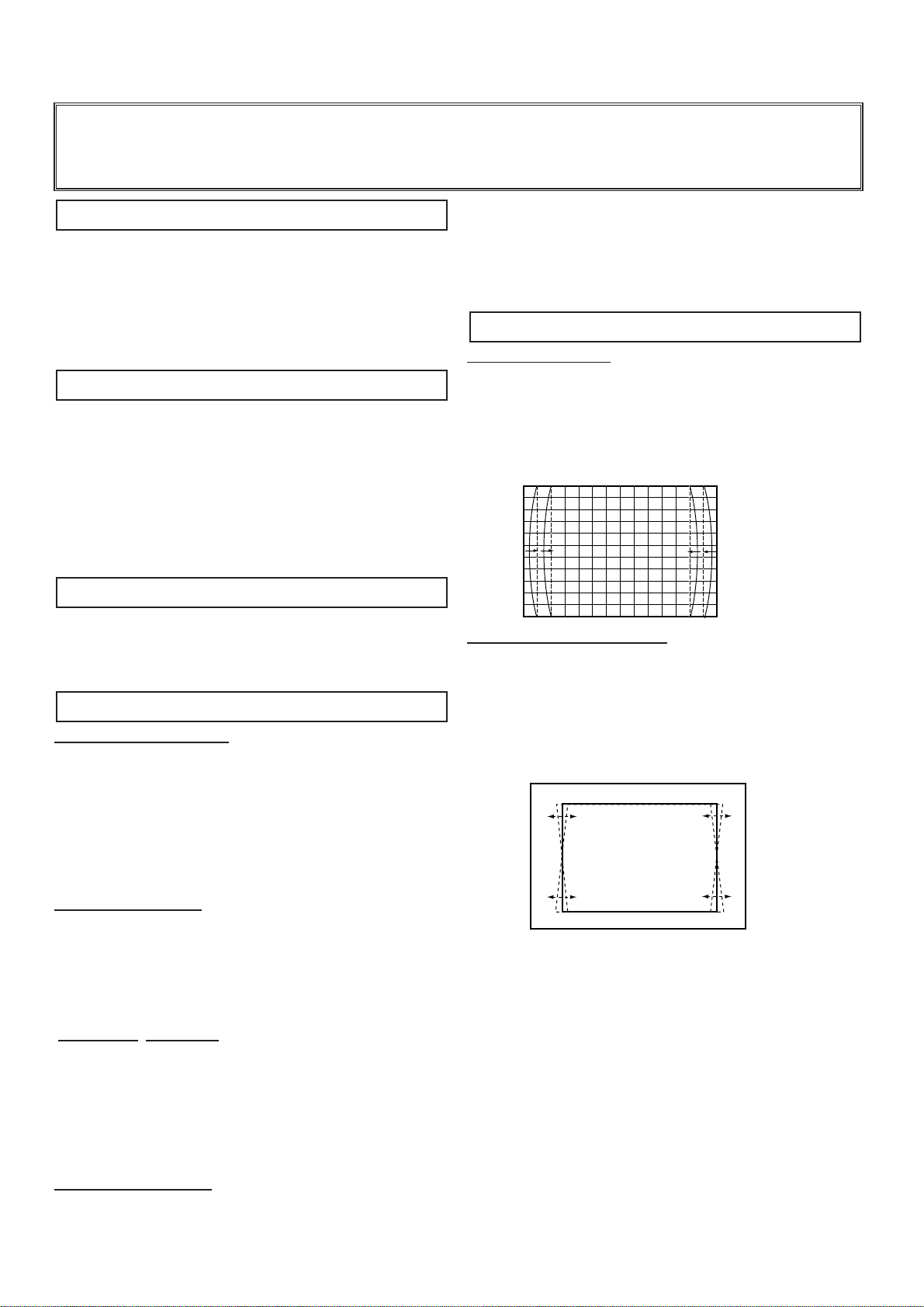
PCC ADJUSTMENT
1. Receive cross hatch pattern and set screen mode to
“FULL”.
2. Enter to the service mode and select mode “WIDE”,
and select item no. 7 “WIDE 7.P PCC”.
3. Press the LEVEL+ or LEVEL - button to adjust the
vertical line to be straight.
TRAPEZOID ADJUSTMENT
1. Receive cross hatch pattern and set screen mode to
“FULL”.
2. Enter to the service mode and select mode “WIDE”,
and select item no. 8 “WIDE 8.P TRP”.
3. Press the LEVEL+ or LEVEL - button to correct the
trapezum distortion of the vertical line.
PCC ADJUSTMENT
GREY SCALE ADJUSTMENT
FOCUS ADJUSTMENT
AGC ADJUSTMENT
+ B VOLTAGE ADJUSTMENT

-11- C3HAL/C3YAV
CORNER ADJUSTMENT
1. Receive cross hatch pattern and set screen mode to
“FULL”.
2. Enter to the service mode and select mode “WIDE”,
and select item no. 10 “WIDE 10.P CNR”.
3. Press the LEVEL+ or LEVEL - button to correct the
distortion of the vertical line around the corners.
HORIZONTAL CENTRING ADJUSTMENT
1. Receive circular pattern and set screen mode to
“FULL”.
2. Enter to the service mode and select mode “WIDE”,
and select item no. 2 “WIDE 2.P H-P”.
3. Press the LEVEL+ or LEVEL - button to adjust the
horizontal centre.
HORIZONTAL WIDTH ADJUSTMENT
1. Receive circular pattern and set screen mode to
“FULL”.
2. Enter to the service mode and select mode “WIDE”,
and select item 6 “WIDE 6.P H-W”.
3. Press the LEVEL+ or LEVEL - button to adjust the
horizontal width.
1. Receive circular pattern and set screen mode to
“FULL”.
2. Set controls to normal.
3. Connect high-voltage meter to the anode of CRT and
GND.
4. Confirm that voltage is 29.5±1.0kV for 28” model.
30.5±1.0kV for 32” model.
VERTICAL CENTRING ADJUSTMENT
1. Receive circular pattern and set screen mode to
“FULL”.
2. Enter to the service mode and select mode “WIDE”,
and select item no. 1 “WIDE 1.P V-P”.
.3 Press the LEVEL+ or LEVEL - button to adjust the
vertical centre.
VERTICAL HEIGHT ADJUSTMENT
1. Receive circular pattern and set screen mode to
“FULL”.
2. Enter to the service mode and select mode “WIDE”,
and select item no. 5 “WIDE 5.P V-S.
3. Press the LEVEL+ or LEVEL - button to adjust the
vertical height.
1. Receive circular pattern .
2. Enter to the service mode and select mode “REGU-
LAR”, and select item no. 7 “REGULAR 7.HBF”.
3. Press the LEVEL+ or LEVEL - button to adjust the
centre of picture image to be screen centre.
1. Receive circular pattern and set screen mode to
“FULL”.
2. Enter to the service mode and select mode “REGU-
LAR”, and select item no. 8 “REGULAR 8 OSD”. The
OSD test bar will appear on the top of screen.
3. Press the LEVEL+ or LEVEL - button to adjust prop-
er OSD positioning.
❚❚❚❚❚❚❚❚❚❚❚❚❚❚❚❚❚❚❚❚
OSD POSITIONING ADJUSTMENT
H-BLANK ADJUSTMENT
VERTICAL ADJUSTMENT
HIGH-VOLTAGE CONFIRMATION
HORIZONTAL ADJUSTMENT

-12-
C3HAL/C3YAV
CPU PORT FUNCTIONS
Pin No. Function Name Function IN/OUT
1 MMU0 External memory 0 OUT
2 MMU3 External memory 3 OUT
3 ADDR10 Address bus 10 OUT
4 DSN Data Strobe
5 ADDR11 Address bus 11 OUT
6 ADDR9 Address bus 9 OUT
7 ADDR8 Address bus 8 OUT
8 RWN Read Write Strobe
9 GND
10 VDD Power Supply IN
11 OSC-IN Clock Input IN
12 OSC-OUT Clock Output OUT
13 ADDR13 Address bus 13 OUT
14 ADDR14 Address bus 14 OUT
15 MMU1 External memory 1 OUT
16 MMU2 External memory 2 OUT
17 MMU4 External memory 4 OUT
18 MMU5 External memory 5 OUT
19 P3.7/CSO Protect - Power failure detect input IN
20 P3.6/ASN Dolby CLK(L/L’) OUT
21 P3.5 Dolby SO(Super 3D) OUT
22 P3.4 PITTARI switch OUT
23 P5.1 IIC BUS SDA IN/OUT
24 P5.0 IIC BUS SCL OUT
25 P2.0 Remote Control Signal Input IN
26 P2.3 Power Relay & LED Drive On: L OUT
27 P2.4 SUB CPU SO OUT
28 P0.2 Key switch input IN
29 P0.1 SUB CPU CLK OUT
30 P0.0 SUB CPU SI IN
31 P4.7 THRESHOLD switch OUT
32 P4.6 JIMAKU(Caption) switch OUT
33 P4.5 On-Timer LED Drive ON: L OUT
34 VDD IN
35 GND
36 P2.1 AV1 Scart function input IN
37 P2.2 AV2 Scart function input IN
38 P2.5 RF AGC input IN
39 P4.4 H-Blank On/Off OUT
40 P4.3 AMP Mute Mute On: H OUT
41 P4.2 Dolby RQ OUT
42 P4.1 H-Blank Phase OUT
43 P4.0 50/60Hz output 50Hz: H OUT
44 FB BLK Output for OSD (Active H) OUT
45 B Blue Output for OSD (Active H) OUT
46 G Green Output for OSD (Active H) OUT
47 R Red Output for OSD (Active H) OUT
48 V-SYNC V-Sync Input (Active H) IN
49 H-SYNC H-Sync Input (Active H) IN
50 WSCR VPS/WSS Slicer Line PLL

-13- C3HAL/C3YAV
Pin No. Function Name Function IN/OUT
51 WSCF VPS/WSS Slicer Line PLL
52 VDD-A Analogue Power Supply IN
53 PXFM Pixel Frequency Multiplier
54 RESET Reset Input (Active L) IN
55 MCFM Pixel Frequency Multiplier
56 JTRSTO
57 TXCF
58 CVBS0
59 TEST0
60 CVBS1 Video signal Input IN
61 CVBS2 Video Signal Input IN
62 GND-A
63 DAT3 Data bus 3 IN
64 DAT4 Data bus 4 IN
65 DAT5 Data bus 5 IN
66 DAT6 Data bus 6 IN
67 DAT7 Data bus 7 IN
68 DAT2 Data bus 2 IN
69 DAT1 Data bus 1 IN
70 DAT0 Data bus 0 IN
71 ADDR0 Address bus 0 OUT
72 ADDR1 Address bus 1 OUT
73 ADDR2 Address bus 2 OUT
74 ADDR3 Address bus 3 OUT
75 ADDR4 Address bus 4 OUT
76 ADDR5 Address bus 5 OUT
77 ADDR6 Address bus 6 OUT
78 ADDR7 Address bus 7 OUT
79 ADDR12 Address bus 12 OUT
80 ADDR15 Address bus 15 OUT

-14-
C3HAL/C3YAV
COMPONENT LOCATIONS
Q613
Q461
T451
TP-B
T611
T681
Q432
K1002
IC501H3
IC501
IC501H2
VR641
KX
KJ
K1001
KM
IC201
KMB
KMA
IC802
IC001
T131
TP-A
A101
UNDERSIDE OF BOARD
IC801
MAIN BOARD

-15- C3HAL/C3YAV
FRONT BOARD
K7P
K7Q
K701
IC701
K19FF K19KK
F691
K19E
SW1951 SW1952 SW1953 SW1954
K19F
IC1304
IC1301
K19G
IC1303
K1101
K19RR
K041
SW691
K19N K19LL
K19O
K19H
K19A
PS691
L691
C692C691 UNDERSIDE OF BOARD
A1901A
D1901
CRT BOARD
L2E9
220KN
L611
2SJ47
R628
R602
5WK1.0I:
D604
D603 D605
D606
ERC05-10B
:RM11C C607
400EM220
(XD:XN)
R622
DJ
15K
R626
DG2K
1/2DJ
120K
R621
C603
C604
C605
1000KM1000AHD
:1000KK1000(CBB:HB) C606
2SA608
(ECNP:FCNP
:GCNP)
:QT0379
(A:B)
Q611
R602A-1
R602A-2
2400010
C607-2
2400010
C607-1
J30B
0250N
KF-1
KF-2
J30B
0250N
2SC4429L
Y
:2SC4429M
Y
Q61
3
2SJ47
R624
2SC3807
RYA
Q612 FK0.
0
(BE:
D
C61
FJ0.015
(BE:D)
C615
2000K
K
2200
(NH
:CTB)
C616
2SJ22
R625
1/2DJ
120K
R620
22K
R615
1S1553
:1S2076A
D616
1K
R617
1.5K
R623
MTZJ
11C:
RD11
EB3
D619 ES1Z
:ES1
D617
5.6K
R611
D618
FK4700
(BE:D)
C613
J1
L612
L607
Z20103--- L608
Z20103---
R619
DJ47
C614
63GK0.1V
:HJ0.1G
Q613
-
Q613-B
2400010
KK-2
X
X
KK-1
C603/.../C606
D603/.../D606
D614/D616/D618
2400010
T681-1
T681-5
2400010
2400010
T681-6
T681-9
2400010
8.2K
R684
EM3
.
3
MUTE2
AJ
JS123
J
JS124
J
JS125
J
JS127
JJS126
J
T681
PT0146
:L5PT0250-
D614
L
TO
FRONT
K19F
D615
PC123F2 2
34
1
C680
63GJ0.22V:
HJ0.22
ASSY,PWB HARMONICS EB6
1AA0B10H470B0
L1600
L1600H12 L1600H11 L1600H9 L1600H8 L1600H7
L1600H6L1600H5
L1600H4L1600H3
L1600H2L1600H1
K16H-2
K16H-1
L26B3610N:
L26B3650N
J30B
0250N
J30B
0250N
KGG-2
KGG-1
J30B
0250N
J30B
0250N
HARMONICS PANEL

-16-
C3HAL/C3YAV
IC BLOCK DIAGRAMS
IC001 TDA7263M <Audio Output>
GND
6
4
58OUT R
OUT L
RF1
RF2
RF3
RF4
RF1 27K
CF COUPL
IN -R
IN +R
SUPPLY
VOLTAGE TURN-ON
AND-OFF
MUTE
REFERENCES
IN +L
IN -L L
Tj
TH
PROTECTION
SC
PROTECTION
RF1 27K
CF COUPL
9
3
1-
+
2
R
-
+
10
TDA7263M
IC501 LA7846N <Vertical Output>
AMP
12 3 4 5 6 7 8 9 10
THERMAL
PROTECTION PUMP
UP
NC
Gnd
Output
Output
stage Vcc
Inverting
input
Non inverting
input
Pump up Out
Vcc
NC
NC
LA7846N

-17- C3HAL/C3YAV
IC201 TB1251AN <IF/Video/Chroma/Def.>
56 505152535455 49 434445464748 42 363738394041 35 293031323334
1 765432 8 1413121110915 212019181716 22 282726252423
SDA
SCL
Sync in
I2C Bus
IF
Cutoff/Drive
<R.G.B.CUTTOFF>
<R.G.B.DRIVE>
Matrix / SW
RGB Interface
Bright <RGB BRT>
Uni-Color<RGB CONT>
Mode SW
EW PROC.
<H.SIZE>
<EW PARA.>
<TRAPEZIUM>
<EW CONER>
EHT H/V
<EHT.H>
<EHT.V>
Y IN
V PROC.
<V.SIZE>
<V.LINEAR.>
<V-S CORR.>
<V.SHIFT>
FM DEMOD.
Gain Sw
L SECAM AM
AUDIO ATT
<ATT>
Chroma DEMOD.
PAL/NTSC/SECAM
1H delay line
1 X'tal
<TINT>
<color system>
<F ID>
<Killer Sence>
EW OUT
Y Proc.
Clamp
C-TRAP <c-trap>
Black Stretch <B.S.>
DC restore <DC rest>
Y-γ<γ>
Y-D.L. <DL>
A.C. <P.SHARP>
Sub-Cont <S.CONT>
Uni-Color <CONT>
Bright <BRT>
WPS
Half T. <H.T>
<ABL START P>
<ABL GAIN>
PIF Proc.
L-SECAM
DEF Proc.
H,V synchronization
<Lock det.>
<Sync det>
<AFC1 Gain>
Chroma Baseband Proc.
<Color>
<Unicolor>
Clamp
BBTINT
IF IN
SAW
IF GND
AFT OUT Ripple F
IF AGC
+
APC Filter
+
4.43MHz X'tal
CW OUT
Ys/Ym
EXT.R IN
EXT.G IN
EXT.B IN
RGBVcc(9V)
+
R OUT
G OUT
B OUT
V BIAS
FILTER
V NFB
V OUT
DC NF
+
SIF OUT
VSM OUT
C in
BLACK Det
+
Cb in
DC Restor
ABCL IN
YCVcc(5V)
+
Dig GND
YC GND
H OUT
HVcc(9V)
FBP IN/SCP OUT
DE-EMP.
Dig.VDD
+
+
EHT in
IF DET OUT
Hcorr IN/SIF IN
PIF tank
6.5MHz
BPF TRAP AVSW
LOOP Filter
+
IFVcc(5V)
+
AUDIO OUT
V RAMP
1'st SIF IN
ref R
Split SIF
Processor
6.5MHz
Uni-SIF beet up
RF AGC
+
SAW
H.AFC
+
Cr in
PIFVCO
BIAS Filter
BIAS BIAS

-18-
C3HAL/C3YAV
IC1301 LA6393D <Operation Amplifier>
IC1303 M34225M1<Single Chip Micro-computer>

-19- C3HAL/C3YAV
IC1201 MM1313BD<AV Selector>
41
1
7
13
27
MTV-V
V1-V
V2-V
V3-V
STV-V
3
9
5
11
42
0dB 0dB
V1-Y
V2-Y
V1-C
V2-C
MTV-L
2
8
14
25
V1-L
V2-L
V3-L
STV-L
40
4
10
16
MTV-R
V1-R
V2-R
V3-R
26
36
19
20
STV-R
BIAS
SCL
SDA
BIAS
30GND
I2C LOGIC 28
21
12
6
24 ROUT2ROUT2
S1
S2
ADDRESS
Mute
-6dB
6dB
6dB
32 ROUT1
33
22
LOUT1
LOUT2
-6dB
31
37
29
39 COUT1
CIN1
YOUT1
VOUT2
23
YIN1
34 VOUT1
6dB
38 Vcc
6dB
-6dB
COMB
IC3451 TDA9875A <NICAM & Stereo Sound Decoder>
SUPPLY
SOUND IF
(SIF)
ANALOG
SCROSSBAR
SWITCH
NICAM
DECODER
DEMATRIXCLOCK
PEAK
DETECTION LEVEL
ADJUST LEVEL
ADJUST
ADC(2)
DAC(2)
SUPPLY
DAC
SUPPLU DAC
REFERENCE
SUPPLY
OPERATIONAL
AMPLIFIERS
AUDIO PROCESSING
DAC(2)
DAC(2)
TEST
TDA9875
DIGITAL
SUPPLY
DIGITAL
SELECT
I2C BUS
AUDIO
INTERFACE
TIMING
DETECT DAC
NICAM
DEMODULA-
TION
FM(AM)
DEMODULA-
TION
IDENTIFICA-
TION
I2C BUS
INTERFACE INPUT SWITCH
AGC, ADC
SIF1
SIF2
12
10
9
20
3
13
4
5
18
17
21
27
SDI1
SDI2
SDO1
SDO2
SCK
WS
VDDD1
VDDD2
VSSD1
VSSD2
CREST
TEST1
TEST2
SYSCLK
XRALO
XTALI
SDA
SCL
ADDR2
ADDR1
P2
P1
26
25
24
22
23
15
64
14
49
16
28
30
57
58
60
61 MOL
MOR
AUXOL
AUXOR
CREST
CREST
CREST
Vref(n)
Vref(n)
Vref2
VSSG
VSSA2
VDDA2
PCAPL
PCAPR
CAPR2
CAPR1
CAPL1
CAPL2
LOL
LOR
SCOL2
SCOR2
SCOL1
SCOR1
MOMOIN
EXTIL
EXTIR
SCIL2
SCIR2
SCIL1
SCIR1
PCLK
NICAM
Iref
Vref1
VSSA1
VDDA1
Vtune
50
53
59
CREST
56
40
39
46
35
43
38
55
54
44
45
41
42
62
63
52
51
48
47
29
32
31
37
36
34
33
1
2
8
11
6
7
19

-20-
C3HAL/C3YAV
IC3001 FA5311P <Power Switching Controller>
BIAS
OSC UVLO
R
SC
2
87 1
3
5
6
F/B
GND
IS
OUT
Vcc
RTCT
CS
FA5311P
IC3051 TA8216H <Audio Amplifier>
AMP2
12 3456789101112
AMP1
SPEAKER SPEAKER
OUT1
OUT2
AUDIO
IN2
AUDIO
IN1
RIPPLE
FILTER
TA8216H
GND
GND
VCC
Other manuals for CE28WN5-B
1
This manual suits for next models
1
Table of contents
Other Sanyo TV manuals

Sanyo
Sanyo CP28WF2 User manual

Sanyo
Sanyo CE15LC4-B User manual

Sanyo
Sanyo LED-46XR123D User manual

Sanyo
Sanyo Vizzon HT27547 User manual

Sanyo
Sanyo CE25D6-C User manual

Sanyo
Sanyo CE22LD90-B User manual

Sanyo
Sanyo CE42FD81-B User manual

Sanyo
Sanyo C21ZM40 User manual

Sanyo
Sanyo ce29ef1 User manual

Sanyo
Sanyo CE25DN4-C User manual

Sanyo
Sanyo CZP2141TXA User manual

Sanyo
Sanyo DS27830 User manual

Sanyo
Sanyo C21PM86Z User manual

Sanyo
Sanyo CE32WN5F-C User manual

Sanyo
Sanyo C21LB29S User manual

Sanyo
Sanyo CP21CE1 User manual

Sanyo
Sanyo CZP2135V User manual

Sanyo
Sanyo DP50749-02 User manual

Sanyo
Sanyo LCD-42K30TD User manual

Sanyo
Sanyo CPP2940TX User manual