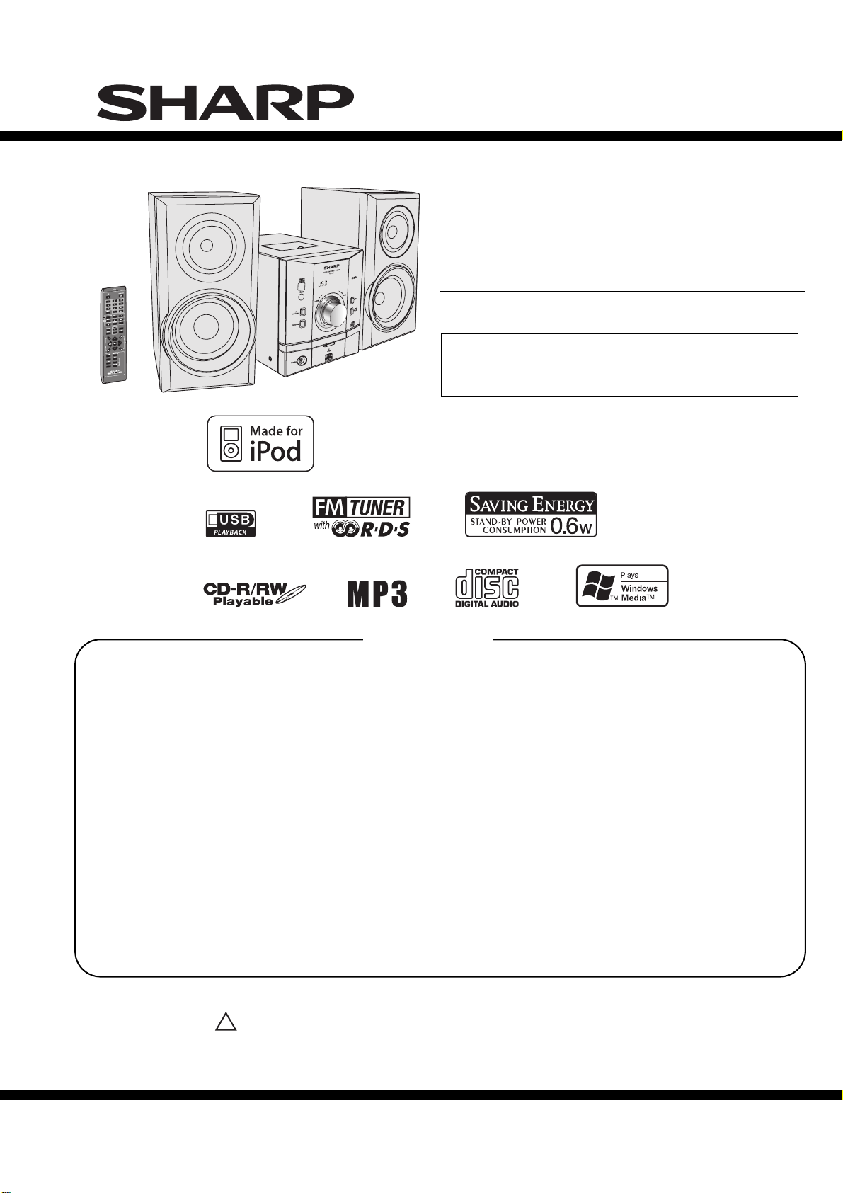
XL-DH20NH
1 – 2
CHAPTER 1. GENERAL DESCRIPTION
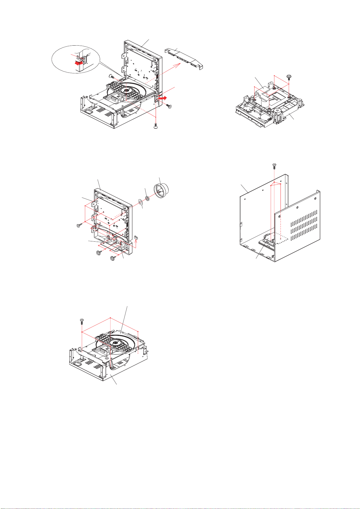
[1] Safety Precaution For Service Manual
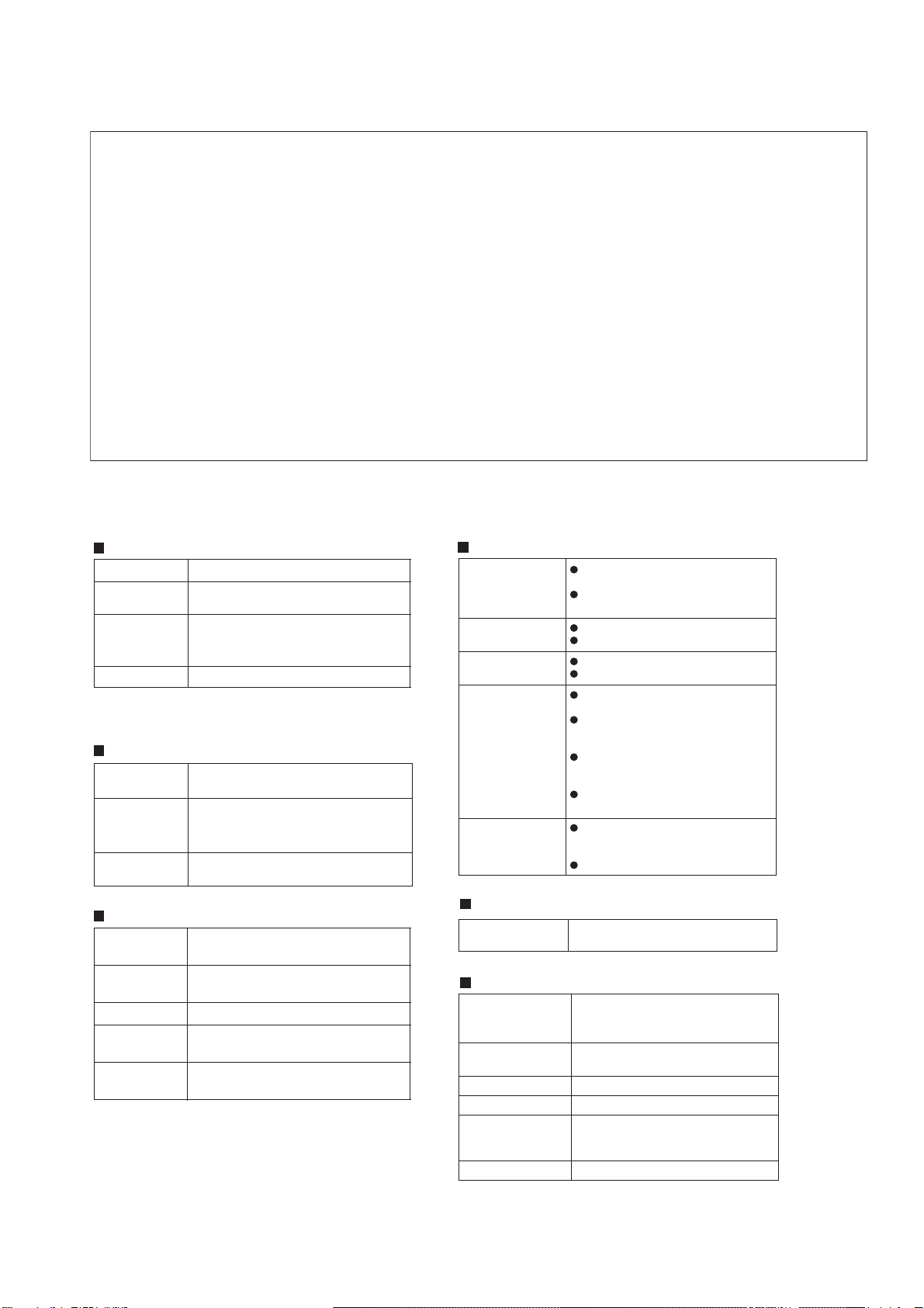
[2] Specifications
This product is classified as a CLASS 1 LASER PRODUCT.
WARNINGS
THE AEL (ACCESSIBLE EMISSION LEVEL) OF LASER POWER OUTPUT FOR THIS MODEL IS SPECIFIED TO
BE LOWER THAN CLASS IREQUIREMENTS. HOWEVER, THE FOLLOWING PRECAUTIONS MUST BE OBSERVED
DURING SERVICING TO PROTECT YOUR EYES AGAINTS EXPOSURE TO THE LASER BEAM.
1- WHEN THE CABINET HAS BEEN REMOVED, THE POWER IS TURNED ON WITHOUT A COMPACT DISC,
AND THE PICKUP IS ON A POSITION OUTER THAN THE LEAD-IN POSITION, THE LASER WILL LIGHT FOR
SEVERAL SECONDS TO DETECT A DISC.
DO NOT LOOK INTO THE PICKUP LENS.
2- THE LASER POWER OUTPUT OF THE PICKUP INSIDE THE UNIT AND REPLACEMENT SERVICE PARTS
HAVE ALREADY BEEN ADJUSTED PRIOR TO SHIPPING.
3- NO ADJUSTMENT TO THE LASER POWER SHOULD BE ATTEMPTED WHEN REPLACING OR SERVICING
THE PICKUP.
4- UNDER NO CIRCUMSTANCES LOOK DIRECTLY INTO THE PICKUP LENS AT ANY TIME.
5- CAUTION - USE OF CONTROLS OR ADJUSTMENTS, OR PERFORMANCE OF PROCEDURES OTHER THAN
THOSE SPECIFIED HEREIN MAY RESULT IN HAZARDOUS RADIATION EXPOSURE.
USB
Tuner
Speaker
USB host
interface Complies with USB 1.1 (Full
Speed)/ 2.0 Mass Storage Class.
Support Bulk only and CBI
protocol.
Support file MPEG 1 Layer 3
WMA (Non DRM)
Bitrate support MP3 (32 ~ 320 kbps)
WMA (64 ~ 160 kbps)
Other Maximum total number of MP3/
WMA files is 65280.
Maximum total number of folders
is 255 INCLUSIVE of root
directory.
The ID3TAG information
supportedareTITLE,ARTISTand
ALBUM only.
Supports ID3TAG version 1 and
version 2.
File system
support Support USB devices with
Microsoft Windows/DOS/FAT 12/
FAT 16/ FAT 32.
2 kbyte block length for sector.
Frequency range FM: 87.5 - 108 MHz
AM: 522 - 1,620 kHz
Type
Maximum input
power 50 W
Rated input power 25 W
Impedance 6 ohms
Dimensions
Weight 1.98 kg (4.36 lbs.)/each
General
Power source AC 220 - 240V ~ 50/60 Hz
Power
consumption Power on: 45 W
Power stand-by: 0.6 W (*)
Dimensions Width: 155 mm (6-3/32")
Height: 178 mm (7-1/64")
Depth: 243 mm (9-9/16")
Weight 2.12 kg (4.67 lbs.)
( * ) This power consumption value is obtained when the
main unit is in stand-by mode without iPod charging.
Amplifier
Output power MPO: 50 W (25W + 25 W) (10%T.H.D.)
RMS: 50 W (25 W + 25W) (10% T.H.D.)
Output
terminals Speakers: 6 ohms
Headphones: 16 - 50 ohms
(recommended: 32 ohms)
Input terminals AUX IN (Analogue input):
500 mV/47 k ohms
CD player
Type Single disc multi-play compact disc
player
Signal
readout Non-contact, 3-beam
semiconductor laser pickup
D/A converter Multi bit D/A converter
Frequency
response 20 - 20,000 Hz
Dynamic
range 90 dB (1 kHz)
2-way 2-speaker system
5 cm (2") tweeter
10 cm (4") woofer
Width: 132 mm (5-13/64")
Height: 260 mm (10-15/64")
Depth: 171.5 mm (6-49/64")
1 – 1