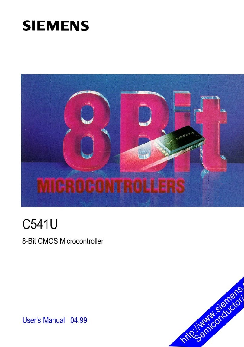
Siemens AP164601 User manual

Semiconductor Group 1998-02, Rel. 1.0
Microcontrollers
ApNote AP164601
oadditional file
APX164601.EXE available
Port Initialization and Direction Control
This Application Note discusses various aspects of the initialization of port pins as
outputs: effects of single Bit and Bit Field (BFLDL/H) instructions, ports with bit
protection, initialization of alternate output functions, effects of interrupts during port
initialization, and bitfield function in C compilers
Author: Christoph Meinhold / HL DC AT

Port Initialization
and Direction Control
Semiconductor Group 2 of 7 AP164601 1998-02
1 Port Structure - Overview..............................................................................................3
2 Initialization of Single Port Pins as Outputs................................................................3
2.1 Configuration as General Purpose Outputs .................................................................3
2.2 Configuration of Alternate Output Function ..................................................................5
2.3 Configuration of CAPCOM Pins....................................................................................5
3 Initialization of several Port Pins on the same Port ...................................................5
AP164601 ApNote - Revision History
Actual Revision : Rel. 1.0 Previous Revison: Rel. 0.0
Page of
Actual Rel. Page of
prev. Rel. Subjects changes since last release)
7 7 Example for bit field function in C added

Port Initialization
and Direction Control
Semiconductor Group 3 of 7 AP164601 1998-02
1 Port Structure - Overview
Each of the general purpose I/O ports (except Port 5) consists of a Port data register Px
and a Port Direction register DPx. Each port pin is individually bit-addressable and
configurable. The value in the direction register determines whether the corresponding
port pin is configured as output (output driver(s) enabled) or input (pin is in high
impedance state). Some of the ports have an additional Open Drain Control register ODPx
(not implemented in 8xC166 devices). When in open drain output mode, only a logic ’0’ is
actively driven, while a logic ’1’ must be provided by an external pullup.
When reading a pin which is configured as input, the logic state of the pin is read, while
reading a pin configured as output returns the value of the corresponding bit in the port
data register. When writing to a port, always the port data register is written to.
After reset, all I/O port pins are configured as inputs, and the port data registers Px
contain the default value 0000h. Port pins which are used as address and/or data bus
from reset on, including the BHE#/WRH# signal (P3.12) for 16-bit data bus modes, are
configured automatically by hardware. All other pins have to be configured by software
when they are to be used as outputs.
2 Initialization of Single Port Pins as Outputs
2.1 Configuration as General Purpose Outputs
When a port pin is to be used as general purpose output, first the initial output value
should be written to the port data register, and then the direction of this pin should be set
to output to achieve a defined transition from the floating state to the actively driven state.
This could be done, e.g. for a Port 1 pin, via the following instruction sequence:
BSET P1.7 ; set initial ouput value (syntax for 8xC166 microcontrollers)
BSET DP1.7 ; set direction to output
NOP ; or other instruction which does not access P1
BSET P1L.7 ; set initial ouput value (syntax for other C166 microcontrollers)
EXTR #1
BSET DP1L.7 ; set direction to output
NOP ; or other instruction which does not access P1
Note 1: When the direction of a port pin has been changed, the next instruction should
not yet access this pin, since the modification is not effective until after the instruction
following the modifying instruction. Otherwise, the next instruction may still read the pin
status instead of the port data register value, or vice versa, depending whether the
direction has been switched from input to output, or vice versa (pipeline effect, see also
following examples, and section ’Particular Pipeline Effects’ in respective User’s Manual,
e.g. C167 Derivatives User’s Manual, V2.0, p. 4-7).
Port Initialization
and Direction Control
Semiconductor Group 4 of 7 AP164601 1998-02
Note 2: When a port is in the initial input configuration after reset, and no external source
is driving the pins to defined logic levels, it is not guaranteed that the reset value ’0’ for a
specific bit will still be in the port data register after a read-modify-write operation has
been performed on any bit of this port. This applies to explicit AND/OR masking as well
as to Bit and Bit Field instructions, which are implicit read-modify-write instructions and
always perform a complete word access on a port.
The reason for this effect is that any read access on port pins configured as inputs returns
the logic levels of the individual pins. Therefore, when the value in the port data register is
different from the logic level at the pin, the value in the port data register may
unintentionally be overwritten by a read-modify-write operation. This may also result in
sporadic problems when the level at the input pin is floating to random logic levels.
For ports which are associated with the CAPCOM/CAPCOM2 or PWM unit (P2, P7, P8), a
specific bit protection mechanism has been implemented which prevents single bits
which are modified by the on-chip periperal units from unintentionally being overwritten by
a bit read-modify-write sequence via Bit and Bit Field instructions (see section ’Protected
Bits’ and ’Bit-Handling and Bit-Protection’ in respective User’s Manual, e.g. C167
Derivatives User’s Manual, V2.0, p. 2-17 and p. 4-9).
It is therefore advised to always set the port data register and the port direction register (at
least for all ports without bit protection) as one unit in two consecutive instructions.
In case interrupts could occur after the instruction which writes to the port data register,
and in the interrupt service routine read-modify-write instructions are executed which also
access this port, it is additionally recommended to temporarily disable interrupts, e.g.
; (syntax for 8xC166 microcontrollers)
BFLDH PSW, #0F0h, #0F0h ; set PSW.ILVL to highest priority level
NOP ; Note: NMI# may still interrupt this sequence
BSET P1.7 ; set initial ouput value
BSET DP1.7 ; set direction to output
BFLDH PSW, #0F0h, #00h ; restore previous priority
; (syntax for other C166 microcontrollers)
ATOMIC #2 ; disable interrupts and class A traps for 2 instruction cycles
BSET P1L.7 ; set initial ouput value
EXTR#1
BSET DP1L.7 ; set direction to output
NOP ; or other instruction which does not access P1
This procedure is also recommended when a port pin is used in a bidirectional manner,
i.e. when its direction is dynamically changed from input to output.

Port Initialization
and Direction Control
Semiconductor Group 5 of 7 AP164601 1998-02
2.2 Configuration of Alternate Output Function
In order to use an alternate output function of a Port 3 pin, its direction must be set to
output AND the corresponding port data register bit must contain a ‘1’. Otherwise, the
alternate output function is not enabled and the pin will be stuck at ‘0’ (see figure of Port 3
pins in chapter 'Parallel Ports' in respective User's Manual, e.g. C167 Derivatives User's
Manual, V2.0, p. 6-18). Configuration of the WR# signal which is an alternate output
function of P3.13 on 8xC166 microcontrollers or SSC shift clock output on most other
C166 microcontrollers could be performed as follows:
BSET P3.13 ; enable WR#/SCLK as alternate output function of P3.13,
; initial level is inactive high
BSET DP3.13 ; set direction to output
NOP ; or other instruction which does not access P3
Note that when a port data register still contains its reset value 0000h, and the direction of
a pin is set to output before the corresponding bit in the port data register is set to ‘1’, a
low level will appear at the pin. For P3.13/WR# of 8xC166 microcontrollers in particular,
this low level will be regarded as write strobe by external memory devices, and
unexpected results may occur.
2.3 Configuration of CAPCOM Pins
When a Port 2 pin is to be used as compare signal output (alternate function) for the
CAPCOM unit of 8xC166 microcontrollers (respectively Port 7 and Port 8 for CAPCOM2
unit on other C166 microcontrollers), it is not required to write a ‘1’ into the corresponding
bit of the port data register. It is only required to set the direction to output.
3 Initialization of several Port Pins on the same Port
When several port pins are to be configured as outputs on the same port, the port data
register should be programmed before the direction of the selected port pin is set to
output. This is preferably done using MOV or Bit Field instructions.
When for example the alternate function of P3.13 shall be used (WR# function on 8xC166
microcontrollers, SSC shift clock output SCLK on most other C166 microcontrollers), and
P3.10 shall be used as transmit data output TxD0, this could be done with the following
instruction sequence:
BFLDH P3,#24h,#24h ; set P3.13/WR#/SCLK and P3.10/TxD0 to '1'
BFLDH DP3,#24h,#24h ; switch direction to output
NOP ; or other instruction which does not access P3

Port Initialization
and Direction Control
Semiconductor Group 6 of 7 AP164601 1998-02
However, the following sequence is not recommended:
BSET P3.13 ; set P3.13/WR#/SCLK to ’1’
BSET DP3.13 ; set direction of P3.13 to output
BSET P3.10 ; set P3.10/TxD0 to ’1’
; CAUTION: P3.13 is not yet switched to output when this instruction reads P3
; (pipeline effect)
; ==> P3.13 value read from pin, maybe undefined
; ==> P3.13 SFR value may be overwritten with pin value by this instruction
; ==> no WR# strobe or shift clock may be output
BSET DP3.10 ; set direction of P3.10 to output
...
Therefore, when several pins are to be initialized with single bit instructions on the same
port (and this port does not have bit protection), it is important that an instruction which
does not access this port is placed between two BSET Px / BSET DPx instruction pairs,
and in general after each instruction which has modified the port direction, as follows:
BSET P3.13 ; set P3.13/WR#/SCLK to ’1’
BSET DP3.13 ; set direction of P3.13 to output
NOP ; or other instruction which does not access P3
BSET P3.10 ; set P3.10/TxD0 to ’1’
BSET DP3.10 ; set direction of P3.10 to output
NOP ; or other instruction which does not access P3
Or, on C level:
_pubit (P3,13);
_pubit (DP3,13);
_nop();
_pubit (P3,10);
_pubit (DP3,10);
_nop();
When several pins in different bytes of a port (without bit protection) are to be initialized
with Bit Field instructions, also care must be taken that subsequent instructions will read
the correct port status, e.g.
BFLDH P3,#24h,#24h ; set P3.13/WR#/SCLK and P3.10/TxD0 to ’1’
BFLDH DP3,#24h,#24h ; switch P3.13 and P3.10 to output
NOP ; or other instruction which does not access P3
BFLDL P3,#0Ah,#0Ah ; set P3.1/T6OUT and P3.3/T3OUT to ’1’
BFLDL DP3,#0Ah,#0Ah ; switch P3.1 and P3.3 to output
NOP ; or other instruction which does not access P3

Port Initialization
and Direction Control
Semiconductor Group 7 of 7 AP164601 1998-02
As discussed before, if interrupts can occur after the instruction which modifies the port
data register, and in the interrupt service routines read-modify-write instructions are
executed which also access this port, it is additionally recommended to temporarily disable
interrupts.
The built-in bitfield function of some C compilers allows to modify up to 16 bits of a bit-
addressable word. When this function is used, care mut be taken when several pins in
different bytes of a port are initialized, since the compiler might generate consecutive
BFLDL/H instructions which access the same port, e.g.:
_bfld (P3, 0x240A, 0x240A); Keil-Syntax: _bfld_ (...
_bfld (DP3, 0x240A, 0x240A);
This instruction sequence may result in the following assembler instruction sequence:
BFLDH P3,#24h,#24h ; set P3.13/WR#/SCLK and P3.10/TxD0 to ’1’
BFLDL P3,#0Ah,#0Ah ; set P3.1/T6OUT and P3.3/T3OUT to ’1’
; CAUTION: P3.13 and P3.10 are still inputs when this instruction reads P3
; ==> P3.13 and P3.10 values read from pin, maybe undefined
; ==> P3.13 and P3.10 SFR values may be overwritten with pin values
; ==> no WR# strobe or shift clock may be output
BFLDH DP3,#24h,#24h ; switch P3.13 and P3.10 to output
BFLDL DP3,#0Ah,#0Ah ; switch P3.1 and P3.3 to output
Therefore, this bitfield function should not be used
- in particular when Port 3 pins are initialized
- on 8xC166 microcontrollers for Port 1 and Port 0 pins, since these ports are
implemented as 16-bit wide ports, while on other C166 microcontrollers, these ports
are implemented as two 8-bit wide ports each, like most other I/O ports
For ports with bit protection (Port 2, 7, 8), these types of problems will not occur.
Table of contents
Other Siemens Microcontroller manuals
Popular Microcontroller manuals by other brands

Lattice Semiconductor
Lattice Semiconductor MachXO2 Pico quick start

Infineon Technologies
Infineon Technologies XMC4000 Application Kit user manual

Xsens
Xsens MTi 1-series user manual

Globalstar
Globalstar STX3 quick start guide

Atop
Atop SE59XX-SDK user manual

Silicon Laboratories
Silicon Laboratories EFM32JG1 Reference manual