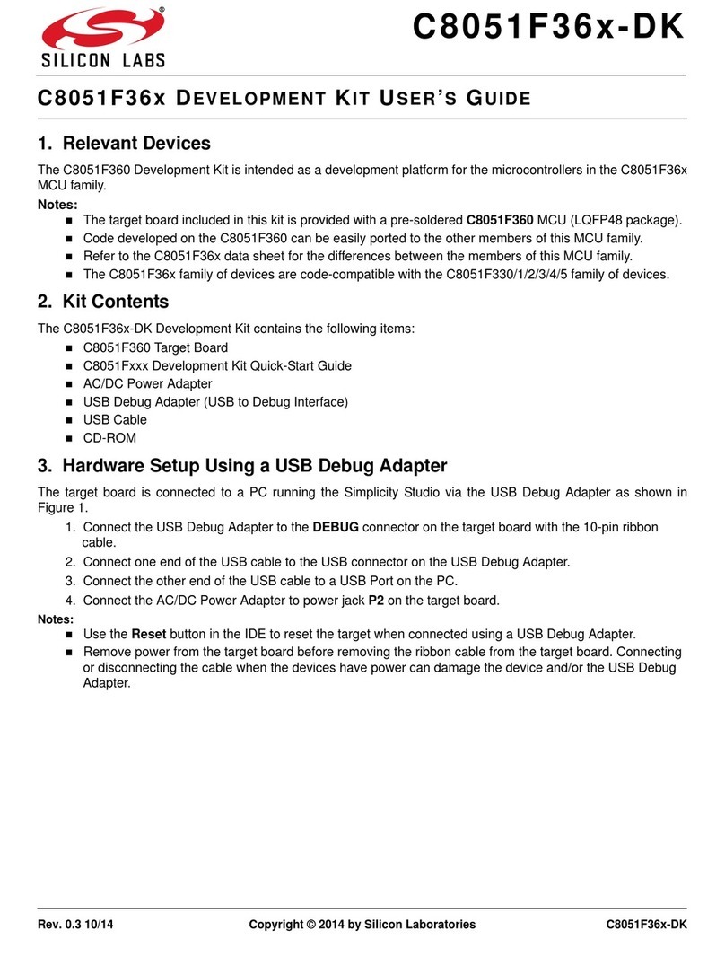
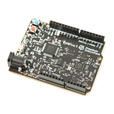
SiFive FE310-G000 User manual

SiFive FE310-G000 Manual
Version 1.0.1
c
SiFive, Inc.

2SiFive FE310-G000 Manual, Version 1.0.1

SiFive FE310-G000 Manual
Proprietary Notice
Copyright c
2016, SiFive Inc. All rights reserved.
Information in this document is provided “as is”, with all faults.
SiFive expressly disclaims all warranties, representations and conditions of any kind, whether ex-
press or implied, including, but not limited to, the implied warranties or conditions of merchantabil-
ity, fitness for a particular purpose and non-infringement.
SiFive does not assume any liability rising out of the application or use of any product or circuit, and
specifically disclaims any and all liability, including without limitation indirect, incidental, special,
exemplary, or consequential damages.
SiFive reserves the right to make changes without further notice to any products herein.
Release Information
Version Date Changes
1.0.1 December 20, 2016 Add QFN48 Package Pinout,
add Configuration String, re-
name chip to FE310-G000
1.0 November 29, 2016 HiFive1 release
i

ii SiFive FE310-G000 Manual, Version 1.0.1

Contents
SiFive FE310-G000 Manual i
1 Introduction 1
1.1 BlockDiagram...................................... 1
1.2 E31 Coreplex Configuration . . . . . . . . . . . . . . . . . . . . . . . . . . . . . . 1
1.3 CLINT .......................................... 2
1.4 PLIC ........................................... 2
1.5 JTAGConnections ................................... 2
1.6 DebugModule...................................... 2
1.7 Quad-SPIFlash..................................... 3
1.8 GPIOComplex ..................................... 3
1.9 Always-On(AON)Block ................................ 3
1.10 PowerSupply ...................................... 3
2 FE310-G000 Pins 5
2.1 FE310-G000Pinmux .................................. 5
3 FE310-G000 Memory Map 7
4 FE310-G000 Interrupts 9
5 FE310-G000 Boot 11
5.1 Non-volatile Code Options . . . . . . . . . . . . . . . . . . . . . . . . . . . . . . . 11
5.1.1 GateROM(GROM) ............................. 11
5.1.2 MaskROM(MROM) ............................. 11
5.1.3 One-Time Programmable (OTP) Memory . . . . . . . . . . . . . . . . . 11
5.1.4 Quad SPI Flash Controller (QSPI) . . . . . . . . . . . . . . . . . . . . . 12
5.2 BootScenarios ..................................... 12
iii

Chapter 1
Introduction
The FE310-G000 is the first Freedom E300 SoC, and forms the basis of the HiFive1 development
board for the Freedom E300 family. The FE310-G000 is built around the E31 Coreplex instantiated
in the Freedom E300 platform, and the E3 Coreplex Series and Freedom E300 Platform manuals
should be read together with this manual. This manual only describes the specifics of the FE310-
G000.
FE310-G000 is fabricated in the TSMC CL018G 180nm process.
Block Diagram
Figure 1.1 shows the overall block diagram of FE310-G000. FE310-G000 contains an E31-based
Coreplex, a selection of flexible I/O peripherals, a dedicated off-chip Quad-SPI flash controller
for execute-in-place, 8 KiB of in-circuit programmable OTP memory, 8 KiB of mask ROM, clock
generation, and an always-on (AON) block including a programmable power-management unit
(PMU).
E31 Coreplex Configuration
The core is configured to support the RV32IMAC ISA options.
The branch predictor configuration has 40 branch-target buffer (BTB) entries, 128 branch-history
(BHT) entries, and a two-entry return-address stack (RAS).
The integer multiplier completes 8 bits per cycle, so takes up to four clock cycles for a single 32×32
multiply operation.
The integer divider completes one bit per clock cycle, with an early out.
The instruction cache is a 16 KiB two-way set associative with 32-byte lines.
The data SRAM is 16 KiB.
The system mask ROM is 8 KiB in size and contains simple boot code. The system ROM also
holds the platform configuration string and debug ROM routines.
1

2SiFive FE310-G000 Manual, Version 1.0.1
FE310G-0000 GPIO Complex
Always-On Domain
P-Bus: TileLink B32 D32
QSPI0
Real-Time Clock
Platform-Level
Interrupt Control
TAPC
Debug Module
Debug RAM (28B)
Instruction Fetch
RV32IMAC
Branch Prediction
Inst. Decompressor
Instruction Buffer
M
MLoad/Store
dip
eip
lip
Instruction Cache
(16KiB, 2-way)
Instruction Cache Refill M
OTP (8KiB)
Data SRAM (16KiB)
UART0
QSPI1
M
JTAG
1.8V AON Core
erst_n
QSPI Flash
GPIO
Multiplier/Divider
Watchdog
Coreplex-Local
Interrupt Control
Real-Time Clock Ticks
Backup Registers
PMU
Reset Unit
dwakeup_n
1.8V AON Pads
vddpaden
LFROSC
psdaon*
Mask ROM (8KiB)
Clock Generation
HFXOSC
PLL
HFROSC
vddpll
vsspll
hfxoscin
hfxoscout
UART1
PWM0 (16-bit)
PWM1 (8-bit)
QSPI2
C-Bus: TileLink B32 D32
A-Bus: TileLink B4 D32
M
hfclkrst
rtccmpip
wdogcmpip
Global
Interrupts
1.8V MOFF Core
3.3V MOFF Pads
psd*
E31 Coreplex
Core Reset Sync corerst
Figure 1.1: FE310-G000 top-level block diagram.
CLINT
The Coreplex-Local Interrupt Controller (CLINT) supports the standard timer and software inter-
rupts.
PLIC
The platform-level interrupt controller (PLIC) receives interrupt signals from the peripheral devices
and prioritizes these for service by the core. The PLIC has 52 inputs, each supporting 7 pro-
grammable priority levels.
JTAG Connections
A four-wire 1149.1 JTAG connection is used to connect the external debugger to the internal debug
module.
Debug Module
The debug module is accessed over JTAG, and has support for two programmable hardware
breakpoints. The debug RAM has 28 bytes of storage.

Copyright c
2016, SiFive Inc. All rights reserved. 3
Quad-SPI Flash
A dedicated quad-SPI (QSPI) flash interface is provided to hold code and data for the system.
The QSPI interface supports burst reads of 32 bytes over TileLink to accelerate instruction cache
refills. The QSPI can be programmed to support eXecute-In-Place modes to reduce SPI command
overhead on instruction cache refills. The QSPI interface also supports single-word data reads
over the primary TileLink interface, as well as programming operations using memory-mapped
control registers.
GPIO Complex
The GPIO complex manages the connection of digital I/O pads to digital peripherals, including
SPI, UART, and PWM controllers, as well as for regular programmed I/O operations. FE310-G000
has two additional QSPI controllers in the GPIO block, one with four chip selects and one with
one. FE310-G000 also has two UARTs. FE310-G000 has three PWM controllers, two with 16-bit
precision and one with 8-bit precision.
Always-On (AON) Block
The AON block contains the reset logic for the chip, an on-chip low-frequency oscillator, a watch-
dog timer, connections for an off-chip low-frequency crystal oscillator, the real-time clock, a pro-
grammable power-management unit, and 16×32-bit backup registers that retain state while the
rest of the chip is powered down.
The AON can be instructed to put the system to sleep. The AON can be programmed to exit sleep
mode on a real-time clock interrupt or when the external digital wakeup pin, dwakeup n, is pulled
low. The dwakeup n input supports wired-OR connections of multiple wakeup sources.
Power Supply
FE310-G000 requires two dedicated power rails providing 1.8 V power to the always-on block and
core logic, and 3.3 V to the I/O pads.

4SiFive FE310-G000 Manual, Version 1.0.1

6SiFive FE310-G000 Manual, Version 1.0.1
Table 2.1: FE310-G000 Pin Hardware I/O Functions
Pin Number IOF0 IOF1
0 PWM0 0
1 PWM0 1
2 QSPI1:SS0 PWM0 2
3 QSPI1:SD0/MOSI PWM0 3
4 QSPI1:SD1-MISO
5 QSPI1:SCK
6 QSPI1:SD2
7 QSPI1:SD3
8 QSPI1:SS1
9 QSPI1:SS2
10 QSPI1:SS3 PWM2 0
11 PWM2 1
12 PWM2 2
13 PWM2 3
14
15
16 UART0:RX
17 UART0:TX
18
19 PWM1 1
20 PWM1 0
21 PWM1 2
22 PWM1 3
23
24 UART1:RX
25 UART1:TX
26 QSPI2:SS
27 QSPI2:SD0/MOSI
28 QSPI2:SD1/MISO
29 QSPI2:SCK
30 QSPI2:SD2
31 QSPI2:SD3

Chapter 3
FE310-G000 Memory Map
Table 3.1 enumerates the peripherals included in FE310-G000 and where they are located in the
memory map.
Base Top Description
0x0000 0000 0x0FFF FFFF (see E3 Coreplex Manual)
0x0002 0000 0x0002 1FFF On-chip OTP read (≤8 KiB)
0x1000 0000 0x1000 7FFF Always-On (AON)
0x1000 8000 0x1000 FFFF Power, Reset, Clock, Interrupts (PRCI)
0x1001 0000 0x1001 0FFF On-chip OTP control
0x1001 1000 0x1001 1FFF Reserved
0x1001 2000 0x1001 2FFF GPIO0 with 32 GPIO
0x1001 3000 0x1001 3FFF UART0
0x1001 4000 0x1001 4FFF Off-Chip QSPI0 Control
0x1001 5000 0x1001 5FFF PWM0 (8 bit timer with 4 cmp)
0x1001 6000 0x1002 2FFF Reserved
0x1002 3000 0x1002 3FFF UART1
0x1002 4000 0x1002 4FFF Off-Chip QSPI1 Control (4CS)
0x1002 5000 0x1002 5FFF PWM1 (16bit timer with 4 cmp)
0x1002 6000 0x1003 3FFF Reserved
0x1003 4000 0x1003 4FFF Off-Chip QSPI2 Control (1CS)
0x1003 5000 0x1003 5FFF PWM2 (16bit timer with 4 cmp)
0x1003 6000 0x1FFF FFFF Reserved
0x2000 0000 0x3FFF FFFF Off-chip QSPI0 flash read (1CS)
(512 MiB)
0x4000 0000 0x7FFF FFFF Reserved
0x8000 0000 0x8000 3FFF Instruction and Data SRAM (16 KiB)
0x8000 4000 0xFFFF FFFF Reserved
Table 3.1: FE310-G000 Peripherals Map
7

8SiFive FE310-G000 Manual, Version 1.0.1

Chapter 4
FE310-G000 Interrupts
Table 4.1 lists the PLIC interrupt sources in FE310-G000. The PLIC on FE310-G000 has a 3-bit
programmable interrupt priority field on each interrupt source.
Interrupt Number Source
0No Interrupt
1 wdogcmp
2 rtccmp
3 uart0
4 uart1
5 qspi0
6 qspi1
7 qspi2
8 gpio0
...
39 gpio31
40 pwm0cmp0
...
44 pwm0cmp3
45 pwm1cmp0
...
48 pwm1cmp3
49 pwm2cmp0
...
52 pwm2cmp3
Table 4.1: FE310-G000 Interrupt Sources
9

10 SiFive FE310-G000 Manual, Version 1.0.1

Chapter 5
FE310-G000 Boot
This chapter describes the operation of FE310-G000 during the boot process.
Non-volatile Code Options
There are four possible sources of non-volatile memory from which code can be initially fetched
on a FE310-G000 system: Gate ROM, Mask ROM, OTP, and off-chip SPI flash.
Gate ROM (GROM)
The debug ROM is built from gate ROM and contains code for the debug interrupt handler that
jumps to debug RAM, as well as code to wait for a debug interrupt.
The default value of mtvec, the trap vector base address, is set to 0x0. Fetches from address 0x0
are hardwired to return 0, which is an illegal instruction, causing another trap, hence causing the
processor to spin in a trap loop on any fetch to address 0.
The trap loop is used to hold the processor when waiting for the debugger to download code to be
executed. The debugger can issue a debug interrupt, which causes the processor to jump to the
debug interrupt handler in debug ROM, which in turn jumps to the code written to the debug RAM.
The debug RAM code can be used to bootstrap download of further code.
Mask ROM (MROM)
MROM is fixed at design time, and is located on the peripheral bus on FE310-G000 but instructions
fetched from MROM are cached by the E31 core’s I-cache. The MROM contains an instruction at
address 0x1000 which jumps to the OTP start address at 0x2 0000.
One-Time Programmable (OTP) Memory
The OTP is located on the peripheral bus, with both a control register interface to program the
OTP, and a memory read port interface to fetch words from the OTP. Instruction fetches from the
OTP memory read port are cached in the E31 core’s instruction cache.
The OTP needs to be programmed before use and can only be programmed by code running on
the E31 core. The OTP bits contain all 0s prior to programming.
11

12 SiFive FE310-G000 Manual, Version 1.0.1
Quad SPI Flash Controller (QSPI)
The dedicated QSPI flash controller connects to external SPI flash parts that are used for execute-
in-place code. SPI flash is not available in certain scenarios such as package testing or board
designs not using SPI flash (e.g., just using on-chip OTP).
Off-chip SPI parts can vary in number of supported I/O bits (1, 2, or 4). SPI flash bits contain all
1s prior to programming.
Boot Scenarios
Table 5.1 outlines the possible scenarios under which the system will be booted.
MROM OTP QSPI Boot strategy
N N N Spin and wait for debugger to download code into SRAM. Can only
execute code from SRAM.
N N U Spin and wait for debugger to download SPI flash programming code
into SRAM, and program flash from SRAM-based code.
N N P Jump to SPI code and execute-in-place through I-cache.
N U X Spin and wait for debugger to download OTP programming code into
SRAM, and program OTP from SRAM-based code.
N P X Jump to OTP code and execute using I-cache.
P N N Spin and wait for debugger to download application code into SRAM.
Can use ROM library routines.
P N U Spin and wait for debugger to download SPI flash programming code
into SRAM, but can use ROM library routines.
P N P Jump to SPI code and execute-in-place through I-cache. Code can use
ROM library routines.
P U X Spin and wait for debugger to download OTP flash programming code
into SRAM, but can use ROM library routines.
P P X Jump to OTP code and execute using I-cache.
Table 5.1: Boot process for various non-volatile code storage scenarios. The letter N indicates
not available (either not present or not functioning), U indicates present but unprogrammed, P
indicates present and programmed, X indicates don’t care.
The three distinct possible boot actions are “spin and wait”, “jump to OTP”, and “jump to SPI”. The
logic to select one of these actions depends on both the supported/working hardware on the chip
and the dynamic state of the system.
Reset and Trap Vectors
The reset PC value is affected by the IP enable pads, as shown below:
When reset is directed to start fetching from 0x0000 0000, the core will enter a trap loop, repeatedly
fetching 0 (illegal instruction) from address 0x0.
When reset is directed to start fetching from the QSPI, if the first word in the external QSPI flash
has not been programmed it will contain all 1s, which is an illegal instruction. The core will then

Copyright c
2016, SiFive Inc. All rights reserved. 13
psdmaskromen psdotpen psdqspien Reset PC Description
X 0 0 0x0000 0000 Cause trap loop.
X 0 1 0x2000 0000 Jump to QSPI.
0 1 X 0x0002 0000 Jump directly to OTP.
1 1 X 0x0000 1000 Correct operation, jump to ROM.
trap to the initial 0x0 vector and enter a trap loop as before. If the QSPI has been programmed,
the system will continue to execute boot code from the flash.
When reset is directed to start fetching from OTP, if the first word in the OTP has not been pro-
grammed, it will contain all 0s, which is an illegal instruction, again causing the core to spin and
wait for the debugger at the initial trap vector. If the OTP has been programmed, the core will begin
executing core out of the OTP.
If all components are working correctly, FE310-G000 will perform like a production E300 chip by
fetching the first instruction from 0x1000. For FE310-G000 the instruction stored there jumps
straight to OTP at 0x2 0000, and will either enter trap loop if the OTP is not programmed, or start
running the OTP code.

14 SiFive FE310-G000 Manual, Version 1.0.1
Other manuals for FE310-G000
2
Table of contents
Other SiFive Microcontroller manuals
Popular Microcontroller manuals by other brands

Texas Instruments
Texas Instruments MSP-EXP430FR5969 user guide

Pasternack
Pasternack PEM003-KIT user guide

Luminus Devices
Luminus Devices PhlatLight DK-125M Series manual

Texas Instruments
Texas Instruments SimpleLink CC2652RB manual

mikroElektronika
mikroElektronika CLICKER 2 STM32 manual

Atmel
Atmel UC3 Series manual