SightLine ICD-4000-OEM User manual

© SightLine Applications, Inc. i
ICD-4000-OEM
2022-06-08
Exports: Export Summary Sheet
EULA: End User License Agreement
Web: sightlineapplications.com
1Overview................................................................1
1.1 Additional Support Documentation.......................1
1.2 Sightline Software Requirements ..........................1
2Safe Device Handling..............................................1
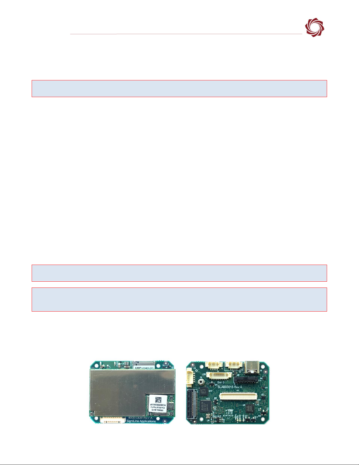
34000-OEM Overview..............................................1
3.1 4000-OEM Specifications.......................................2
3.2 Interface Protocol ..................................................2
3.3 Functional Block Diagram ......................................2
3.4 Customer Integration - Key Points.........................3
4Thermal Management ...........................................3
4.1 Heatsink Guidelines ...............................................3
4.2 Gap Pads ................................................................3
4.2.1 Gap Pads SOM Cover .............................................3
4.2.2 Gap Pads Without SOM Cover...............................4
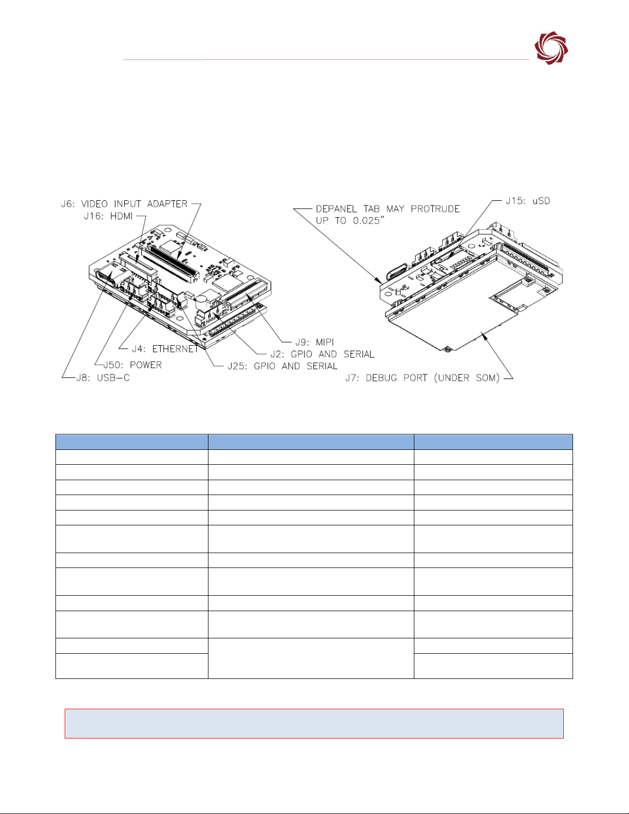
5Connector Descriptions..........................................4
5.1 Connector J2: Serial Port / GPIO ...........................5
5.2 Connector J4: Ethernet 10/100..............................5
5.3 Connector J6: 3000/4000 Video Adapter Input ....5
5.4 Connector J7: 4000-DEBUG / Recovery ................6
5.5 Connector J8: USB 3.0 (Type-C)..............................7
5.6 Connector J9: MIPI Port (FFC connector)...............7
5.7 Connector J15: MicroSD.........................................8
5.8 Connector J16: HDMI Output Video (FFC
connector)..............................................................8
5.9 Connector J25: Additional Serial / GPIO................8
5.10 Connector J50: Power Connector ..........................9
6Additional I/O.........................................................9
6.1 LED Summary .........................................................9
6.2 Serial Ports .............................................................9
6.2.1 Serial Port Speed and Data Limits........................10
6.3 GPIO.....................................................................11
7Camera Naming Convention................................11
8Video Input Port J6 Details (Cam 0).....................12
8.1 Adapter boards ....................................................12
8.2 Camera Power Considerations.............................12
8.3 Signal Levels and Lattice Crosslink FPGA .............12
8.4 Supported Standards ...........................................12
8.5 Grayscale Camera Data........................................13
8.6 Synchronization Signals .......................................14
8.7 Camera Resolution and Pixel Clock
Requirements.......................................................14
8.8 Camera Pixel Clock Rate and MIPI Conversion ....14
8.9 Horizontal Blanking Requirements ......................15
8.9.1 Width and Height Requirements .........................16
8.10 Additional FPGA Versions and naming ................16
8.11 Maximum Width and Height................................16
9MIPI Port J9 (Cam 1) ............................................16
10 Camera Input Adapter Board IDs.........................16
11 4000-DEBUG ........................................................17
11.1 Debug Board Specifications .................................17
12 Customer Designed 4000-OEM Boards and Camera
Interface Options .................................................19
12.1 Using the Lattice FPGA.........................................19
12.2 Not Using the Lattice FPGA..................................19
12.3 MIPI Camera Data Acquisition .............................19
13 Questions and Additional Support.......................19
CAUTION: Alerts to a potential hazard that may result in personal injury, or an unsafe practice that causes damage to the equipment
if not avoided
IMPORTANT: Identifies crucial information that is important to setup and configuration procedures.
Used to emphasize points or reminds the user of something. Supplementary information that aids in the use or understanding of the
equipment or subject that is not critical to system use.

ICD-4000-OEM
Revision History
Date
Description
2022-06-07
Clarify camera requirements for pixel clock rate and blanking.
2022-05-27
Added caution note to disconnect the power before connecting or disconnecting cables.
2022-05-24
Revised Pin 1 and Pin 2 on J16 HDMI Output Video (FFC connector) are not for customer use.
2021-04-25
Updated 4000-OEM connector diagram to show DEPANEL tab protrusion.
2022-04-18
Updated BT.1120 support.
2022-03-07
Updated Supported Standards section.
2022-01-27
Removed serial port converter warning for connector J8: USB 3.0 (Type-C).
2021-12-06
Corrected camera naming conventions for connector J8: USB 3.0 (Type-C).
2021-12-01
Updated Linux column in the 4000-OEM Software Cross Reference table.
2021-11-17
Added mating cycle rating to J9 MIPI connector.
2021-10-26
Expanded connector table to include mates with column.
2021-10-14
Added 4000-OEM GPIO table.
2021-09-02
Added Serial Port tables.
2021-05-12
Clarified Lattice FPGA input pixel clock limitations in Pixel Clock Requirements section.
2020-12-15
Moved Camera Input Adapter Board ID table to ICD-3000-4000-Adapter Boards.
2020-12-01
Added section on changing I2C bus speed to support 921K baud camera.
2020-10-23
Updated the following sections: LED Summary, GPIO Summary, Connector J4, Video Output Description, Signal
Levels and Lattice Crosslink FPGA, 8-Bit BT.656, Synchronization Signals, Pixel Clock Requirements.
2020-10-02
Added note that debug port cannot be repurposed.
2020-09-11
Corrected I2C pin designations to match schematic. Add current 400 kHz frequent note to connector J6 pinout table
and connector J9 pinout table.
2020-08-24
Corrected Grayscale bit locations in the Connector J6: 3000/4000 Input Board Table.
2020-08-14
Updated J16 HDMI (FFC connector) table - Pin 1 is the same as Pin 2.
2020-07-20
Corrected HDMI Output connector label in Video Output section.
2020-07-16
Added GPIO numbers to J6 pinout table.
2020-07-08
Added EAN-OEM-Recovery link to 4000-DEBUG section.
2020-06-01
Added maximum width and height of acquired image and ROI.
2020-04-16
Added warning that the 4000-OEM should not be powered through connector J8: USB 3.0 (Type-C).
2020-04-08
Added new section - Customer Designed 4000-OEM Boards and Camera Interface Options.
2020-03-10
Added note that FPGA now supports multiple pixel widths in 3.01 software. Added FPGA Video Resolution and Pixel
Clock Requirements table for 3.01 software.
2020-01-24
Added max voltage, current and power connector notation to pins 55, 57, 59, 61. Corrected power connector label.
2020-01-17
Added more video format details. Add section on FPGA video resolution requirements.
2020-01-14
Added notes on connector J6 data bit locations.
2019-12-14
Corrected MIPI board serial ports to 4,6,7. Add link to MIPI board ICD.
2019-11-26
Corrected I2Creference for connector 6 and connector 9 in Connector Descriptions table and Pin 20 and 21 in MIPI
Port table.
2019-10-17
Added voltage qualification note to specifications.
2019-09-17
Corrected pins in Serial Port / GPIO table for connector J2.
2019-08-09
Changed GPIO label to SW labels. Revised heatsink statement.

ICD-4000-OEM
© SightLine Applications, Inc. 1
1Overview
Describes power requirements, thermal management, interface specifications, and connector pinouts
for the 4000-OEM video processing board.
CAUTION: Any customer modifications to SightLine OEM and adapter boards will void the warranty and can
potentially damage the board. Before attempting any modifications, please contact Support.
1.1 Additional Support Documentation
Additional Engineering Application Notes (EANs) can be found on the Documentation page of the
SightLine Applications website.
The Panel Plus User Guide provides a complete overview of settings and dialog windows located in the
Help menu of the Panel Plus application.
The Interface Command and Control (IDD) describes the native communications protocol used by the
SightLine Applications product line. The IDD is also available as a PDF download on the Documentation
page under Software Support Documentation.
1.2 Sightline Software Requirements
Panel Plus software and firmware versions:
4000-OEM requires Panel Plus and Firmware 3.0.0 and higher.
IMPORTANT: The Panel Plus software version should match the firmware version running on the
board. Firmware and Panel Plus software versions are available on the Software Download page.
2Safe Device Handling
CAUTION: To prevent damage to hardware boards, disconnect the power before connecting or disconnecting cables
including all FFC, FPC, KEL, HDMI, MIPI, and round wire (Molex) cables.
CAUTION: To prevent damage to hardware boards, use a conductive wrist strap attached to a good earth ground.
Before picking up an ESD sensitive electronic component, discharge built up static by touching a grounded bare
metal surface or approved antistatic mat.
34000-OEM Overview
The 4000-OEM has 11 connectors and one microSD card slot. Connectors are used to connect power,
Ethernet, Serial ports, MIPI input, HDMI output, USB3, and digital video in (with the use of a 3000-
adapter board).
Figure 1: 4000-OEM Overview

ICD-4000-OEM
© SightLine Applications, Inc. 2
3.1 4000-OEM Specifications
Revision:
A3 (Initial Release)
Dimensions:
1.496 in x 1.988 in (38 mm x 50.50 mm)
Weight:
Estimate 30 grams
Voltage (VIN):
8 - 15 VDC (12 VDC nom)1
Power:
6 W (For more information on a low power mode to reduce
power by 2-4W, see EAN-Performance and Latency)
Drawing:
4000-OEM
STEP File:
4000-OEM Rev A STEP
Rev History:
Rev A: Initial production release
All 4000-OEM board mounting holes support M2 screws (0.086 dia.).
3.2 Interface Protocol
The 4000-OEM shares the same interface protocol as other SightLine video processing boards. The
protocol is a packet-based command and control interface. The protocol document is available from the
SightLine website.
3.3 Functional Block Diagram
Figure 2: 4000-OEM Hardware Block Diagram
1
A slightly extended input voltage range is possible with some tradeoffs. Contact Support for more information if this is relevant for a
particular application.
1x Serial Port 2x GPIO
Camera
Input Board
CMOS to MIPI
FPGA
I2C IO Expander
Ethernet Port
Magnetics and
ESD Protection
Ethernet PHY
DEBUG Port
μSD Card
INFORCE 6601 SOM
Temp Sensor
Startup and Temp Monitor
Power Conditioning
ESD Protection
USB3.0 Type-C
Controller
Power Input
USB Type-C Port
HDMI
MIPI Port

ICD-4000-OEM
© SightLine Applications, Inc. 3
3.4 Customer Integration - Key Points
✓Provide a sufficient heat sink for the Snapdragon 820 processor and other major components. Close
attention to heatsinking is critical. See the Thermal Management section for more information.
✓Expose Ethernet port (on J4) to an accessible connector for debug, command and control, and
firmware update capability.
✓Expose debug serial port On J7 to an accessible connector for debugging.
✓For in-system recovery, it is recommended to expose the USB programming/debugging port and the
FASTBOOT_RECOVERY switch/button on J7 to a system accessible connector.
✓If you are designing a custom system interface board with the 4000-SOM contact SightLine
Hardware Engineering prior to design for assistance.
4Thermal Management
4.1 Heatsink Guidelines
IMPORTANT: Close attention to heatsinking is critical.
The component temp range for the InForce 6601 SOM and the Ethernet PHY are 0°C to 70°C, all other
components temp range is -40°C to 85°C. All hardware requires some form of mechanical heatsink.
Customers must design a heatsink in conjunction with their system integration effort. It should provide
a direct conducted path to a significant thermal mass (the wall of a gimbal or housing) or use an active
cooling (fans) that has proven to be successful in cases where a full thermal analysis is not performed.
The provided SOM cover aids heatsinking when the provided mechanical interface is a flat plate and is
our baseline. This cover may be removed, and thermal performance improved if a machined heatsink
interface is implemented. STEP files for the heatsink interface are available from SightLine that can
help with heatsink design and integration.
The 4000-OEM typical power consumption is less than 6W @ 12V. System settings provide an option
for a low power mode with no video output but power reduced by 2-4W, see EAN-Performance and
Latency for more information.
IMPORTANT: The internal temperature, reported in Panel Plus, should not exceed +85°C (185°F) or
the SOM processor will start to reduce clock speed and eventually shut down. Internal high
temperatures for extended periods can cause permanent damage.
4.2 Gap Pads
Use some form of thermally conductive material for filling gaps between the hot components and the
heat sink. Examples such as the TGlobal TG-A6200 Ultra Soft Thermal Conductive Pad (6W/mK or
higher) are recommended. The compression of the pad allows for greater mounting tolerances. The
compression of the gap pad also provides additional support for the board and does not require as
much force to maintain contact.
4.2.1 Gap Pads SOM Cover
When integrating the OEM with the SOM cover/heat spreader installed (onto a flat surface heatsink),
use TGlobal TG-A6200-25-40-5.0 (or Sightline PN: SLA-PAD-020-01), Thermal Pad 1.0 x 1.6 x 0.02 inch.

ICD-4000-OEM
© SightLine Applications, Inc. 4
4.2.2 Gap Pads Without SOM Cover
The cover may be removed if a machined heatsink interface is implemented. STEP files for the OEM
with the SOM cover/heat spreader removed are available from SightLine that can help with heatsink
design and integration. Contact Support for more information.
5Connector Descriptions
Figure 3: 4000-OEM Connector Descriptions
Table 1: Connector Descriptions
Connector
Description
Mates with:
J2: Serial Port / GPIO
Serial port 1, GPIO
Molex 5POS Housing, 51021-0500
J4: Ethernet 10/100
Ethernet 10/100Mbps
Molex 4POS Housing, 51021-0400
J6: 3000/4000 Video Adapter Input
Digital video in 0, serial port 2, I2C-1, GPIO
DF12(3.0)-80DS-0.5V(86)
J7: 4000-DEBUG / Recovery *
System recovery and debug serial port
Molex 8 POS Housing, 51021-0800
J8: USB 3.0 (Type-C)
USB 3.0 (type C)
USB Type-C Cable
J9: MIPI Port (FFC connector)
MIPI Port, I2C-3 (Digital Video in 1, serial ports,
w/adapter board)
Sightline Cable SLA-CAB-MIPI-02
J15: MicroSD
MicroSD card slot
NA
J16: HDMI Output Video (FFC
connector)
HDMI Output (FFC)
Sightline Cable SLA-CAB-HD10
J25: Additional Serial / GPIO
Serial port 0 and 3, GPIO
Molex 8POS Housing, 51021-0800
J50: Power Connector
Typical 12VDC (see 4000-OEM Specifications for
min/max)
Molex 4POS Housing, 51021-0400
S2: IO2 SOM
INFORCE SOM. Pinout not included in this ICD.
For customers making custom interface boards,
contact Support.
NA
S3: IO1 SOM
NA
*The debug serial port is exposed on J7 P7-8 and should be reserved for debugging only. Debug serial port is 1.8V TTL.
CAUTION: J4 (Ethernet) and J50 (power) are adjacent 4-pin connectors. DO NOT connect power to the Ethernet
port. Connecting power to the Ethernet port will damage the board.

ICD-4000-OEM
© SightLine Applications, Inc. 5
5.1 Connector J2: Serial Port / GPIO
Connector: Molex 5POS, 53398-0571 Mates with: Molex 5POS Housing, 51021-0500
Table 2: Serial Port / GPIO
Pin
Signal
Description
1
GND
2
TX1
3.3V TTL
3
RX1
3.3V TTL
4
GPIO7 (Linux GPIO_459)
GPIO
5
GPIO8 (Linux GPIO_460)
GPIO
5.2 Connector J4: Ethernet 10/100
Connector: Molex 4POS, 53398-0471 Mates with: Molex 4POS Housing, 51021-0400
Table 3: Ethernet
Pin
Signal
Description
1
TXA_P
TX+
2
TXA_N
TX-
3
TXB_P
RX+
4
TXB_N
RX-
Ethernet supports full duplex.
Supports 10/100BASE-T only.
Ethernet magnetics and Ethernet protection: The 4000-OEM is configured with onboard Ethernet
magnetics and ESD protection. It meets the following IEC standards, IEC 61000-4-2 (ESD) ±30kV
(air), ±30kV (contact) IEC 61000-4-4 (EFT) 40A (5/50ns) IEC 61000-4-5 (Lightning) 40A (8/20μs).
5.3 Connector J6: 3000/4000 Video Adapter Input
Connector: DF12(3.0)-80DP-0.5V(86) Mates with: DF12(3.0)-80DS-0.5V(86)
Column key for notes column below (data bit locations):
Y = luminance CbCr = Chrominance G = Grayscale bits.
Table 4: 4000-OEM (J6) Pinout
Pin
Description
Notes
Pin
Description
Notes
2
NC
1
VIN_ACLK
Pixel Clock
4
Ground
3
Ground
6
VIN_D22
5
VIN_D23
8
VIN_D20
7
VIN_D21
10
VIN_D18
9
VIN_D19
12
VIN_D16
11
VIN_D17
14
Ground
13
Ground
16
VIN_D14
Y6, G14
15
VIN_D15
Y7, G15
18
VIN_D12
Y4, G12
17
VIN_D13
Y5, G13
20
VIN_D10
Y2, G10
19
VIN_D11
Y3, G11
22
VIN_D8
Y0, G8
21
VIN_D9
Y1, G9
24
Ground
23
Ground

ICD-4000-OEM
© SightLine Applications, Inc. 6
(4000-OEM (J6) Pinout table continued)
26
VIN_D6
CbCr6, G6
25
VIN_D7
CbCr7, G7
28
VIN_D4
CbCr4, G4
27
VIN_D5
CbCr5, G5
30
VIN_D2
CbCr2, G2
29
VIN_D3
CbCr3, G3
32
VIN_D0
CbCr0, G0
31
VIN_D1
CbCr1, G1
34
Ground
33
Ground
36
NC
35
NC
38
NC
37
NC
40
NC
39
NC
42
Port ID (out)
See pin notes
41
NC
44
Ground
43
Ground
46
NC
45
VIN_HSYNC
Horizontal Sync
48
NC
47
VIN_VSYNC
Vertical Sync
50
NC
49
VIN_FLD
Field
52
NC
51
VIN_DE
Optional
54
Ground
53
Ground
56
Passthrough ground
55
Passthrough VIN
See J50*
58
Passthrough ground
57
Passthrough VIN
See J50*
60
Passthrough ground
59
Passthrough VIN
See J50*
62
Passthrough ground
61
Passthrough VIN
See J50*
64
Ground
63
Ground
66
TX2
3.3V TTL
65
RX2
3.3V TTL
68
BLSP8_I2C _SDA
I2C-1
67
BLSP8_I2C _SCL
I2C-1 (400 kHz)
70
GPIO1_3000_BRD
GPIO_453
69
GPIO0_3000_BRD
GPIO_452
72
GPIO3_3000_BRD
GPIO_455
71
GPIO2_3000_BRD
GPIO_454
74
GPIO5_3000_BRD
GPIO_457
73
GPIO4_3000_BRD
GPIO_456
76
+3.3V (out)
75
+3.3V (out)
78
Ground
77
Ground
80
+1.8V (out)
79
+1.8V (out)
*Passthrough power available. Max voltage = VIN (See VIN Specifications). Max Current = 1.2A spread across four power and ground pins.
5.4 Connector J7: 4000-DEBUG / Recovery
A debug serial port is exposed on connector J7 and should be used for debugging only.
Connector: Molex 8 POS, 53398-0871 Mates with: Molex 8 POS Housing, 51021-0800
Table 5: 4000-DEBUG
Pin
Description
Pin
Description
2
USB3_P0_HS_D_P
1
USB3_P0_HS_D_N
4
uUSB_VBUS
3
GND
6
VOL_N (FASTBOOT_RECOVERY
switch)
5
QFIL_USB_SELECT
9
BLSP8_UART_RX (1.8V)
7
BLSP8_UART_TX (1.8)
Debug serial port is 1.8V TTL.
Currently there is not a way to repurpose this port for use by an application on the 4000-OEM. Note
that Serial 0 on both the 1500 and 3000 can be repurposed using a silent command. This approach
does not work on 4000-OEM hardware.
See the 4000-DEBUG section for more information.

ICD-4000-OEM
© SightLine Applications, Inc. 7
5.5 Connector J8: USB 3.0 (Type-C)
Connector: Molex 1054500101 Mates with: USB Type-C Cable
Table 6: USB 3.0
Pin
Description
Pin
Description
A1
GND
B1
GND
A2
USB3_TX1_N
B2
USB3_TX2_P
A3
USB3_TX1_N
B3
USB3_TX2_N
A4
P5V
B4
P5V
A5
CC1
B5
CC2
A6
USB3_P1_HS1_D_P
B6
NA
A7
USB3_P1_HS1_D_N
B7
NA
A8
NA
B8
NA
A9
P5V
B9
P5V
A10
USB3_RX2_N
B10
USB3_RX1_N
A11
USB3_RX2_P
A11
USB3_RX1_P
A12
GND
A12
GND
USB 5V output can source 900mA max. 5V is also used for MIPI interface boards connected on J9
with a combined maximum of 1.2A.
CAUTION: Do NOT connect an external 5V power source to the USB-C connector. Damage to the OEM may
occur.
5.6 Connector J9: MIPI Port (FFC connector)
Connector: Hirose 28POS, FH41-28S-0.5SH(050) Mates with: Sightline Cable SLA-CAB-MIPI-02
The mating cycle rating for this connector is 20 cycles.
Table 7: MIPI Port
Pin
Description
Pin
Description
2
D4+
1
GND
4
GND
3
D4-
6
D3-
5
D3+
8
CLK+
7
GND
10
GND
9
CLK-
12
D2-
11
D2+
14
D1+
13
GND
16
GND
15
D1-
18
IO_HOST_OUT0
17
IO_HOST_OUT1
20
CCIO_I2C_SCL (I2C-3, 400 kHz)
19
GND
22
GND
21
CCIO_I2C _SDA (I2C-3)
24
IO_HOST_IN0
23
IO_HOST_IN1
26
VCC_5V
25
VCC_5V
28
GND
27
VCC_5V
Limit power supplied over FFC cable to 6.75 watts (1.35A @5V).

ICD-4000-OEM
© SightLine Applications, Inc. 8
5.7 Connector J15: MicroSD
Push the microSD into place. To eject it push it again. The socket is rated up to 10,000 mating cycles
and has 3.3 mm card eject length.
Recommended microSD card types and previously tested models are discussed in the EAN-File-
Recording document.
5.8 Connector J16: HDMI Output Video (FFC connector)
Connector: Amphenol 20POS, 62674-201121ALF Mates with: Sightline Cable SLA-CAB-HD10
Table 8: HDMI
Pin
Description
Pin
Description
2
HDMI_C_5VOUT*
1
HDMI_C_5VOUT*
4
HDMI_C_DATA
3
HDMI_C_HPD
6
HDMI_C_CEC
5
HDMI_C_CLK
8
GND
7
GND
10
HDMI_TMDS_CLK_C_P
9
HDMI_TMDS_CLK_C_N
12
HDMI_TMDS_TX0_C_N
11
GND
14
GND
13
HDMI_TMDS_TX0_C_P
16
HDMI_TMDS_TX1_C_P
15
HDMI_TMDS_TX1_C_N
18
HDMI_TMDS_TX2_C_N
17
GND
20
GND
19
HDMI_TMDS_TX2_C_P
*Not intended for customer use.
Compliant with HDMI v2.0 output.
The HDMI output format is specified by the resolution and format specified through Panel Plus. The
HDMI output ignores any EDID HDMI format information in the external HDMI sink device. Supported
HDMI formats are defined in SLAVideoDisplay (0xA4) in the IDD.
5.9 Connector J25: Additional Serial / GPIO
Connector: Molex 8POS, 53398-0871 Mates with: Molex 8POS Housing, 51021-0800
Table 9: Extra Serial/GPIO
Pin
Signal
Description
1
GND
2
TX0
3.3V TTL
3
RX0
3.3V TTL
4
GND
5
TX3
3.3V TTL
6
RX3
3.3V TTL
7
GPIO6 (Linux GPIO_458)
GPIO
8
GPIO_125 (no software
interface)
Default MCU_PB3 open drain (Heater control). APQ_GPIO_125 optional w/ resistor
load for fan, etc.

ICD-4000-OEM
© SightLine Applications, Inc. 9
5.10 Connector J50: Power Connector
Connector: Molex 4POS, 53398-0471 Mates with: Molex 4POS Housing, 51021-0400
Table 10: J50 - Power Connector
Pin
Description
Description
1
VIN
Typical 12VDC (see Specifications for min/max)
2
VIN
3
GND
4
GND
6Additional I/O
6.1 LED Summary
Label
Color
Function
D1
Green
Board Power
D3
Green
IO Expander User LED, GPIO15 (Linux GPIO_467)
D5
Amber
Ethernet PHY Link Indicator
6.2 Serial Ports
All serial ports are 3.3V TTL. When using a SightLine adapter board with a 3-pin connector, use the CAB-
03xx for easy break out to either a pig tail, Molex-to-Molex, or DB-9 connector.
Table 11: 4000-OEM Serial Port Summary
Name
Notes
Serial Port 0
General Purpose (SLA Command)
Serial Port 1
General Purpose
Serial Port 2
Camera interface use only
Serial Port 3
General Purpose
Serial Port 4
These serial ports are available when attaching an
SLA-4000-MIPI board to the MIPI port on J9. See
the SLA-4000-MIPI section in the ICD-3000-4000
Adapter Boards.
Serial Port 6
Serial Port 7
See Connector J7: 4000-DEBUG / Recovery for information on the Debug interface.
Table 12: 400-OEM Serial Ports
Serial Ports
Serial 0
Serial 1
Serial 2
Serial 3
Connector, Pin
Connector, Pin
Connector, Pin
Connector, Pin
Hardware
Reference
Rx
Tx
level
Rx
Tx
level
Rx
Tx
level
Rx
Tx
level
4000-OEM
J25, 3
J25, 2
3.3V
J2, 3
J2, 2
3.3V
J6, 65
J6, 66
3.3V
J25, 6
J25, 5
3.3V

ICD-4000-OEM
© SightLine Applications, Inc. 10
Table 13: Serial Ports - 4000-MIPI / 4000-STM Boards
Serial Ports
Serial 4
Serial 5
Serial 6
Serial 7
Connector, Pin
Connector, Pin
Connector, Pin
Connector, Pin
Hardware
Reference
Rx
Tx
Level
Rx
Tx
Level
Rx
Tx
Level
Rx
Tx
Level
SLA-4000-MIPI
J2, 3
J2, 2
3.3V
NA
NA
NA
J10, 65
J10, 66
3.3V
J2, 6
J2, 5
3.3V
SLA-4000-STM
J4, 3
J4, 2
3.3V
NA
NA
NA
J2, 7
J2, 6
3.3V
J4, 6
J4, 5
3.3V
All serial ports are 3.3V TTL. When using a SightLine adapter board with a 3-pin connector, use the
CAB-03xx for a breakout to either a pigtail, Molex-to-Molex, or DB-9 connector.
Serial Port 5 is internal use only.
Table 14: 4000-OEM Software Cross Reference
Hardware Reference
Connector
Serial Port
Linux
Use Cases*
4000-OEM
J25
Serial 0
/dev/ttyMAX00
SightLine Video Protocol (SVP) / other protocol
types / user defined / other
J2
Serial 1
/dev/ttyMAX01
User defined / protocol types / other
J6
Serial 2
/dev/ttyMAX02
Camera control / pass through / protocol types /
other
J25
Serial 3
/dev/ttyMAX03
User defined / protocol types / other
J9
Serial 4
/dev/ttyMAX04
-
Serial 5
NA
NA
J9
Serial 6
/dev/ttyMAX06
J9
Serial 7
/dev/ttyMAX07
*See Set Port Configuration for common Protocol Types or EAN-Ethernet-and-Serial-Communication.
6.2.1 Serial Port Speed and Data Limits
The serial ports are controlled over an I2C bus using and I2C to serial bridge chip. The I2C bus default
speed is 400kHz. The 4000 I2C bus speed can be changed from the default 400 kHz to 1 MHz to support
faster baud rates (921K) not supported by default. It is possible to increase the I2C bus speed to 1MHz
to allow support of 921K baud. See EAN-GPIO-and-I2C for guidance on setting the I2C bus speed.
CAUTION: The I2C bus is only shared by a small number of peripherals on the 4000-OEM. Setting I2C to 1MHz can
cause system unitability or crashes.
The following Camera I/F boards are known to be incompatible with 1MHz clock:
•SLA-3000-HDSDI (Rev C or older. Rev C1 is compatible)
•SLA-3000-HDMI
•SLA-3000-AB
•SLA-3000-FPC with Airborne camera
•SLA-3000-FPC with SLA-FPC-LI board
•Some custom I/F boards
CAUTION: Some boards are checked by software and will not switch to 1MHz. Other boards cannot be checked by
software. It is the responsibility of the user to avoid incompatibilities and resulting system crashes.

ICD-4000-OEM
© SightLine Applications, Inc. 11
6.3 GPIO
All GPIO pins have both a schematic name (e.g., GPIO15) as well as a Linux port name that can be used
for control through the operating system (e.g., GPIO_467). GPIO pins are referenced by schematic
name and Linux port name, e.g., GPIO15 (Linux GPIO_467).
The GPIOs on the 4000-OEM are controlled through a MAX14830 chip that supports multiple GPIOs
and serial ports. The Linux driver for this chip maps each GPIO pin to a unique GPIO number to allow
Linux control of the pin.
GPIOs are used to identify the camera adapter board address attached to connectors J6 (4000-OEM) or
J9 (J10 on SLA-4000-MIPI board). See the 3000-4000-OEM Camera Input Adapter Board ID table in ICD-
3000-4000-Adapter-Boards for a list of camera input adapter boards and IDs.
See Connector Descriptions for more general-purpose IO information.
Table 15: 4000-OEM GPIO
GPIO Port
Connector, Pin
Level
Description
GPIO0_3000_BRD
J6, P69
3.3V
Board ID, etc.2
GPIO1_3000_BRD
J6, P70
3.3V
Board ID, etc.
GPIO2_3000_BRD
J6, P71
3.3V
Board ID, etc.
GPIO3_3000_BRD
J6, P72
3.3V
Board ID, etc.
GPIO4_3000_BRD
J6, P73
3.3V
Board ID, etc.
GPIO5_3000_BRD
J6, P74
3.3V
Board ID, etc.
GPIO6_USER
J25,P7
3.3V
User defined
GPIO7_USER
J2, P4
3.3V
User defined
GPIO8_USER
J2, P5
3.3V
User defined
GPIO9_FPGA*
NA
3.3V
FPGA communication with 4000-SOM
GPIO10_FPGA*
NA
3.3V
FPGA communication with 4000-SOM
GPIO11*
NA
3.3V
Reserved
GPIO12*
NC
3.3V
Not Connected
GPIO13*
NA
3.3V
Reserved
GPIO14*
NA
3.3V
Reserved
GPIO15*
NA
3.3V
LED
APQ_GPIO_125
J28, P8
NA
Reserved
*Affects custom OEM board designs.
7Camera Naming Convention
Connector:
Appears in software as:
J6 (3000-Adapter board required)
Camera 0 (Cam 0)
J9 (MIPI)
Camera 1 (Cam 1)
J8 USB3 (USB camera)
Camera 2 (Cam 2)
2
See individual adapter boards for board ID summary and additional uses.

ICD-4000-OEM
© SightLine Applications, Inc. 12
8Video Input Port J6 Details (Cam 0)
8.1 Adapter boards
When acquiring video, a set of adapter boards are available to convert popular video signals to parallel
digital video for input to the J6 video input port. For specific details see ICD-3000-4000 Adapter Boards.
Parallel video can be acquired using an adapter board that accepts an FFC and FPC cable types. Mating
adapter boards are available that attach to specific camera types (Boson, Airborne, etc.). For more
information see the ICD-OEM-Camera Side Interfaces for cable instructions and precautions.
For custom 4000-OEM board configurations, the information in this section can be used to specify
the timing and signals required from the camera interface to the corresponding J6 pin connections.
See the Customer Designed 4000-OEM Boards section.
8.2 Camera Power Considerations
•Sony serial digital interface (Sony FCB cameras and compatible Tamron cameras)
•HD-SDI camera interface
•HDMI camera interface
•Camera Link camera interface
•Hitachi camera interface
•Analog video (NTSC and PAL)
IMPORTANT: The supply voltage level must be compatible with camera adapter board and
connected cameras. For example, the 3000-Sony camera adapter board passes supply voltage
directly to the attached camera. A Sony EH series camera can only support 6V - 12V. This would
limit the supply voltage to the 4000-OEM to this range.
IMPORTANT: There are multiple rails available on the connectors to power a camera adapter
board or accessories. Do not exceed 0.8A on the 3.3V rail. Do not exceed 0.7A on the 1.8V rail.
8.3 Signal Levels and Lattice Crosslink FPGA
Unless otherwise specified, all video signal levels are 3.3 Volts.
The maximum input frequency of the pixel clock is 150MHz. This is limited by the Lattice CrossLink
FPGA. The interface bridge is fully programmable, supporting a wide range of video formats, and data
rates up to 150 MHz at the CMOS input side.
Pixel data should be valid on the rising edge of the pixel clock.
8.4 Supported Standards
See Table 4 in the Connector J6: 3000/4000 Video Adapter Input section for signal locations.
Additional designations for data bits D0..D15 are included in this table in order to relate these to
Grayscale bits (G0..G15) and YCbCr input bits (Y,CbCr).
Unlike the 1500-OEM and 3000-OEM, the 4000-OEM has limitations on the supported resolutions, see
the Camera Resolution and Pixel Clock Requirements section.

ICD-4000-OEM
© SightLine Applications, Inc. 13
16-bit YCbCr 4:2:2
•8-bit luminance acquired in signal locations Y0..Y7
•8-bit chrominance in signal locations CbCr0..CbCr7
•Progressive video, interlaced 1080i supported.
20-bit YCbCr 4:2:2
Use upper 8-bits of 10-bit data for both Y and CbCr.
BT.1120
16-bit BT.1120:
HD 720P and 1080P video
•8-bit luminance acquired in signal locations Y0..Y7
•8-bit chrominance in signal locations CbCr0..CbCr7
•Acquisition parameters Sync/Crop must be set to Embedded Sync
BT.656
Currently only interlaced BT.656 video is supported (PAL or NTSC).
8-bit BT.656:
•Data on signal pins G0..G7 (D0..D7) with pixel clock on VIN_ACLK. See Table 4 in the Connector J6:
3000/4000 Video Adapter Input section. This is different than the 3000-OEM BT.656 connection.
•For customer designed interfaces based on the 3000-OEM adapter boards that support BT.656, the
Byte Swap checkbox must be selected in the Acquisition Setting dialog in Panel Plus. This will swap
the input data byte locations since the 3000-OEM board requires BT.656 in the upper 8-bits and the
4000-OEM requires BT.656 in the lower 8-bits.
10-bit BT.656:
•Connect the upper 8-bits of the camera’s output (10-bits) to the locations shown in Table 4. This will
contain the most significant video data, as well as the SAV and EAV codes.
8.5 Grayscale Camera Data
•Up to 16-bit (See Table 4 in the Connector J6: 3000/4000 Video Adapter Input section.)
•8-bit data in signal locations G0..G7 (G8..G15 should be tied low.)
•14-bit data in signal locations G0..G13 (G14..G15 should be tied low.)
•16-bit data in signal locations G0..G15
•Discrete sync signals in signal locations VIN_HSYNC, VIN_VSYNC, VIN_ACLK, VIN_FLD, VIN_DE

ICD-4000-OEM
© SightLine Applications, Inc. 14
8.6 Synchronization Signals
•VIN_VSYNC vertical sync: A rising edge (default) indicates the start of a new frame. This can be
configured through acquisition parameters to falling edge.
•VIN_HSYNC horizontal sync: A rising edge (default) indicates the start of a new line. This can be
configured through the acquisition parameters to falling edge.
•VIN_ACLK pixel clock: Pixel data is sampled on the rising edge. Maximum input rate is 74.25 MHz.
Clock edge is not currently configurable through the acquisition parameters.
•VIN_FLD (not used): The 4000 does not support Field information. MIPI image type does not
provide for an Interlaced flag in the MIPI packet header. For BT.656 (analog video) inputs, the 4000-
OEM FPGA takes the interlaced data in BT.656 and generates a progressive frame with two fields
per frame. It then de-fields these frames during processing. This is not currently supported for
other formats, e.g.,1080i is not supported.
•VIN_DE (not used): This is line enable or line valid. Not currently supported on the 4000-OEM.
Embedded Sync In this case all synchronization information is in the embedded sync codes - only the
pixel clock and the data stream are used.
•BT.1120 (HD, 720/1080P)
•BT.656. (SD – 525/625 lines)
8.7 Camera Resolution and Pixel Clock Requirements
The 4000-OEM Snapdragon processor will acquire MIPI and USB format camera data. The camera data
format generated by the adapter boards (3000-HDMI, 3000 SDI, etc.) must be converted to MIPI
format for acquisition. This conversion is done using a Lattice FPGA, which adds requirements to the
pixel clock rate and blanking from the camera.
The following sections help clarify which FPGA version to use for new camera support.
The Lattice MIPI DPhy PLL maximum input clock is 150 MHz. This is different than the specification
of the Lattice chip for external clock inputs. See the frequency in Table 16 and Table 17 for each
version. For additional details on the MIPI interface, clocks, and timing see EAN-MIPI-Cameras. This
limits the maximum input pixel clock of the system to 150 MHz.
8.8 Camera Pixel Clock Rate and MIPI Conversion
MIPI is a packetized serial bitstream with a clock rate that is proportional to the camera pixel clock
rate. The MIPI clock rate additionally depends on the number of MIPI lanes used (1,2,4) and the bit
depth of the camera data.
The SightLine Phase Lock Loop (PLL) in the lattice FPGA generates the correct MIPI clock based on the
relevant parameters. This PLL has a limited range of camera pixel clock frequencies that it can lock
onto. The lock range is a factor of ~2 on the camera pixel input clock. For example, a PLL generated
with a center frequency of 40 MHz will work for camera clock frequencies of approximately 20 to 80
MHz.

ICD-4000-OEM
© SightLine Applications, Inc. 15
Since SightLine supported cameras range from 10 MHz to 150 MHz in input pixel clock frequency, there
are several versions of FPGA code to support the varying PLL center frequencies. This PLL center
frequency is not dynamically adjustable.
The first FPGA version was generated at 148.5 MHz frequency (1080P60). It will work below 74.25
MHz( 1080P30/720P60). After more lower frequency FPGA versions were generated, the center
frequency was added to the name of the FPGA load.
Table 16 shows the most common FPGA versions.
IMPORTANT: Use the version with a center frequency closest to the camera pixel clock rate.
Table 16: FPGA Version Names and Pixel Clock Support
FPGA Name
Center Frequency (MHz)
Min Frequency (MHz)
Max Frequency (MHz)
GEN_HD
148.5
74.25
150.00 (FPGA Max)
GEN_HD75
74.25
40
Not Tested
GEN_HD40
40
20
80
GEN_HD20
20
10
40
8.9 Horizontal Blanking Requirements
The MIPI data acquired by the 4000-OEM has the following characteristics:
•Each line of video is a separate MIPI packet.
•A packet header is at the start of each packet.
•End-of-frame and start-of-frame packets indicate a full frame of video.
Most video formats provide blanking regions (non-active pixel areas) to help with acquisition.
Typically, there are several blanking lines of video at the start of a frame and multiple blanking pixels at
the start of each line of video.
The MIPI packet headers are sent during the blanking regions of video. This works for standard HD
formats (e.g., 1080P60, 720P60) as there are enough vertical blanking lines and horizontal blanking
pixels.
Some custom cameras (mostly IR Cameras) have greatly reduced blanking intervals to increase the
frame rates for a specified pixel clock.
In some cases, these blanking intervals are too small to provide enough time to send the additional
MIPI overhead.
To use the GEN_HDxx FPGA versions in Table 16 the following criteria is required:
•Two lines of vertical blanking at the start of a video frame.
•64 pixels or more of total blanking in a single video line. This includes all horizontal timing where
pixel values are not active (not visible).
For cameras with less than 64 total horizontal blanking pixels, SightLine has developed versions of the
FPGA code that support between 1 and 64 total horizontal blanking pixels.

ICD-4000-OEM
© SightLine Applications, Inc. 16
These versions are designated with an _F in the FPGA file name, and use a FIFO to create more
blanking area by:
-buffering up the first part of a line of video in a FIFO while outputting the MIPI header packet,
-continuing to buffer in additional input pixel data,
-simultaneously reading data out of the FIFO at an increased output pixel clock rate.
Table 17 shows the FIFO versions of FPGA that support between 1 and 64 horizontal pixel blanking
cameras.
Table 17: FPGA FIFO Version Names and Pixel Clock Support
FPGA Name
Center Frequency (MHz)
Min Frequency (MHz)
Max Frequency (MHz)
GEN_HD75_F
74.25
40
Not Tested
GEN_HD40_F
40
20
80
GEN_HD20_F
20
10
40
8.9.1 Width and Height Requirements
Both the width and height must be multiples of eight.
8.10 Additional FPGA Versions and naming
Some early versions of the FPGA code only support a fixed width in pixels. These versions have the
fixed width in their name.
Table 18: Less Common FPGA Versions
Video format (FPGA Version)
FPGA Name
Width in Pixels
Number Bytes
Pixel Clock MHz
BT.656 (Analog)
GEN_720SD8bit
720
1
27
640 (Boson 16 bit)
GEN_HD20
640
2
27
640 (Boson 8 bit)
GEN_640SD8bit
640
1
27
8.11 Maximum Width and Height
The capture width and capture height are limited to 4112 x 3040.The processed ROI is limited to 4K
3840 x 2160. The ROI can be moved around in the full image by changing the col and row.
9MIPI Port J9 (Cam 1)
The MIPI port provides an interface directly connecting MIPI cameras to the 4000-OEM. This port
provides camera power and camera configuration through I2C. For details on supported MIPI cameras
and formats see EAN-MIPI-Cameras.
The MIPI port can also be used to connect SightLine Video Input adapter boards through the 4000-MIPI
adapter board. For details on the 4000-MIPI and Video Input Boards, see the ICD-3000-4000-Adapter-
Boards.
10 Camera Input Adapter Board IDs
Each SightLine camera adapter board is assigned a unique adapter ID to simplify setup and
configuration. This applies to any board connected to J6 or J9 on the 4000-OEM (J10 on the SLA-4000-
MIPI adapter board). See the 3000-4000-OEM Camera Input Adapter Board ID table in ICD-3000-4000-
Adapter-Boards for a list of camera input adapter boards and IDs.

ICD-4000-OEM
© SightLine Applications, Inc. 17
11 4000-DEBUG
The 4000-DEBUG board provides additional interfacing and software debugging capabilities for the
4000-OEM. It connects to OEM connector J7 and gives the developer access to a debug serial port at
RS-232 level, a USB programming/debugging port, and a switch/button combination for board
recovery.
Rev A versions of this board are labeled as 4000-RECOVERY. The name was changed after the initial
release to 4000-DEBUG. Future revisions will show the new name change.
11.1 Debug Board Specifications
Revision:
A
Figure 4: 4000-DEBUG
Dimensions:
1.71 in x 0.96 in (43.4 mm x 24.4 mm)
Weight:
4.5 grams
Voltage:
5V DC, via USB or external power supply
Power
< 5 mW
EANs:
EAN-OEM-Recovery
Drawing:
TBD
Rev History:
A: Initial production release
Figure 5: 4000-DEBUG Connector Callouts

ICD-4000-OEM
© SightLine Applications, Inc. 18
Table 19: SLA-4000-DEBUG Board Connector Summary
Label
MFG / MFG Part Number
Function
Mates with:
J1
Molex 53048-0810
To 4000-OEM J7 programming and
recovery port
SLA-CAB-XXXX
Molex 51021-0800 (housing) and
50058-8000 (terminals)
J2
Amphenol 10118192-0001LF
USB programming port
USB Micro-B to USB-A (PC)
J3
Molex 53048-0410
Power (5 V nominal)
SLA-CAB-1505
Molex 51021-0400 (housing) and
50058-8000 (terminals)
J4
Molex 53048-0310
Serial debug - RS232 level
SLA-CAB-0303
Molex 51021-0300 (housing) and
50058-8000 (terminals)
Table 20: 4000-DEBUG Board Connector Descriptions
Connector
Pin Descriptions
Connector J1: To 4000-OEM J7
Programming and Recovery port
Pin
Pin Description
1
USB3_P0_HS_D_N
2
USB3_P0_HS_D_P
3
GND
4
USB_VBUS (+5V)
5
FULL_RECOVERY (Switch S1)
6
FASTBOOT_RECOVERY (Button S2)
7
BLSP8_UART_TX
8
BLSP8_UART_RX
Connector J2: USB Programming port
Pin
Pin Description
1
USB_VBUS (+5V)
2
USB3_P0_HS_D_N
3
USB3_P0_HS_D_P
4
ID
5
GND
6
M1
7
M2
Connector J3: Power
Pin
Pin Description
1
+5V Supply
2
+5V Supply
3
GND
4
GND
Connector J4: Serial Debug Port
Pin
Pin Description
1
GND
2
BLSP8_UART_TX –RS-232 Level
3
BLSP8_UART_RX –RS-232 Level
Other manuals for ICD-4000-OEM
1
Table of contents
Other SightLine Computer Hardware manuals

SightLine
SightLine 3000-OEM User manual

SightLine
SightLine ICD-1750-OEM User manual

SightLine
SightLine ICD-1750-OEM User manual

SightLine
SightLine 3000-OEM User guide

SightLine
SightLine 1750-OEM User guide

SightLine
SightLine 1500-EVAL Kit User guide

SightLine
SightLine 1750-OEM User manual

SightLine
SightLine 1500-OEM User manual

SightLine
SightLine EAN-4000-OEM User manual

SightLine
SightLine 1750-OEM User manual