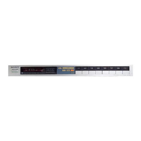
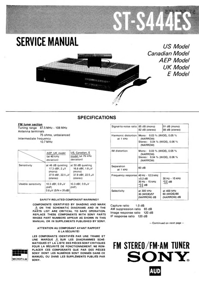
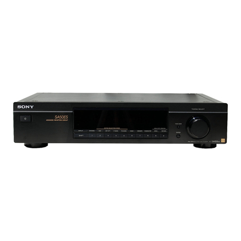
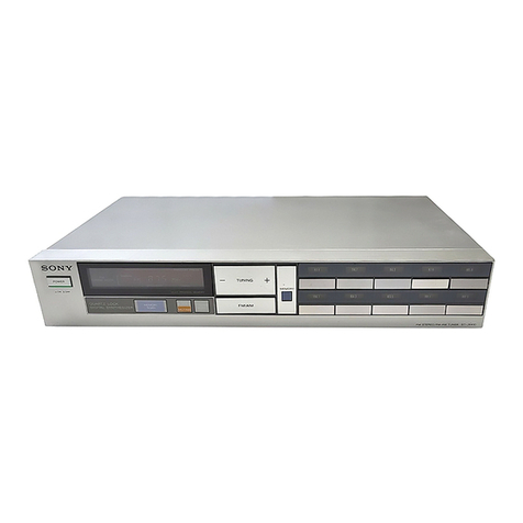
Sony ST-EX880 User manual

MICROFILM
SERVICE MANUAL
FM STEREO/FM-AM TIMER TUNER
AEP Model
UK Model
ST-EX880
E Model
Tourist Model
ST-MS717
SPECIFICATIONS
ST-EX880/MS717
ST-EX880/MS717 are the tuner section
in DHC-EX880MD/MD717. Photo: ST-MS717
w
w
w
.
x
i
a
o
y
u
1
6
3
.
c
o
m
Q
Q
3
7
6
3
1
5
1
5
0
9
9
2
8
9
4
2
9
8
T
E
L
1
3
9
4
2
2
9
6
5
1
3
9
9
2
8
9
4
2
9
8
0
5
1
5
1
3
6
7
3
Q
Q
TEL 13942296513 QQ 376315150 892498299
http://www.xiaoyu163.com

– 2 –
TABLE OF CONTENTS
1. SERVICING NOTES............................................... 2
2. GENERAL ................................................................... 3
3. DISASSEMBLY ......................................................... 5
4. ELECTRICAL ADJUSTMENTS......................... 6
5. DIAGRAMS
5-1. Note for Printed Wiring Boards and
Scehmatic Diagrams ....................................................... 7
5-2. Printed Wiring Board – MAIN Section –
(ST-EX880) ..................................................................... 9
5-3. Printed Wiring Board – MAIN Section –
(ST-MS717) ..................................................................... 11
5-4. Schematic Diagram – MAIN Section (1/2) –................. 13
5-5. Schematic Diagram – MAIN Section (2/2) –................. 15
5-6. Printed Wiring Board – PANEL Section – ..................... 17
5-7. Schematic Diagram – PANEL Section – ........................ 19
5-8. Schematic Diagram – RDS Section – (ST-EX880)........ 21
5-9. Printed Wiring Board – RDS Section – (ST-EX880) ..... 21
5-10. Schematic Diagram – POWER Section – ...................... 22
5-11. Printed Wiring Boards – POWER Section – .................. 23
5-12. IC Pin Function Description ........................................... 25
6. EXPLODED VIEWS................................................ 29
7. ELECTRICAL PARTS LIST ............................... 31
SAFETY-RELATED COMPONENT WARNING!!
COMPONENTS IDENTIFIED BY MARK !OR DOTTED
LINE WITH MARK !ON THE SCHEMATIC DIAGRAMS
AND IN THE PARTS LIST ARE CRITICAL TO SAFE
OPERATION. REPLACE THESE COMPONENTS WITH
SONY PARTS WHOSE PART NUMBERS APPEAR AS
SHOWN IN THIS MANUAL OR IN SUPPLEMENTS PUB-
LISHED BY SONY.
SECTION 1
SERVICING NOTES
KEYs FLUORESCENT INDICATOR TUBE/LEDs
CHECK MODE (Work a separately)
1. Press [POWER] button.
2. Press two buttons [POWER] and [SLEEP] simultaneously.
3. LEDs are all turned on, the fluorescent indicator tube displays
“KEY/FL/LED”, and the check mode is set.
1All LED indicators light on mode
↓
2All Fluorescent indicator tube light on mode
↓
3ST segment mode
↓
4RDS segment mode
↓
5Encoder and key check mode
Note:
1) All LED light on mode is kept, when buttons which is pressed to
enter all LED light on mode, release same time.
When release them separate timing, it is moved to next All Fluores-
cent indicator tube light on mode.
2) After all LED light on mode, light on point remove one by one, when
any button pressed or [MULTICONTROLLER] knob turned.
3) Under KEY check mode, every time buttons pressed numerical value
of “KEY=” in FL tube increase.
And that time, numerical value of “ECDR=” increase when
[MULTICONTROLLER] button turn to + direction, and it decrease
turn to – direction.
To exit from this mode, disconnect the power cord.
TUNER CHECK MODE (Work a separately)
1. Press [POWER] button.
2. Press two buttons [POWER] and[ENTER/YES] simultaneously,
and the tuner check mode is set.
3. System power on, set up the tuner function, and test condition
inactive.
Press two buttons [POWER] and [ENTER/YES] simultaneously
to exit, and system power off.
COLD RESET (Work a complex)
The cold reset clears each unit microcomputer memory to initial
conditions.
1. Press [POWER] button to turn the set OFF.
2. Press three buttons [MENU/NO], [PRESET], and [POWER]
simultaneously.
3. A message “COLD SET OK” is displayed on the fluorescent
indicator tube two seconds.
4. Press [POWER] button to turn the set OFF.
5. Remove power cord after the clock is displayed on the fluo-
rescent indicator tube.
6. Connect power cord, press [POWER] button to turn the set
ON, and the set is reset.
4-995-091-1
π
: Hong Kong, Singapore, Malaysia
4-995-091-2
π
: AEP, UK
4-995-091-3
π
:Tourist
MODEL IDENTIFICATION
– Back Panel –
w
w
w
.
x
i
a
o
y
u
1
6
3
.
c
o
m
Q
Q
3
7
6
3
1
5
1
5
0
9
9
2
8
9
4
2
9
8
T
E
L
1
3
9
4
2
2
9
6
5
1
3
9
9
2
8
9
4
2
9
8
0
5
1
5
1
3
6
7
3
Q
Q
TEL 13942296513 QQ 376315150 892498299
http://www.xiaoyu163.com
– 3 –
SECTION 2
GENERAL This section is extracted from
instruction manual.
LOCATION OF CONTROLS
– Front Panel – – Rear Panel –
1I/u(POWER) button
2REMOTE CONTROL receiver
3ONCE, DAILY, REC, SLEEP indicator
4REC button
5DAILY button
6ONCE button
7CLOCK/TIMER SET button
8STEREO/MONO button
9SLEEP button
!º MULTI CONTROLLER knob
!¡ ENTER/YES button
!™ MENU/NO button
!£ BAND button
!¢ RESET button
!∞ Fluorescent indicator tube
!§ AUTO/nbutton
!¶ MANUAL/Nbutton
!• DISPLAY button
!ª TUNER OUT terminal
@º FM/AM ANTENNA terminal
@¡ AU BUS terminal
@™ SYSTEM CONTROL terminal
@£ AC OUTLET (for TA-MS717)
@¢ POWER cord
w
w
w
.
x
i
a
o
y
u
1
6
3
.
c
o
m
Q
Q
3
7
6
3
1
5
1
5
0
9
9
2
8
9
4
2
9
8
T
E
L
1
3
9
4
2
2
9
6
5
1
3
9
9
2
8
9
4
2
9
8
0
5
1
5
1
3
6
7
3
Q
Q
TEL 13942296513 QQ 376315150 892498299
http://www.xiaoyu163.com
– 5 –
MAIN BOARD
Note: Follow the disassembly procedure in the numerical order given.
SECTION 3
DISASSEMBLY
3
case
0
three screws
(BVTP3
×
10)
1
two screws
(case3 TP2)
4
flat type wire (19 core)
(CN102)
!¡
claw
7
two claws
6
two screws
(BVTT3
×
6)
7
claw
8
front panel ass’y
5
connector
(CN104)
!¡
claw
!™
MAIN board
9
two screws
(BVTP3
×
8)
1
two screws
(case3 TP2)
2
screw
(BVTT3
×
6)
w
w
w
.
x
i
a
o
y
u
1
6
3
.
c
o
m
Q
Q
3
7
6
3
1
5
1
5
0
9
9
2
8
9
4
2
9
8
T
E
L
1
3
9
4
2
2
9
6
5
1
3
9
9
2
8
9
4
2
9
8
0
5
1
5
1
3
6
7
3
Q
Q
TEL 13942296513 QQ 376315150 892498299
http://www.xiaoyu163.com

– 6 –
0 dB=1 µV
Note: As a front-end (FE1) is difficult to repair if faulty, replace it with
new one.
AM Section Adjustment
Setting:
AMTuned Level Adjustment
Band: AM or MW
Procedure:
1. Set the output of SSG so that the input level of the set be-
comes 55 dBµ/m.
2. Tune the set to 999 kHz or 1,000 kHz.
3. Adjust RV1 to the point (moment) when the TUNED indica-
tor will change from going off to going on.
Adjustment Location : MAIN board
FM Section Adjustment
Note: This adjustment should be performed after the AM Tuned Level
Adjustment due to the same adjustment element.
Setting:
FMTuned Level Adjustment
Band: FM
Procedure:
1. Supply a 26 dBµ 98 MHz signal from the ANTENNA termi-
nal.
2. Tune the set to 98 MHz.
3. If the TUNED indicator does not light, adjust RV2 to the point
(moment) when the TUNED indicator will change from going
off to going on.
Adjustment Location: MAIN board
SECTION 4
ELECTRICAL ADJUSTMENTS
AM RF SSG
loop antenna
set
loop antenna
(Supplied accessories)
60 cm AM ANTENNA
terminal
30% amplitude
modulation by
400 Hz signal
Carrier frequency: 999 kHz (at 9 k step)
1,000 kHz (at 10 k step)
Output level : 25 dB Field strength dB (
µ
V/m) =SSG output level dB (
µ
V/m) –26 dB.
Carrier frequency: 98 MHz
Modulation : AUDIO 1 kH, 75 kHz
deviation (100%)
Output level : 26 dB
µ
(17.8
µ
V) FM ANTENNA termina
l
(75
Ω
open)
75
Ω
coaxial
set
FM RF stereo signal
generator
RV1
IC1
FE1
RV2
Adjustment Location:
[MAIN BOARD] (Component Side)
w
w
w
.
x
i
a
o
y
u
1
6
3
.
c
o
m
Q
Q
3
7
6
3
1
5
1
5
0
9
9
2
8
9
4
2
9
8
T
E
L
1
3
9
4
2
2
9
6
5
1
3
9
9
2
8
9
4
2
9
8
0
5
1
5
1
3
6
7
3
Q
Q
TEL 13942296513 QQ 376315150 892498299
http://www.xiaoyu163.com
ST-EX880/MS717
– 7 – – 8 –
SECTION 5
DIAGRAMS
5-1. NOTE FOR PRINTED WIRING BOARDS AND SCHEMATIC DIAGRAMS
Note on Schematic Diagram:
• All capacitors are in µF unless otherwise noted. pF: µµF
50 WV or less are not indicated except for electrolytics
and tantalums.
• All resistors are in Ωand 1/4W or less unless otherwise
specified.
•¢: internal component.
•2: nonflammable resistor.
•C: panel designation.
Note on Printed Wiring Boards:
•X: parts extracted from the component side.
•¢: internal component.
• Indication of transistor.
Abbreviation:
HK : Hong Kong
JE :Tourist
MY : Malaysia
SP : Singapore
•U: B+ Line.
•V: B– Line.
•H: adjustment for repair.
• Voltages and waveforms are dc with respect to ground
under no-signal (detuned) conditions.
no mark : FM
( ) : AM (MW)
〈〈 〉〉 : STAND BY
[ ] : MUTING ON
• Voltages aretakenwithaVOM(Input impedance10 MΩ).
Voltage variations may be noted due to normal produc-
tion tolerances.
• Waveforms are taken with a oscilloscope.
Voltage variations may be noted due to normal produc-
tion tolerances.
• Circled numbers refer to waveforms.
• Signal path.
F: FM
f: AM (MW)
Note: The components identified by mark !or dotted line
with mark !are critical for safety.
Replace only with part number specified.
B
These are omitted.
CE
Q
• Circuit Boards Location
• Waveforms
– MAIN Section –
1IC51 1(XIN)
2IC201 $¡ (X2)
3IC201 $¢ (XT2)
2.9Vp-p
4.5 MHz
– PANEL Section –
4IC901 @º (XOUT)
5IC901 @¡ (XIN)
4.4Vp-p
10 MHz
4.8Vp-p
32.768 kHz
5.2Vp-p
513 kHz
880 mVp-p
504 kHz
AC OUTLET board
(Tourist model)
TRANSFORMER board
PANEL board
RDS board
(ST-EX880)
MAIN boar
d
w
w
w
.
x
i
a
o
y
u
1
6
3
.
c
o
m
Q
Q
3
7
6
3
1
5
1
5
0
9
9
2
8
9
4
2
9
8
T
E
L
1
3
9
4
2
2
9
6
5
1
3
9
9
2
8
9
4
2
9
8
0
5
1
5
1
3
6
7
3
Q
Q
TEL 13942296513 QQ 376315150 892498299
http://www.xiaoyu163.com
ST-EX880/MS717
D1 F-1
D2 E-2
D103 G-7
D104 E-7
D105 E-6
D125 B-5
D143 D-6
D161 D-7
D191 D-2
D272 G-8
D281 H-4
D282 G-4
IC1 E-4
IC51 C-2
IC111 C-7
IC171 I-6
IC201 G-6
Q1 C-4
Q2 C-4
Q9 C-4
Q10 C-5
Q11 A-3
Q12 A-4
Q13 A-4
Q14 B-4
Q15 B-4
Q55 E-2
Q121 B-5
Q122 B-5
Q123 C-5
Q141 D-6
Q142 D-6
Q201 F-6
Q202 B-6
Q203 B-7
Q273 G-8
Q274 G-8
Q281 H-4
– 9 – – 10 –
5-2. PRINTED WIRING BOARD – MAIN Section – (ST-EX880)
•See page 7 for Circuit Boards Location.
• Semiconductor
Location
Ref. No. Location
(Page 21)
(Page 20)
(Page 24)
w
w
w
.
x
i
a
o
y
u
1
6
3
.
c
o
m
Q
Q
3
7
6
3
1
5
1
5
0
9
9
2
8
9
4
2
9
8
T
E
L
1
3
9
4
2
2
9
6
5
1
3
9
9
2
8
9
4
2
9
8
0
5
1
5
1
3
6
7
3
Q
Q
TEL 13942296513 QQ 376315150 892498299
http://www.xiaoyu163.com
ST-EX880/MS717
– 11 – – 12 –
5-3. PRINTED WIRING BOARD – MAIN Section – (ST-MS717)
•See page 7 for Circuit Boards Location.
D1 F-1
D2 E-2
D103 G-7
D104 E-7
D105 E-6
D125 B-5
D143 D-6
D161 D-7
D191 D-2
D272 G-8
D281 H-4
D282 G-4
IC1 E-4
IC51 C-2
IC111 C-7
IC171 I-6
IC201 G-6
Q1 C-4
Q2 C-4
Q9 C-4
Q10 C-5
Q55 E-2
Q121 B-5
Q122 B-5
Q123 C-5
Q141 D-6
Q142 D-6
Q201 F-6
Q202 B-6
Q203 B-7
Q273 G-8
Q274 G-8
Q281 H-4
• Semiconductor
Location
Ref. No. Location
(Page 24)
(Page 20)
w
w
w
.
x
i
a
o
y
u
1
6
3
.
c
o
m
Q
Q
3
7
6
3
1
5
1
5
0
9
9
2
8
9
4
2
9
8
T
E
L
1
3
9
4
2
2
9
6
5
1
3
9
9
2
8
9
4
2
9
8
0
5
1
5
1
3
6
7
3
Q
Q
TEL 13942296513 QQ 376315150 892498299
http://www.xiaoyu163.com

ST-EX880/MS717
– 13 – – 14 –
5-4. SCHEMATIC DIAGRAM – MAIN Section (1/2) –
•See page 8 forWaveforms.
The components identified by mark !or dotted
line with mark !are critical for safety.
Replaceonly withpart numberspecified.
(Page 15)
w
w
w
.
x
i
a
o
y
u
1
6
3
.
c
o
m
Q
Q
3
7
6
3
1
5
1
5
0
9
9
2
8
9
4
2
9
8
T
E
L
1
3
9
4
2
2
9
6
5
1
3
9
9
2
8
9
4
2
9
8
0
5
1
5
1
3
6
7
3
Q
Q
TEL 13942296513 QQ 376315150 892498299
http://www.xiaoyu163.com
ST-EX880/MS717
– 15 – – 16 –
5-5. SCHEMATIC DIAGRAM – MAIN Section (2/2) –
•See page 8 forWaveforms.
(Page 21)
(Page 20)
(Page 14)
(Page 22)
w
w
w
.
x
i
a
o
y
u
1
6
3
.
c
o
m
Q
Q
3
7
6
3
1
5
1
5
0
9
9
2
8
9
4
2
9
8
T
E
L
1
3
9
4
2
2
9
6
5
1
3
9
9
2
8
9
4
2
9
8
0
5
1
5
1
3
6
7
3
Q
Q
TEL 13942296513 QQ 376315150 892498299
http://www.xiaoyu163.com
ST-EX880/MS717
– 17 – – 18 –
5-6. PRINTED WIRING BOARD – PANEL Section –
•See page 7 for Circuit Boards Location.
(Page 10, 12)
w
w
w
.
x
i
a
o
y
u
1
6
3
.
c
o
m
Q
Q
3
7
6
3
1
5
1
5
0
9
9
2
8
9
4
2
9
8
T
E
L
1
3
9
4
2
2
9
6
5
1
3
9
9
2
8
9
4
2
9
8
0
5
1
5
1
3
6
7
3
Q
Q
TEL 13942296513 QQ 376315150 892498299
http://www.xiaoyu163.com
ST-EX880/MS717
– 21 – – 22 –
5-8. SCHEMATIC DIAGRAM – RDS Section – (ST-EX880)
5-9. PRINTED WIRING BOARD – RDS Section – (ST-EX880)
•See page 7 for Circuit Boards Location.
5-10. SCHEMATIC DIAGRAM – POWER Section –
The components identified by mark !or dotted
line with mark !are critical for safety.
Replaceonly withpart numberspecified.
(Page 15)
(Page 9)
(Page 15)
w
w
w
.
x
i
a
o
y
u
1
6
3
.
c
o
m
Q
Q
3
7
6
3
1
5
1
5
0
9
9
2
8
9
4
2
9
8
T
E
L
1
3
9
4
2
2
9
6
5
1
3
9
9
2
8
9
4
2
9
8
0
5
1
5
1
3
6
7
3
Q
Q
TEL 13942296513 QQ 376315150 892498299
http://www.xiaoyu163.com
ST-EX880/MS717
– 23 – – 24 –
5-11. PRINTED WIRING BOARDS – POWER Section –
•See page 7 for Circuit Boards Location.
(Page 10, 12)
w
w
w
.
x
i
a
o
y
u
1
6
3
.
c
o
m
Q
Q
3
7
6
3
1
5
1
5
0
9
9
2
8
9
4
2
9
8
T
E
L
1
3
9
4
2
2
9
6
5
1
3
9
9
2
8
9
4
2
9
8
0
5
1
5
1
3
6
7
3
Q
Q
TEL 13942296513 QQ 376315150 892498299
http://www.xiaoyu163.com
ST-EX880/MS717
– 25 – – 26 –
5-12. IC PIN FUNCTION DESCRIPTION
•MAIN BOARD IC201 µPD78016FGC-544-AB8 (SYSTEM CONTROLLER)
Pin No. Pin Name I/O Function
1 to 4 DATA 0 to
DATA 3 I/O Two-way data bus with the system control bus
5 IF+50 I Fixed at “L” in this set
6 IF–50 O Fixed at “L” in this set
7, 8 GND — Ground terminal
9 VSS — Ground terminal
10 POWER O Power on/off control signal output for the +10V and +5V power supply
“L”: power on, “H”: standby
11 MUTE O Tuner muting on/off control signal output terminal “L”: muting on
12 AC RELAY O Relay drive signal output for the AC on/off control “L”: standby, “H”: power on
13, 14 NC O Not used (open)
15 AM MONO O AM forced monaural control signal output terminal “H”: forced monaural Not used (open)
16 AM/FM O FM/AM selection signal output terminal Not used (open)
17 IFNG O Intermediate frequency count effect signal output terminal “L”: NG, “H”: OK
Not used (open)
18 STEREO I Stereo detection signal input from the LA1835 (IC1) “L”: stereo
19 SIGNAL I FM/AM frequency detection signal input from the LA1835 (IC1) “L”: tuned, “H”: detuned
20 DATA IN I PLL serial data input from the FM/AM PLL (IC51)
21 DATA OUT O PLL serial data output to the FM/AM PLL (IC51)
22 CLOCK O PLL serial data transfer clock signal output to the FM/AM PLL (IC51)
23 CE O PLL serial chip enable signal output to the FM/AM PLL (IC51)
24 VSS — Ground terminal
25 SIRCS IN I Sircs remote control signal input from the remote control receiver (IC902)
26 STAND BY O LED drive signal output for the STANDBY indicator Not used (open)
27 ONCE O LED drive signal output for the ONCE indicator (D905) “L”: LED on
28 DAILY O LED drive signal output for the DAILY indicator (D904) “L”: LED on
29 REC O LED drive signal output for the REC indicator (D903) “L”: LED on
30 SLEEP O LED drive signal output for the SLEEP indicator (D902) “L”: LED on
31
ENCORDER IN A
IJog dial pulse (A) input from the rotary encoder (S915) (for MULTI CONTROLLER)
32
ENCORDER IN B
IJog dial pulse (B) input from the rotary encoder (S915) (for MULTI CONTROLLER)
33 AUBUS IN I Sircs remote control signal input for the audio bus
34 AUBUS OUT O Sircs remote control signal output for the audio bus
35 RESET I System reset signal input from the reset signal generator circuit “L”: reset
For several hundreds msec. after the power supply rises, “L” is input, then it changes to “H”
36 RDS CLK I Serial data transfer clock signal input from the RDS decoder (IC302)
Used for the ST-EX880 (ST-MS717: fixed at “L”)
37 CLOCK I/O Bus data transfer/reading clock signal in/out terminal for the system control bus
38 BUSY I/O Busy signal in/out terminal for the system control bus
39 AC OFF I AC off detection signal input terminal “L”: AC off
40 VDD — Power supply terminal (+5V)
41 X2 O Main system clock output terminal (10 MHz)
42 X1 I Main system clock input terminal (10 MHz)
43 GND IC (VPP) — Ground terminal
44 XT2 O Sub system clock output terminal (32.768 kHz)
45 XT1 I Sub system clock input terminal (32.768 kHz)
46 AVSS — Ground terminal (for A/D converter)
Pin No. Pin Name I/O Function
47 KEY IN 1 I Key input terminal (A/D input) (S907 to S913)
ONCE, DAILY, REC, SLEEP, CLOCK/TIMER SET, ENTER/YES, MENU/NO keys input
48 KEY IN 2 I Key input terminal (A/D input) (S901 to S906)
STEREO/MONO, BAND, PRESET, MANUAL, AUTO, DISPLAY keys input
49 KEY IN 3 I Key input terminal (A/D input) (S914) I/u(power) key input
50 RDS DATA I Serial data input from the RDS decoder (IC302)
Used for the ST-EX880 (ST-MS717: fixed at “L”)
51 DESTINATION I Input terminal for the destination setting
(Tourist model: fixed at “L”, Except Tourist model: open)
52 DESTINATION I Input terminal for the destination setting (fixed at “L”)
53 DESTINATION I Input terminal for the destination setting
(Tourist model: open, Except Tourist model: fixed at “L”)
54 DESTINATION I Input terminal for the destination setting (ST-EX880: open, ST-MS717: fixed at “L”)
55 AVDD — Power supply terminal (+5V) (for A/D converter)
56 AVREF I Reference voltage (+5V) input terminal (for A/D converter)
57 GND — Ground terminal
58 SDATA O Serial data output to the fluorescent indicator tube driver (IC901)
59 SCK O Serial data transfer clock signal output to the fluorescent indicator tube driver (IC901)
60 CS O Chip select signal output to the fluorescent indicator tube driver (IC901) “L” active
61 RESET O Reset signal output to the fluorescent indicator tube driver (IC901) “L”: reset
62 ERRORS O Output terminal of the error monitor Not used (open)
63 CORRECTION O Output terminal of the correction monitor Not used (open)
64 RECEIVED O Output terminal of the receive monitor Not used (open)
w
w
w
.
x
i
a
o
y
u
1
6
3
.
c
o
m
Q
Q
3
7
6
3
1
5
1
5
0
9
9
2
8
9
4
2
9
8
T
E
L
1
3
9
4
2
2
9
6
5
1
3
9
9
2
8
9
4
2
9
8
0
5
1
5
1
3
6
7
3
Q
Q
TEL 13942296513 QQ 376315150 892498299
http://www.xiaoyu163.com
– 27 –
• IC Block Diagrams
– MAIN Board –
IC1 LA1835
IC51 LC72130
ALC
BUFF
AM
OSC AM
MIX AM
RF. AMP
AGC
S METER
LEVEL
DET
FM
IF AM
DET
S-CURVE
AM/FM
IF
BUFF
REG
TUNING
DRIVE
COMP
GND
AM/FM
SW
VCC
PHASE
DET
PILOT
DET
VCO
FF
STEREO
DRIVE TRIG
STEREO
SW
MUTE
FF FF
FM
IF FM
DET
DECODER
ANTI BIRDIE
12 3 45 6 7 8 9 10
20 19 18 17 16
1514131211
21222324252627282930
FM-SD
AM-OSC
FM-AFC
AM-RF-IN
AGC
AM. CUT
AM/FM
VCO
MPX-IN
OUT R
OUT L
AMP-IN R
AMP-IN L
R
L
VCO-STOP
ST-LED
AM/FM
AM. SD
AM. SD
IF-BUFF
VCC
DET
FM-IN
AM-MIX
IF
REG
AM-IF
GND
TU-LED
FM
AM
PHASE DETECTOR
CHARGE PUMP
SWALLOW COUNTER
1/16, 1/17 4BITS
12BITS PROGRAMMABLE
DRIVER
UNIVERSAL
COUNTER
REFERENCE
DIVIDER
POWER
ON
RESET 1/2
C
2
B
I/F
12 3 45 6 7 8 9 10
20 19 18 17 16 15 14 13
1211
21222324
XOUT
VSS
AOUT2
AIN2
PD2
PD1
AIN1
AOUT1
VDD
FMIN
AMIN
IO2
XIN
D0
CL
D1
CE
BO5
BO1
BO2
BO3
BO4
IO1
IFIN
UNLOCK
DETECTOR
DATA SHIFT REGISTER LATCH
w
w
w
.
x
i
a
o
y
u
1
6
3
.
c
o
m
Q
Q
3
7
6
3
1
5
1
5
0
9
9
2
8
9
4
2
9
8
T
E
L
1
3
9
4
2
2
9
6
5
1
3
9
9
2
8
9
4
2
9
8
0
5
1
5
1
3
6
7
3
Q
Q
TEL 13942296513 QQ 376315150 892498299
http://www.xiaoyu163.com

– 28 –
– RDS Board –
IC302 SAA6579 (ST-EX880 ONLY)
– PANEL Board –
IC901 M66004M6FP
QUALITY BIT
GENERATOR
DEFFERENTIAL
DECODER
BIPHASE
SYMBOL
DECODER
OSCILLATOR
AND
DIVIDER
57kHz
BANDPASS
(8th ORDER)
CONTAS LOOP
VARIABLE AND
FIXED DIVIDER
REFERENCE
VOLTAGE
ANTI-
ALIASING
FILTER
CLOCKED
COMPARATOR
TEST LOGIC AND OUTPUT
SELECTOR SWITCH
RECONSTRUCTION
FILTER
141516 13 12 11 10 9
321 4 5 6 7 8
CLOCK REGENERATION
AND SYNC
VP1
RDCL
TS7
OSCO
OSCI
V
DDD
V
SSD
TEST
TSTL
D
QUAL
RDDA
Vref
MUX
V
DDA
V
SSA
CIN
SCOUT
SEGMENT
OUTPUT
CIRCUIT
(35BIT x 16)
DECODER
INDICATION
CODE
RESISTOR
(8BIT x 16)
DECODER
(35BIT x 16)
CODE/COMMAND
CONTROL
CIRCUIT
INDICATION
CONTROL
RESISTOR
INDICATION
CONTROLLER
DIGIT OUTPUT
CIRCUIT CODE
WRITE
CODE SELECT
SERIAL
RECEIVE
CIRCUIT
OUTPUT
PORT
(2BIT)
CLOCK
GENERATOR
CIRCUIT
RAM
WRITE
2120
19 22
13 32
60
64 - 61 59 - 33
23 - 31
1 - 12 17 • 18
14 • 15 • 16
G13
|
G16
V
CC
2
P1
|
P27
V
SS
XIN
XOUT
V
CC
1
RST
G12
|
G1
VP
CS
SCK
SDATA
P36
|
P28
w
w
w
.
x
i
a
o
y
u
1
6
3
.
c
o
m
Q
Q
3
7
6
3
1
5
1
5
0
9
9
2
8
9
4
2
9
8
T
E
L
1
3
9
4
2
2
9
6
5
1
3
9
9
2
8
9
4
2
9
8
0
5
1
5
1
3
6
7
3
Q
Q
TEL 13942296513 QQ 376315150 892498299
http://www.xiaoyu163.com

– 29 –
SECTION 6
EXPLODED VIEWS
The components identified by
mark !or dotted line with mark
!are critical for safety.
Replace only with part number
specified.
• Items marked “*” are not stocked since they
are seldom required for routine service. Some
delay should be anticipated when ordering
these items.
• The mechanical parts with no reference num-
ber in the exploded views are not supplied.
• Hardware (# mark) list is given in the last of
the electrical parts list.
NOTE:
• -XX and -X mean standardized parts, so they
may have some difference from the original
one.
• Color Indication of Appearance Parts
Example:
KNOB, BALANCE (WHITE) . . . (RED)
↑↑
Parts Color Cabinet's Color
• Abbreviation
HK: Hong Kong MY: Malaysia
JE : Tourist SP : Singapore
Ref. No. Part No. Description Remark Ref. No. Part No. Description Remark
(1) CASE, FRONT PANEL SECTION
6
67
#2
3
8
4
5
1
210
#2
9
1 4-995-074-01 KNOB (JOG)
2 4-988-161-01 SPRING, RING
3 X-4949-861-1 PANEL ASSY, FRONT (ST-EX880)
3 X-4949-873-1 PANEL ASSY, FRONT (ST-MS717)
*4 A-4407-398-A PANEL BOARD, COMPLETE (JE)
*4 A-4407-880-A PANEL BOARD, COMPLETE (AEP, UK)
*4 A-4407-884-A PANEL BOARD, COMPLETE (MY, SP, HK)
5 1-773-110-11 WIRE (FLAT TYPE) (19 CORE)
6 3-363-099-01 SCREW (CASE 3 TP2)
*7 4-900-196-11 CASE
8 4-951-620-01 SCREW (2.6X8), +BVTP
9 4-962-708-01 EMBLEM (4-A), SONY
10 4-995-083-21 PLATE (ST), ORNAMENTAL (ST-EX880)
10 4-995-083-31 PLATE (ST), ORNAMENTAL (ST-MS717)
w
w
w
.
x
i
a
o
y
u
1
6
3
.
c
o
m
Q
Q
3
7
6
3
1
5
1
5
0
9
9
2
8
9
4
2
9
8
T
E
L
1
3
9
4
2
2
9
6
5
1
3
9
9
2
8
9
4
2
9
8
0
5
1
5
1
3
6
7
3
Q
Q
TEL 13942296513 QQ 376315150 892498299
http://www.xiaoyu163.com

– 30 –
Ref. No. Part No. Description Remark Ref. No. Part No. Description Remark
(2) CHASSIS SECTION
51
52
53
56
55
#3
T701
54
#1
#2
not supplied
57
#1
#2
60
AEP, UK
AEP, UK, MY, SP,
HK JE
58
CN951
AEP, MY,SP,
HK MY, SP UK HK JE
59
61
59
61
59
61
62
UK, HK
AEP, MY, SP, JE
51 X-4949-526-1 FOOT (F) ASSY
52 3-703-244-00 BUSHING (2104), CORD
*53 4-949-235-01 HOOK (AEP, MY, SP, JE)
*54 4-995-091-11 PANEL (ST), BACK (MY, SP, HK)
*54 4-995-091-21 PANEL (ST), BACK (ST-EX880)
*54 4-995-091-31 PANEL (ST), BACK (JE)
*55 A-4407-399-A MAIN BOARD, COMPLETE (MY, SP, HK)
*55 A-4407-876-A MAIN BOARD, COMPLETE (AEP, UK)
*55 A-4407-885-A MAIN BOARD, COMPLETE (JE)
56 4-965-822-01 FOOT
*57 1-667-607-11 TRANSFORMER BOARD
*58 1-667-608-11 AC OUTLET BOARD (JE)
!59 1-558-943-41 CORD, POWER (JE)
!59 1-575-651-21 CORD, POWER (AEP, MY, SP, HK)
!59 1-696-571-11 CORD, POWER (UK)
*60 A-4407-877-A RDS BOARD, COMPLETE (AEP, UK)
!61 1-569-007-11 ADAPTOR, CONVERSION 2P (JE)
!61 1-569-008-11 ADAPTOR, CONVERSION 2P (MY, SP)
!61 1-770-019-11 ADAPTOR, CONVERSION PLUG 3P (HK)
62 4-956-370-12 BAND, PLUG FIXED (UK, HK)
!CN951 1-526-794-11 OUTLET, AC (EXCEPT JE)
!T701 1-431-833-11 TRANSFORMER, POWER (ST-EX880)
!T701 1-431-834-11 TRANSFORMER, POWER (ST-MS717)
The components identified by mark !or dotted
line with mark !are critical for safety.
Replace only with part number specified.
w
w
w
.
x
i
a
o
y
u
1
6
3
.
c
o
m
Q
Q
3
7
6
3
1
5
1
5
0
9
9
2
8
9
4
2
9
8
T
E
L
1
3
9
4
2
2
9
6
5
1
3
9
9
2
8
9
4
2
9
8
0
5
1
5
1
3
6
7
3
Q
Q
TEL 13942296513 QQ 376315150 892498299
http://www.xiaoyu163.com
This manual suits for next models
1
Table of contents
Other Sony Tuner manuals

Sony
Sony FD-525 User manual

Sony
Sony STR-NX1 User manual

Sony
Sony WRR-850A User manual

Sony
Sony WRU-806B User manual

Sony
Sony ST-S3000ES User manual

Sony
Sony WRR-861B Installation and operation manual

Sony
Sony MB-8N Installation and operation manual

Sony
Sony WRR-801A User manual

Sony
Sony ST-JX401 User manual

Sony
Sony WRR-855B User manual

Sony
Sony WRR-862A User manual

Sony
Sony WRU-801A User manual

Sony
Sony ST-JX661 User manual

Sony
Sony Ipela NSR-S10 User manual

Sony
Sony hmd-m11 User manual

Sony
Sony URX-S03D User manual

Sony
Sony Dream Machine ICF-C743 User manual
Sony
Sony WRR-800A User manual

Sony
Sony WRR-805A User manual

Sony
Sony ST-J88B User manual