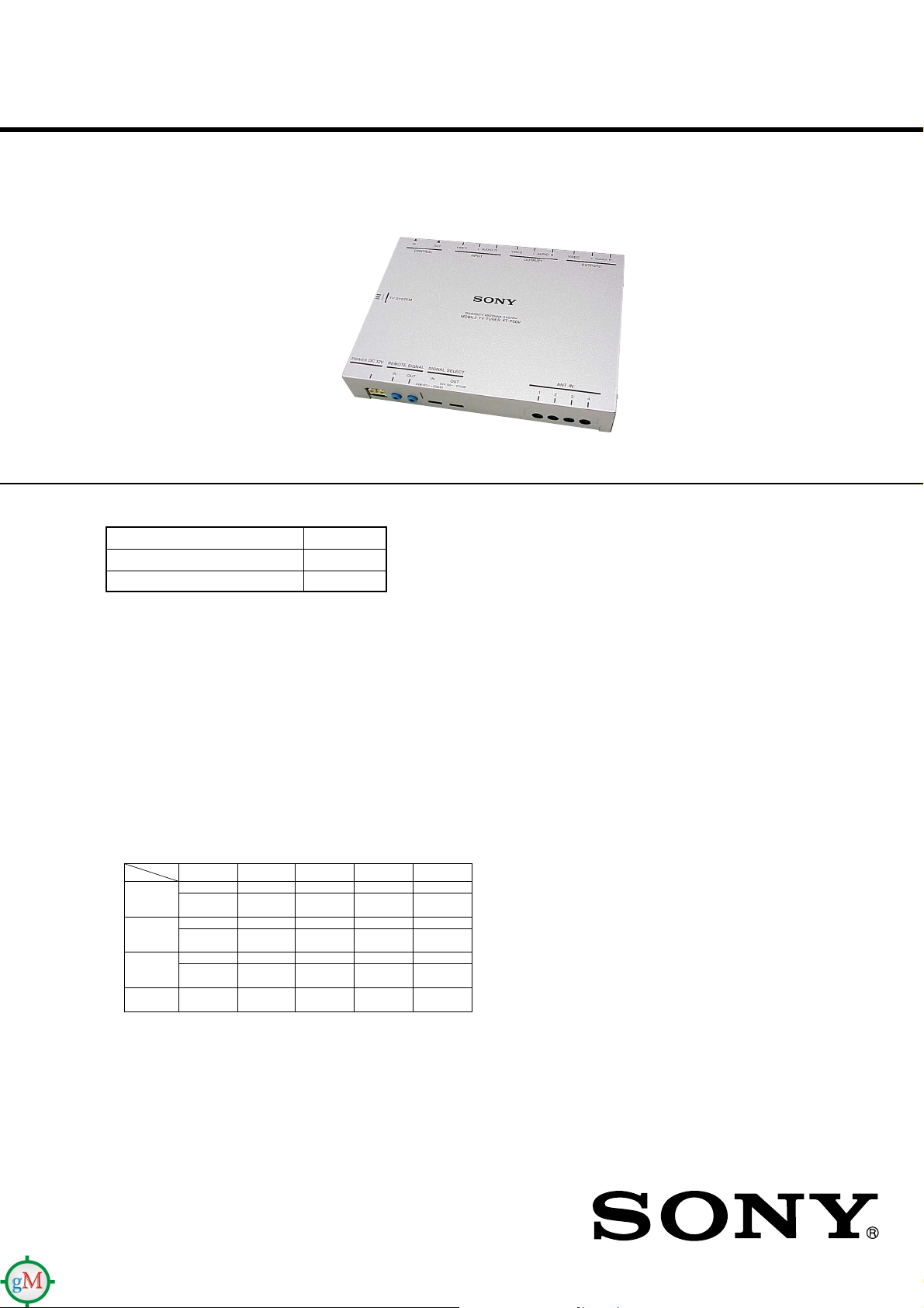
Sony XT-P50V User manual

SERVICE MANUAL
MOBILE TV TUNER
AEP Model
UK Model
E Model
Australian Model
Chinese Model
XT-P50V
Ver 1.0 2002.09
9-874-168-01 Sony Corporation
2002I0500-1 e Vehicle Company
C2002.09 Published by Sony Engineering Corporation
SPECIFICATIONS
The XT-P50V is composed of the following models.
TV tuner unit XT-P50V
TV Antenna VCA-116
Wireless Remote Commander RM-X124
Tuner unit
Reception format PAL
Power requirements 12 V DC, from car battery
(negative ground)
Power consumption Approx. 0.5 A
Inputs Video/audio (Sony BUS compatible)(1)
Sony BUS (1)
TV aerial (4)
Outputs Video/audio (Sony BUS compatible)(2)
Sony BUS (1)
Dimensions Approx. 185.5 ×31 ×137 mm
(W ×H ×D)
Mass Approx. 0.7 kg
Channel coverage
Wireless remote commander RM-X124
Power requirements CR2025 lithium battery
Operable range Approx. 2.5 m
Dimension 50 ×86 ×11.5 mm (W ×H ×D)
Mass Approx. 36 g (including a battery)
Design and specifications are subject to change without notice.
AUSTRALIA
VHF LOW
VHF HIGH
UHF
IF VIDEO
IF AUDIO
0 - 4
CH
5 - 12
CH
28 - 69
CH
38.90
MHz
33.40
MHz
CCIR
2 - 4
CH
5 -12
CH
21 - 69
CH
38.90
MHz
33.40
MHz
48.25
MHz
-
62.25
MHz
175.25
MHz
-
224.25
MHz
471.25
MHz
-
855.25
MHz
UK
–
–
–
–
21 - 69
CH
38.90
MHz
32.90
MHz
471.25
MHz
-
855.25
MHz
CHINA
1 - 5
CH
6 - 12
CH
13 - 57
CH
38.90
MHz
32.40
MHz
49.75
MHz
-
85.25
MHz
168.25
MHz
-
216.25
MHz
471.25
MHz
-
863.25
MHz
ITALY
A - C
CH
D - H2
CH
21 - 69
CH
38.90
MHz
33.40
MHz
53.75
MHz
-
82.25
MHz
175.25
MHz
-
224.25
MHz
471.25
MHz
-
855.25
MHz
46.25
MHz
-
95.25
MHz
102.25
MHz
-
224.25
MHz
527.25
MHz
-
814.25
MHz

2
XT-P50V
TABLE OF CONTENTS
1. GENERAL ................................................................... 2
2. TEST MODE.............................................................. 5
3. ELECTRICAL ADJUSTMENTS......................... 5
4. DIAGRAMS
4-1. Block Diagram –AUDIO Section – ............................... 7
4-2. Block Diagram –VIDEO Section – ............................... 8
4-3. Block Diagram
–BUS CONTROL/POWER SUPPLY Section – ............ 9
4-4. Note for Printed Wiring Board and
Schematic Diagrams ....................................................... 10
4-5. Schematic Diagram –HIDEAWAY Board (1/3) – ......... 11
4-6. Schematic Diagram –HIDEAWAY Board (2/3) – ......... 12
4-7. Schematic Diagram –HIDEAWAY Board (3/3) – ......... 13
4-8. Printed Wiring Board
–HIDEAWAY Board (Component Side) – ..................... 14
4-9. Printed Wiring Board
–HIDEAWAY Board (Conductor Side) – ....................... 15
4-10. IC Pin Function Description ........................................... 18
5. EXPLODED VIEW................................................... 20
6. ELECTRICAL PARTS LIST ............................... 21
Notes on chip component replacement
•Never reuse a disconnected chip component.
•Notice that the minus side of a tantalum capacitor may be dam-
aged by heat.
SECTION 1
GENERAL
This section is extracted from
instruction manual.
ANT IN
POWER
DC 12V
OUTPUT
REMOTE
SIGNAL OUT
REMOTE
SIGNAL IN
3
2
DISC
SEEK
SOURCE MODE ATT
OFF
OPEN/
CLOSE
.>
VOL
CONTROL OUT OUTPUT
INPUT
CONTROL IN
Black
Schwarz
XT-P50V
To the +12 V power terminal
which is energized in the
accessory position of the
ignition key switch
an den +12-V-
Stromversorgungsanschluss, an
dem Spannung anliegt, wenn
sich der Zündschlüssel in der
Zubehörposition befindet
To the +12 V power terminal
which is energized at all times
an den +12-V-
Stromversorgungsanschluss, an
dem immer Spannung anliegt
To a metal surface of the car
an eine Metalloberfläche des
Wagens
TV aerial 6
Fernsehantenne 6
Yellow
Gelb Filter + fuse (5 A)
Filter + Sicherung (5 A)
Power supply leads 1(5.5 m)
Stromversorgungskabel 1(5,5 m)
Red
Rot
Fuse (0.5 A)
Sicherung
(0,5 A)
Connection box XA-114
(supplied with XAV-7W)
Anschlussdose XA-114
(mit XAV-7W mitgeliefert)
CD/ MD changer,
or Source selector XA-C30
CD/MD-Wechsler oder
Signalquellenwähler XA-C30
Media Center main unit
XAV-7W
Mediencenter-Hauptgerät
XAV-7W
TV tuner unit
Fernsehtuner
XT-P50V
TV tuner unit
Fernsehtuner
XT-P50V
1
2
Connection box XA-117
(supplied with XVM-R75)
Anschlussdose XA-117
(mit XVM-R75 mitgeliefert)
Overhead monitor
XVM-R75
Deckenmonitor
XVM-R75
DVD changer
DVX-100
DVD-Wechsler
DVX-100
Blue
Blau
6 m
6 m
To the power remote cord (blue)
of the monitor*
(when connected to the monitor)
*If the Sony BUS connection is
used, this connection is not
necessary.
an Stromversorgungskabel (blau)
eines Monitors*
(bei Anschluss an einen Monitor)
*Bei einer Sony-BUS-Verbindung
ist diese Verbindung nicht
erforderlich.

3
XT-P50V
7
1
2
3
8
12
Long
Lang
Leave clearance of at least 50 mm.
Mindestens 50 mm Abstand lassen.
Inside of rear window
Innenseite der Heckscheibe
Secure with tape under seat.
Mit Klebeband unter dem Sitz befestigen.
TV tuner unit
XT-P50V
Fernsehtuner
XT-P50V
90°90°
Do not bend sharply.
Nicht scharf knicken.
Bend in a smooth curve.
In einer Rundung biegen.
Leave clearance of at least 50 mm.
Mindestens 50 mm Abstand lassen. Short
Kurz
Insert between
metal plates.
Zwischen
Metallplatten
einsetzen.
Slide terminal cover forward to
remove.
Anschlussabdeckung zum Abnehmen
nach vorne schieben.
Screw
Schraube
Terminal cover
Anschlussabdeckung
Support clamper 8
Halteklemme 8
Ground plate 7
Masseplatte 7
Bring into contact with metal surface of the car.
Mit Metalloberfläche des Fahrzeugs in Berührung
bringen.
Attach while adjusting angle and
position.
Anbringen, dabei Winkel und Position
einstellen. Fix support clamper in center of aerial rod.
Halteklemme in der Mitte des Antennenstabs
anbringen.
RLV
1
2
REMOTE
COMMANDER
SIGNAL OUT
REMOTE
SIGNAL IN REMOTE
SIGNAL OUT
SIGNAL SELECT
OUT
DVX-100 OTHERS
IN
XVM-R75 OTHERS
OUTPUT
INPUT
CONTROL
OUT
CONTROL
INPUT
DISC
SEEK
SOURCE MODE ATT
OFF
OPEN/
CLOSE
.>
VOL
TV SYSTEM
1
2
3
4
Bus cable 2(5.3 m)
Buskabel 2(5,3 m)
RCA interconnects 3(5.3 m)
Cinch-Verbindungen 3(5,3 m)
*
Connection box
XA-114
(supplied with XAV-7W)
Anschlussdose
XA-114
(mit XAV-7W mitgeliefert)
1
2
XT-P50V
*
DVD changer
DVX-100
DVD-Wechsler
DVX-100
*
Connection box XA-117
(supplied with XVM-R75)
Anschlussdose XA-117
(mit XVM-R75 mitgeliefert)
RCA interconnects 3(5.3 m)
Cinch-Verbindungen 3(5,3 m)
XT-P50V
*
Stereo mini plug-to-plug
cable 4(5 m)
Kabel mit
Stereoministecker-Stecker
4(5 m)
*
Media Center main unit
XAV-7W
Mediencenter-Hauptgerät
XAV-7W
TV SYSTEM switch
Schalter TV SYSTEM
*
Monitor
Monitor
SIGNAL SELECT switch
Schalter SIGNAL SELECT
*
option
Option
*
RCA interconnects
Cinch-Verbindungen * (5 m)
6
Inside of rear window
Innenseite der Heckscheibe
Inside of rear window
Innenseite der Heckscheibe
Peel off lining here.
Verkleidung hier ablösen.
5
Hook-and-loop fastener 5
Haken- und Ösenverschluss 5
On installation surface
Auf Montageoberfläche
Hook-and-loop fastener 5
Haken- und Ösenverschluss 5
XT-P50V

4
XT-P50V
Precautions
•This unit is designed for negative ground 12 V DC systems
only.
•Do not get the wires under a screw, or caught in moving parts
(e.g. seat railing).
•Before making connections, turn the car ignition off to avoid
short circuits.
•Connect the yellow and red power input leads only after all
other leads have been connected.
•Run all ground wires to a common ground point.
•Be sure to insulate any loose unconnected wires with electrical
tape for safety.
Notes on the power supply cord (yellow)
•When connecting this unit in combination with other stereo
components, the connected car circuit’s rating must be higher than
the sum of each component’s fuse.
•When no car circuits are rated high enough, connect the unit
directly to the battery.
Fuse replacement
When replacing the fuse, be sure to use one matching the
amperage rating stated on the original fuse. If the fuse blows,
check the power connection and replace the fuse. If the fuse
blows again after replacement, there may be an internal
malfunction. In such a case, consult your nearest Sony dealer.
Parts list (1)
•The numbers in the list are keyed to those in the instructions.
• Use 9and 0to organize cords.
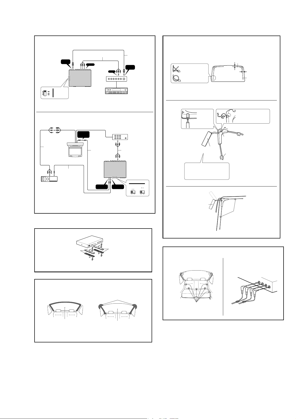
Connection example (2)
The XAV-7W is shown for the Sony BUS connection and the
XVM-R75 is shown for the other connection in this operating
instructions.
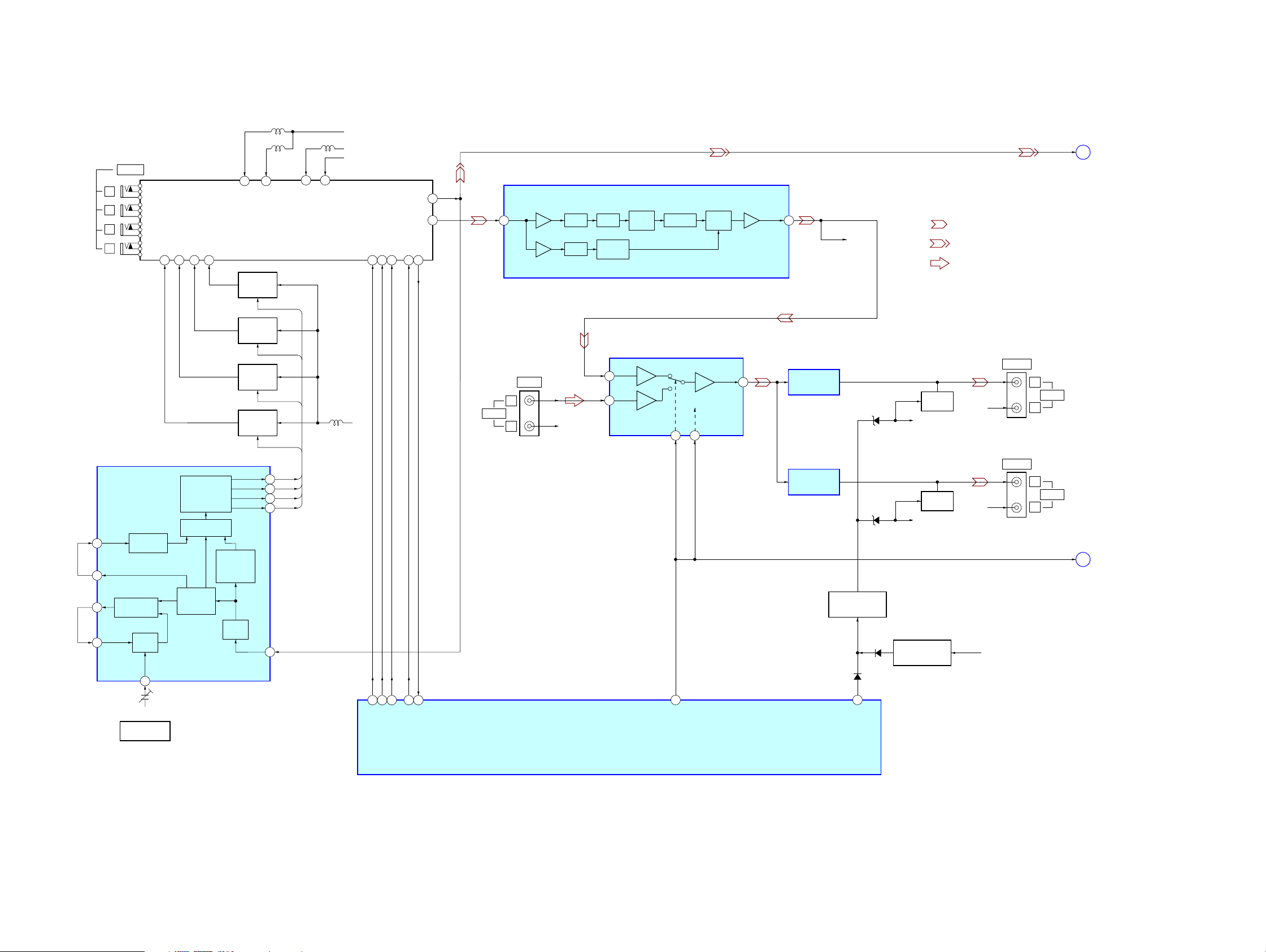
Power connection diagram (3)
Sony BUS connection diagram
(4-1)
When making the Sony BUS connection, the connected Media
Center (ex: XAV-7W) is only controllable with the wireless
remote commander supplied with the Media Center.
After connection
Set the TV SYSTEM selector on the side of the tuner unit, to
the correct position for your area.
Be sure to reset the connected Media Center main unit after
setting the TV system.
Position Area
1The United Kingdom
2Europe and Italy
3China and Hong Kong
IR connection diagram (4-2)
•Be sure to set the SIGNAL SELECT switch on the tuner unit
according to the connected equipment, or the wireless remote
commander does not respond.
•The Sony BUS connection takes priority over the IR
connection.
SIGNAL SELECT OUT switch
Set the switch to “DVX-100” when DVX-100 is connected, and
set to “OTHERS” when other equipment is connected.
SIGNAL SELECT IN switch
Set to “XVM-R75” when XVM-R75 is connected, and set to
“OTHERS” when other equipment is connected.
Fuse (5 A)
5
Fuse (0.5 A)
Power supply lead (3-)Aerial cord (3-)
Before installation
•Install the aerials only on the rear window.
•Keep the aerials away from other aerials on the car, such as
for CB or amateur radio, cell phone, etc. If installed too close,
aerials may cause mutual interference.
•On days of high humidity (rain, fog, etc.), make sure that the
installation surface is fully dry before beginning the
installation. Wet conditions will reduce the adhesive strength
and may cause the aerials to fall off.
•If the installation surface is cold, warm it up first with the car
heater, rear window defogger, a hair dryer or similar. This
will increase adhesive strength.
Installing the TV tuner unit (5)
Notes
•Ensure that the mounting surface is clean.
•Do not install the TV tuner unit
–in locations subject to high temperatures.
–in locations subject to direct sunlight, warm air from heater
outlets, or other locations that can get hot.
•When attaching the hook-and-loop fastener to the bottom of the
TV tuner unit, do not cover the model name plate in the center.
Keep the units and connection cables apart.
The Media Center main unit, the monitor, TV tuner unit, and RCA
interconnects should not be in close proximity. Otherwise noise
interference may affect the TV picture.
Installing the TV aerials (6)
Select a fairly flat section of the rear window for installation. If
the glass is strongly curved, the aerial may come loose. Wipe
the intended installation area with a dry cloth to remove any
moisture or dust.
In cars which have a lining (pillar) near the rear window,
remove the lining to gain access to the metal for use as ground.
It is not necessary to scratch off the paint from the metal
surface.
Checking the mounting position for
TV aerials (7-1)
Verify the left and right aerial positions. Pull the aerial rods
straight out, and provisionally fasten them with tape or similar.
Take care that the rods from the left and right aerials do not
overlap or touch each other.
In some cars, it may not be possible to extend the long rod fully.
In such a case, bend the rod in a smooth curve.
Notes
•When installing the aerials, try to avoid the defogger wiring.
•Do not touch the adhesive surface or reposition the aerial, as this
will decrease adhesive strength.
•The short aerial rod should be on top. If the long rod is on top,
sufficient sensitivity may not be achieved.
Attaching ground plate to aerials
body (7-2)
Be sure to mount the ground plate 7. Otherwise aerial
sensitivity will be reduced.
At this stage, the support clamper should only be snapped onto
the aerial but not yet glued in place.
After installation
•For 24 hours after installation, do not subject the aerials to
rain, splashes of water, or strong force.
•Before starting to drive, make sure that the aerials are securely
fastened.
•Also after starting to use the system, check the aerials from
time to time.
•Do not wipe the aerial body, rods, or cables with alcohol,
benzine, solvents, gasoline, wax, or similar, as this can cause
deformation or other damage.
•Reception may be impaired in the following locations:
–Between tall buildings
–In the vicinity of high voltage power lines
–Inthe vicinity of flying aircraft
–In the vicinity of electric trains and streetcars
–In mountainous areas or areas far removed from broadcast
transmitters
–In tunnels
–Very close to commercial, amateur radio transmitters or
Sony TV tuner unit XT-P50V
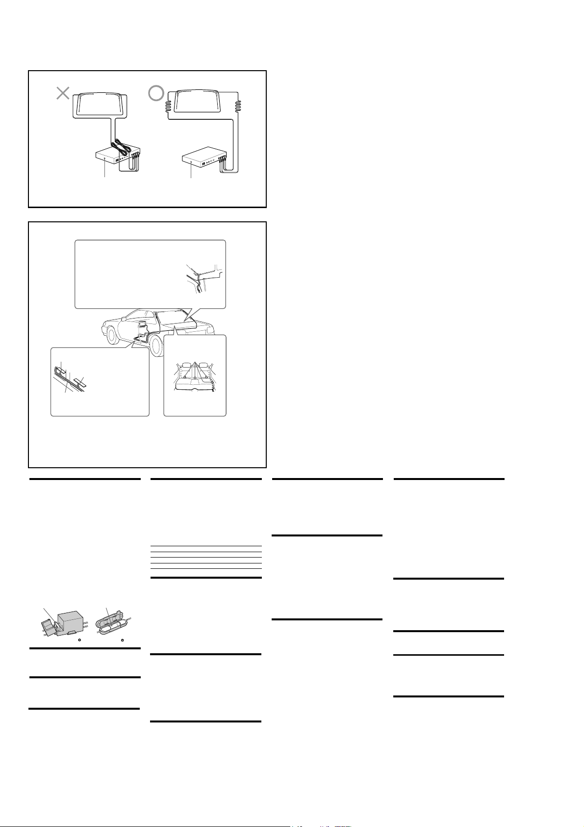
Peeling off covering paper on
bottom of aerial and sticking aerial
onto mounting surface (7-3)
Stick the aerial onto the mounting surface, with the rods
extended straight.
Tip
Before attaching the aerials, make sure that the installation surface is
clean.
Precautions on TV aerial installation
•Mount the aerials only on the inside of the rear window.
•Do not install the aerials in locations which may obstruct the
driver’s view.
•Be sure to connect the power supply lead to the ACC circuit.
•Keep the TV aerial cables as far away as possible from wiring
for an external amplifier and rear speakers.
Routing TV aerial cables (8-1)
Refer to the wiring diagram q;.
Notes
•Pull out the TV aerial rods as much as possible, but take care that
the rods do not cross or touch each other.
•In some cars, the shape or size of the rear window or the opening
of the rear gate may prevent installation of the aerials. For details,
consult your dealer.
Connecting TV aerial cables to TV
tuner unit (8-2)
Dealing with excessive TV aerial
cable length (9)
If you coil the aerial cable and place it in the vicinity of the TV
tuner unit, noise may occur. Do not coil the cable, and keep it as
far as possible from the TV tuner unit.
Wiring (q;)
If cables become tangled with the gear shift lever or other
controls, there is a severe risk of accident.
When using the Media Center main unit or the monitor, keep
the RCA interconnects as far away from the aerial cables as
possible. Otherwise noise may appear on the TV picture.
9
q;
TV tuner unit XT-P50V
Fernsehtuner XT-P50V
Scuff plate
Abriebschutz
Aerial cables
Antennenkabel
Scuff plate
Abriebschutz
Remove scuff plate and route
cables under carpet.
Entfernen Sie den Abriebschutz
und verlegen Sie die Kabel
unter dem Teppich.
Rear seat cushion
Hintere Sitzbank
Secure with tape under seat.
Mit Klebeband unter dem Sitz
befestigen.
TV tuner unit XT-P50V
Fernsehtuner XT-P50V
Hatchback type car
Secure slack parts of the cable with cable clampers, so that the
cable cannot get caught in the door. Determine the optimum
position for the ground plate before attaching it.
Fahrzeugtyp mit Heckklappe
Befestigen Sie durchhängende Kabelteile mit Kabelschellen, so
dass das Kabel nicht in der Klappe eingeklemmt wird. Legen Sie
die optimale Position für die Masseplatte fest, bevor Sie sie
anbringen.

5
XT-P50V
OSD ADJUSTMENT
Connection:
Adjusting Method:
1. Connect the PAL pattern generator to the INPUTVIDEO jack
(J104) on the HIDEAWAY board.
2. Connect the oscilloscope to the TP139 on the HIDEAWAY
board.
3. Adjust the RV100 on the HIDEAWAY board so that the clamp
voltage of the waveform on the oscilloscope becomes 1.5 ±
0.1 V.
Adjusting and Connnecting Location: HIDEAWAY Board
SECTION 3
ELECTRICAL ADJUSTMENTS
DIVERSITY VCO FREQUENCY ADJUSTMENT
Connection:
Adjusting Method:
1. Connect the TP131 and GND on the HIDEAWAY board with
to activate the test mode.
2. Connect the frequency counter to the TP130 on the
HIDEAWAY board.
3. Adjust the CT100 on the HIDEAWAY board so that the value
of the frequency counter becomes 15.625 ±0.02 kHz.
Adjusting and Connnecting Location: HIDEAWAY Board
+
–
TP130
TV Tuner Unit
(XT-P50V)
frequency
counter
+
–
PAL pattern
generator
TP139
TV Tuner Unit
(XT-P50V)
oscilloscope
INPUT
VIDEO jack
(J104)
SECTION 2
TEST MODE
MICROPROCESSOR VERSION CHECK
Checking Method:
1. Set TV SYSTEM switch of XT-P50V to 2.
2. Connect XAV-7W and turn on the power for OFF screen sta-
tus.
3. Press the preset [4] button on the wireless remote commander
(RM-X118*) , press the preset [5] button next, then press the
preset [2] button for more than 2 seconds.
4. Switch mode of TV1, press the preset [6] button on the wire-
less remote commander (RM-X118*) to call No.6.
5. “21ch” is displayed on upper right of the screen and version of
the microprocessor is indicated below.
Note: When the power is turned off after the above is executed (just after
turning off, reset is executed), both SONY BUS connected/SONY
BUS disconnected status become initialized status. (TV ch becomes
factory shipping setting)
*) RM-X118 (Part No. 1-477-110-22) is wireless remote com-
mander which is an accessory of XAV-7W.
1.5
±
0.1 Vp-p
DC 0V

6
XT-P50V
Adjusting and Connecting Location:
– HIDEAWAY BOARD (Component Side) –
J104
INPUT VIDEO
jack
RV100
OSD Adjustment
CT100
Diversity VCO
Frequency Adjustment
– HIDEAWAY BOARD (Conductor Side) –
TP139
TP130
TP131

XT-P50V
77
SECTION 4
DIAGRAMS
4-1. BLOCK DIAGRAM – AUDIO Section –
1
2
3
4
ANT8
ANT7
ANTENNA
SWITCHING
OUTPUT
DRIVER
22 VDIN
23 C. SYNC
1EO
2VCOIN
16
15
14
13
ANT1
ANT2
ANT3
ANT4
ANT5
ANT6
ANT7
ANT8
V-SYNC
SEPARATOR
DIGITAL SIGNAL
PROCESSOR
ELECTRICAL
FIELD
STRENGTH
JUDGEMENT
24
VIDEO
COMPOSITE
SYNC
SEPARATOR
PHASE
COMPARATOR
VCO,
1/32
4
CREF
CT100
DIVERSITY VCO
FREQUENCY
DIVERSITY ANTENNA
CONTROL
IC102
5
+B 9V,
25mA
6
+B 5V,
35mA
7
+BT
31V
13
+B 9V,
150mA
14
A OUT
– 14dBs
9
DATA
8
CLOCK
10
CE
TV TUNER UNIT
TU100
1
ANT1
2
ANT2
3
ANT3
4
ANT4
31 30 29
PLLDAT
PLLCLK
PLLCE
52 3
INPUT
CLUMP
11 13
LINE AMP, INPUT SELECT SWITCH
IC111
16 2
SW2
SW1
R-CH
15 IN2A+
R-CH
R-CH
MUTING
Q114
R-CH
MUTING
CONTROL SWITCH
Q120, 121
46
A SEL
48
AMUTE
B
SEL
SYSTEM CONTROLLER
IC108 (1/3)
AFT
NICAM
• SIGNAL PATH
: AUDIO (AUX)
: AUDIO (TV)
: VIDEO (TV)
ANT IN
INPUT
L
R
AUDIO
J103 (1/2)
(Page 8)
A
VIDEO
(Page 8)
OUTPUT1
L
R
AUDIO
J102 (1/2)
R-CH
OUTPUT2
L
R
AUDIO
J104 (1/2)
IN2B+
+31V
+5V
+9V
L102
L101
L103
• R-ch is omitted due to same as L-ch.
ANTENNA 4
SWITCH
Q105
ANTENNA 3
SWITCH
Q103
ANT6
ANTENNA 2
SWITCH
Q101
ANT5
ANTENNA 1
SWITCH
Q100
+5V
L115
17
NICAM
16
AFS
18
VIDEO
OUT
110
H.P.F. VCA PULSE
DET TRIGGER GATE
L.P.F. PILOT
CANCEL
NOISE CANCELLER
IC104
BUFFER
BUFFER
NC
IN
NC
OUT
BUFFER
OUT2 GROUND
ISOLATOR AMP
IC117
D128
D126
MUTING
CONTROL SWITCH
Q115
B+5V
D101
MUTING
Q119
R-CH
D129
GROUND
ISOLATOR AMP
IC120
R-CH

XT-P50V
88
4-2. BLOCK DIAGRAM –VIDEO Section –
S101
SIGNAL SELECT
OUT
50
VATT2
1
7
J103 (2/2)
VIDEO AMP
IC106
ON SCREEN DISPLAY
CONTROLLER
IC110
• SIGNAL PATH
: VIDEO (AUX)
: VIDEO (TV)
A
VIDEO
(Page 7)
VIDEO
OUTPUT1
J104 (2/2)
VIDEO
OUTPUT2
2
VIN
SW1
SYSTEM CONTROLLER
IC108 (2/3)
VOUT
1
7
VIDEO AMP
IC118
2
VIN
SW1
VOUT
23
XOUT
22
XIN
X100
8MHz
65
SDA
SCL
EEPROM
IC114
4544
SDA
SCL
47
VMUTE
B
SEL
(Page 7)
1
3
7
VIDEO SELECT SWITCH,
VIDEO AMP
IC109
INPUT
VIDEO
2
VIN
10 CVIN
VIN2
4CTL3
SW1
V OUT
8
CV
19
HOR
J103 (2/2)
27 26 54
CLK
CE
AC
OSD CLK
28
DATA
OSD DATA
OSD CE
21 20
HSYNC
VSYNC
AC
5
4
3
6
DATA
CLK
CE
AC
SIN
SCK
CS
AC
IC113
X101
4.434MHz
17
OSCIN
OSD
RV100
OSD
CONTROL
Q110
D142
SW100
TV SYSTEM
1
2
3
M+5V
35 34
SEL 3
SEL 2
33
SEL 1
25
IR IN
SWITCHING
IC188
C
SIRCS
(Page 9)
IC121(1/2)
IC121(2/2)
OTHERS
DVX-100
S100
SIGNAL SELECT
IN
XVM-R75
OTHERS
J101
REMOTE SIGNAL
OUT
J100
REMOTE SIGNAL
IN
IR BUFFER
IC115
+5V
TH101
6
8
7
L.P.F.
V SYNC
SEPARATOR
SYNC
SEPARATOR
HSY VIN
VSY
SYNC SEPARATOR
IC123
VCO PHASE
COMP

XT-P50V
99
4-3. BLOCK DIAGRAM – BUS CONTROL/POWER SUPPLY Section –
L109
BUS
DATA
2
6
5
4
3
SIRCS
CLOCK
DATA
BUSON
7
+B
BATT
RESET
4
6
11
10
9
BUS
CLK
2 13
BUS ON
IN
7 8
BUS
RESET
12 1
LINK OFF
RESET
SWITCH
CLK OUT
DATA OUT
DATA IN
BUS ON
BUS ON OUT
RESET
SONY BUS
INTERFACE
IC101
2
6
5
4
3
SIRCS
CLOCK
DATA
BUSON
RESET
7
BATT
BUS ON/OFF
SWITCH
Q109
6
9
11
10
16
LINKOFF
UNI CLK
UNI SI
UNI SO
BUSON
18
VPP
15
13
49
12
19
RESET
ACC IN
7
6
4
5
2
1
RESET
BUSY
OE
SCLK
SDA
VPP
CN101
SYSTEM CONTROLLER
IC108 (3/3)
CONTROL
IN
(SONY BUS)
CN100
CONTROL
OUT
(SONY BUS)
CN103
(FOR CHECK)
TH100
13
14
4
3
16
ERROR
AMP
ERROR
AMP
PWM
COMPARATOR
OUTPUT
CIRCUIT
PWM
COMPARATOR
OUTPUT
CIRCUIT
REFERENCE
VOLTAGE
−IN2
+IN2
−IN1
+IN1
VREF
OSC
21
RTCT
POWER CONTROL
IC100
7
9
10
B+ SWITCH
Q102, 106
F100 3
BATT
1REM
(ACC)
L100
POWER DC 12V
CN102
+5V
+9V
+8V
+31V
+8V
REGULATOR
IC105
DC/DC
CONVERTER
IC103
F101
REGULATOR 51
+5V REGULATOR,
BATTERY CHECK
IC116
VOLTAGE
DETECT
4
VINVOUT
VOR
D124
D102
D143
B+5V
D121
SWITCHING
REGULATOR
Q112, 200 (1/2)
SWITCHING
REGULATOR
Q111, 200 (2/2)
+3.3V
REGULATOR
IC107
+3.3V
OUT1
OUT2
VCC
37POWER
4
17BUCKUP
+B
M+5V
SONY BUS
INTERFACE
B+
VOLTAGE
DETECT
Q104
VOLTAGE
DETECT
Q116, 117
B+5V
SDA
SCLK
OE
BUSY
39 SONYBUS
SONY BUS
DETECT
Q122
C
SIRCS
(Page 8) L111
L108L110
+9V
REGULATOR
IC200
RESET SIGNAL
GENERATOR
IC112

XT-P50V
1010
4-4. NOTE FOR PRINTED WIRING BOARD AND SCHEMATIC DIAGRAMS
Note on Printed Wiring Board:
•X: parts extracted from the component side.
•Y: parts extracted from the conductor side.
•: Pattern from the side which enables seeing.
(The other layers' patterns are not indicated.)
Note on Schematic Diagram:
•All capacitors are in µF unless otherwise noted. pF: µµF
50 WV or less are not indicated except for electrolytics
and tantalums.
•All resistors are in Ωand 1/4W or less unless otherwise
specified.
•C: panel designation.
•A: B+ Line.
•H: adjustment for repair.
•Power voltageis dc 14.4V and fedwith regulated dc power
supply from BATT and REM (ACC) cord.
•Voltages and waveforms are dc with respect to ground
under no-signal (detuned) conditions.
no mark :TV mode
•Voltages aretakenwith aVOM(Input impedance 10MΩ).
Voltage variations may be noted due to normal produc-
tion tolerances.
•Waveforms are taken with a oscilloscope.
Voltage variations may be noted due to normal produc-
tion tolerances.
•Circled numbers refer to waveforms.
•Signal path.
E: AUDIO (TV)
a: VIDEO (TV)
F: AUDIO (AUX)
L: VIDEO (AUX)
•Waveforms
1IC100 1(CT)
2IC100 7(OUT1), Q111 (Base)
0.7 Vp-p
4.9 µs
3IC100 q; (OUT2), Q112 (Base)
13.2 Vp-p
4.8 µs
13.4 Vp-
p
4.8 µs
Caution:
Pattern face side: Partsonthepattern faceside seen from
(Conductor Side) the pattern face are indicated.
Parts face side: Parts on the parts face side seen from
(Component Side) the parts face are indicated.
4Q112 (Emitter), Q200-1 (Gate)
12 Vp-
p
4.8 µs
5Q111 (Emitter), Q200-2 (Gate)
12 Vp-
p
4.8 µs
6Q200-1 (Drain)
15 Vp-
p
4.8 µs
7Q200-2 (Drain)
14.8 Vp-p
4.8 µs
8IC103 2(OSC)
36.8 Vp-
p
52.5 µs
3 Vp-
p
226 ns
9IC110 qj (OSCIN)
q; IC113 2
3.4 Vp-
p
226 ns
qa IC113 3
3.6 Vp-
p
226 ns
qs IC113 5, 6
3.5Vp-p
226 ns
qd IC108 wd (XOUT)
5.1 Vp-
p
125 ns

XT-P50V
1111
4-5. SCHEMATIC DIAGRAM – HIDEAWAY Board (1/3) – • See page 10 forWaveforms. •See page 16 for IC Block Diagrams.
R108R301
C276
R102
R103
R105
C106
C107
L102
L101
C111
D110
C113
L103
C118
C275
C123
C268 C269L115
L104
R218 R296
R297
C104
C103
C102
C101
R154
R153
R120
C115
C121
C114
C119
R121
C117
R135
R134
R133
R132
C142
CT100
R131
TP129
R130
R136 C143
C144
C133
C126
R126
C175
C180
C167
R160
C162
R168
C185
C189
C192
R295
C196
TP123 TP120
C100
D100
TP100
TP103
TP102
Q106
Q102
C108
R114
R113
C110
C112
R119
C127 C131
C128
C130
C129
R127 R129
R128
C139
C136
R138
Q112
Q111
R139
R148
R101 R300
Q104
D117 C163 R161
R162
R163
L108 L110
D118 C164
L109
R166
R165
R164
R167
L111
C170
C173
TP137
D119
TP136
C168C153
IC105
L107
R178
R107 R110
R109
C105
L105
C134 C135 C138
R106
Q117
Q116
D128
R141 C148
C193 C197
R188
R189
TP138
Q200(2/2)
Q200(1/2)
IC100
CN102
R150
R144
C146
R142
R115
C165
R117
C116
R298
IC102
C147
R143
IC200
F101
IC103
Q115
Q107
D143
F100
IC104
R122
R123
R124
R125
TP130
L100
R100
Q101
Q100
Q103
Q105
C155
C160
R158
TP131
C140
C169
C171
C166C156
D102
C109
C248
C122
F1
220k220k
0.1
10k
10k
10k
100 16V
100 10V
0.01
MA8300-H
47 50V
39 16V
39 16V
0.022
22p 100p
00
0
1000p
1000p
1000p
1000p
0
0
47k
0.022
10
25V
0.001
0.0033
220
0.022
2.2k
2.2k
2.2k
2.2k
10p
22p
12k
33k
22k 0.01
100p
0.022
0.015
4.7k
0.01
10 25V
2200p
12k
0.047
15k
0.1
0.022
0.1
10k
0.1
3300
25VZSA5MA27
UN2111-TX
UN2211-TX
330p
4.7k
10k
330p
0.001
4.7k
0.01 10
25V
0.001
330p
0.1
4.7k 4.7k
15k
0.01
100 16V
1.2k
FMY1A-T148
FMY1A-T148
1.2k
220
2.2k 1k
UN2211-TX
SFPB-74V 100
16V 3k
100
22k
SFPB-74V 100
16V
100
220
3k
12k
39
16V
0.01
1SR154
100
16V
10
25V
BA08FP
10k
47k 4.7k
47k
1
1.2mH
0.1 47
16V 0.022
4.7k
2SC2412K
UN2211-TX
MA152WK
-TX
1k 4.7
63V
0.1 100
16V
5.1k
33k
UPA1853GR-
UPA1853GR-
TL1451ACDB
3P
1k
220
1
330
15k
10
25V
100k
0.01
0
CM0018AM
1
330
BA00ASFP-E
315mA 63V
TK11819M
UN2111-TX
2SC2412K
MA8068-L
2A 63V
TA2005SN
470
470
470
470
10k
2SA1037AK
2SA1037AK
2SA1037AK
2SA1037AK
0.1
0.047
15k
10
25V
0.01
100
16V
0.010.01
MA8180-M
2200p
2200p
2200p
5A
32V
A1
A2
A3
A4
B1
B2
B3
B4
B5
B6
B7
B8
5V
5V
31V
31V
5V
9V
8V
+B
9V
8V
PLLCLK
PLLDAT
PLLCE
AFT
NICAM
ANT5
ANT6
ANT7
ANT8
ANT5
ANT6
ANT7
ANT8
GND
BATT
REM(ACC)
VIN
OSC
DK
TI
GND
VOUT
AGC
DATA
CLOCK
ANT1
ANT4
ANT3
ANT2
+B_9V,25mA
+B_5V,35mA
+BT_31V
CE
+B_9V,150mA
GND
AFS
NICAM
VIDEO_OUT
LOCK_ACT_H
A_OUT_-14dBs
NC_IN
REF
NF
BYPASS
AGC
PW
GND
VCC
GATE
NC_OUT
LPF_OUT
PILOT_IN
GND
CTL
VCC
OUT
C
ADET4
ADET3
ADET2
ADET1
TEST1
NSOUT
DGND
CREF
RREF
VCOIN
EO
AGND
ANT4
ANT3
ANT2
ANT1
RES
DVDD
AVDD
VMODE
TEST2
VDIN
C.CYNC
VIDEO
(CHASSIS)
(CHASSIS)
(CHASSIS)
(CHASSIS)
(1/3)
+8V REGULATOR
I
G
+9V REGULATOR
DC/DC CONVERTER
SWITHING REGULATOR
S
S
-2
-1
-2
-1
SWITCH
MUTING CONTROL
ACCESSORY
CHECK
DETECT
DETECT
Q104,116
Q110,111,200
Q102,106
B+ SWITCH
POWER CONTROL
NOISE
CANCELLER
DIVERSITY ANTENNA
CONTROL
ANTENNA 4 SWITCH
Q105
Q103
ANTENNA 3 SWITCH
Q101
ANTENNA 2 SWITCH
Q100
ANTENNA 1 SWITCH
TV TUNER UNIT
(V5-E60CT)
TU100
4
3
2
1
ANT IN
REM(ACC)
GND
BATT
O
VOLTAGE
VOLTAGE
22µH
22µH
22µH
22µH
4.7µH
300µH
68µH22µH
47µH22µH
22µH
(Page 12)
(Page 13)

XT-P50V
1212
4-6. SCHEMATIC DIAGRAM – HIDEAWAY Board (2/3) – • See page 10 forWaveforms. •See page 16 for IC Block Diagrams.
C176
D101
R172
J104
J102
J103
D132
D131
D130
D135
D134
D138
R279
D133
C263
C264
C260
C261
R276
R275
R273
R274
R151
R280D137
C266 C265
Q120
D120
D116
D115
C184
C183
D122
R278
R277
C253 R270
Q119
Q118
C258
R266
R269
R140
D129
Q121
C178
C182
C181
R174
C259
C158R169 R290
C150
R284
R171
IC118
C232
C254
R159
C149R282R157
C200
R281
IC106
C132 C151
C209R156
C201
R213
C145
R145
C244
L114
R261
C154
R137
R257
R250
C229
C243
C223
TP140TP139
IC110
C221
C208R221C206
C204
C205
C207
R299
L113
C238C230
R254 R260
R258R255
R249
R242
R239
C222R247
R197
R200 R256R251
R252 R259
C256
R248
C255
R175
R182
C177
R204
C227 C237
R244
C220
C174
R263
C247C219R265C202
R262
C199
R243
L116
R104
D142
R267
R268
C120
C226
R176
Q114
Q113 R180
R181
IC120
RV100
C234
R152
IC117
C251
C152
C203 R220
R170
IC109
IC107
IC113
R302
X101
C241C240
Q110
R264 C218
IC123
IC111
C262
R179
R177
R272
R271
220
10V
MA8039-L
10k 3P
3P
3P
MA3091WK
MA3091WK
MA3091WK
MA3091WK
MA3091WK
MA3091WK
75
MA3091WK
100p
100p
100p
100p
470
470
10k
10k
1
0MA111
47
16V
0.47
50V
UN2211-TX
MA3091WK
MA3091WK
MA3091WK
100p
100p
MA3091WK
0
0
220
10V
470
DTC314TK-T
DTC314TK-T
10
25V220
220
2.2k
MA8039-L
UN2111-TX
100
10V
10
25V
10
25V220
10 25V
0.011k 1M
10
25V
1M
10k
NJM2244M
10
25V
100
10V
10k
0.011M1k
10
25V
1M
NJM2244M
0.01 0.01
0.010
0.01
1k
10
25V
2.2k
0.01
1M
0.1
10k
470
1k
0.22
10
25V0.01
M35054-001
0.1
470p1.5k0.22
1
10 25V
0.01
220
10
25V
10
25V
10k 10k
1k1k
1k
2.2k
2.2k
0.0122k
0
01k1k
10k 10k
10
25V
22k
10
25V
220
0
10
25V
0
10
25V
10
25V
22k
100
10V 10
25V
0
0.01560p100k4.7
1k
3900p
82k
4.7k
MA152WK
-TX
10k
10k
470
10V
0.01
470
DTC314TK-T
DTC314TK-T 0
0
M5280FP-TP
10k
10
25V
0
M5280FP-TP
100
10V
470
10V
470
10V 75
75
MM1228XF
NJM2370
TC7WU04FU
6.8k
4.434MHz
27p33p
2SC2412K
330k 1
MM1108XFBE
NJM2123V
10
25V
15k
15k
15k
15k
A1
A2
A3
A4
C1
C2
C3
C4
+B
5V
8V
8V
5V
8V
5V 5V
BUS_R
BUS_L
OSD_CLK
OSD_DATA
OSD_CE
AC
BUS_L
BUS_R
HSYNC
VSYNC
VIN
SW1
VIN2
CTL3
GND
VOUT
VCC
IN3
CP1
TESTA
CS
SCK
SIN
AC
VDD2
CV
LECHA
CVIN
VDD1
HOR
CP2
OSCIN
VSS
P1
P0
TESTB
TESTC
VSS
CBP
VOUTVIN
VIN
SW1
VIN2
CTL3
GND
VOUT
VCC
IN3
VIN
SW1
VIN2
CTL3
GND
VOUT
VCC
IN3
VCC
GND
VIN
SC
VCO
LPF
VSY
HSY
GND
VCC
GND
SWR
IN2B+
IN2B-
OUT2
IN2A-
IN2A+
SW2
VCC
IN1A+
SW1
IN1A-
OUT1
IN1B-
IN1B+
SWC
VCC
GND
VCC
GND
(CHASSIS)
(CHASSIS)
(2/3)
VIDEO
L
R
AUDIO
INPUT
Q118,119
MUTING
Q120,121
MUTING CONTROL
SWITCH
MUTING
Q113,114
GROUND
ISOLATOR
AMP
GROUND
ISOLATOR
AMP
VIDEO AMPVIDEO AMP
VIDEO SELECT
SWITCH,
VIDEO AMP
REGULATOR
+3.3VG
INVERTER
ON SCREEN DISPLAY CONTROLLER
OSD CONTROL
SYNC
SEPARATOR
LINE AMP,
INPUT SELECT
SWITCH
VIDEO
L
R
AUDIO
OUTPUT1
VIDEO
L
R
AUDIO
OUTPUT2
VM1
VM2
VM1
VM2
22µH
22µH
22µH
(Page 11)
(Page 13)

XT-P50V
1313
4-7. SCHEMATIC DIAGRAM – HIDEAWAY Board (3/3) – • See page 10 forWaveform. •See page 16 for IC Block Diagrams.
D114
TP106
TP114
TP112
TP105
TP101
TP119
TP104
D108
D109
R118
D103
D104
D105
D107
D111
D112
D113
C124
C125
L106
TP135
TP134
TP133
TP132
R187
R185
R184
C190
TP145
L112
R225
R217
R224
R227
C271
R283
TP152
TP151
R194
D126
TP161
R202
R199
R206
R207
R210
R212
R215
R216
R222
R234
R233
R232
R231
R230
R229
R228
X100
C267
C213
R291
R293
TP800
C273
C217
C216
R235
C233
C225
C228
IC112
IC115
IC114
C246 D140
C159
D124
C245
C157
C250
R253
R287
D123
R116
R292
C141
C272R289R288
TP117
TH100
R211
C198
C172
IC188 R223
TH101 TP803
D127
CN103
TP169
TP168
D125R214
TP801
S101
S100
C242
IC121
R241R238
R226 C224
SW100
IC101
D121
TP167
TP153
CN100
CN101
TP179
J100
J101
TP804
TP802
IC116
C215C212
R201R195
IC108
Q109
Q122
C249
C187
C186
C137
1SS355
MA8180-M
MA728
220
MA8180-M
MA8180-M
MA8180-M
MA8180-M
MA728
MA728
MA728
0.01
0.0047
33
0
0
47 16V
100k
100k
100k
100k
0.01
0
100
1SS355
33
33
100
100
100
33
33
33
100
100
100
100
100
100
100
0
8MHz
0.01
0.1
47k
100k
0.01
27p
22p
100
10
25V
0.1
5V
0.1
PST9145
TC7S08F
AT24C08
10
25V 1SS355
0.1
1SS355
0.1
0.1
10
25V
47k
100k
MA729
-TX
47k
4.7k
10
25V147k4.7k
100k
0.01
0.01
TC7S32F 100k
MA3091WK
8P
MA3091WK100k
0.01
TC7WU04FU
4.7k4.7k
1k 0.1
BA8272F
MA721WA
8P
8P
S-875271C
330p330p
100100
M38039FFFP-081
UN2111-TX
2SC2412K
0.1
0.01
0.01
0.01
B1
B2
B3
B4
B5
B6
B7
B8
C1
C2
C3
C4
+B
5V
5V
PLLCLK
PLLDAT
XRST
SDA
SCLK
BUSY
CLKI
DATO
DATI
BUSI
DATI
DATO
BUSI
CLKI
BUSY
SCLK
SDA
OE
XRST
OSD_CLK
OSD_DATA
OSD_CE
PLLCE
VPP
VPP
LINKOFF
LINKOFF
AC
HSYNC
VSYNC
NICAM
AFT
OE
OE
BUSY
SCLK
SDA
GND
VPP
VDD
RESET
RESET
RESET
SIRCS
SIRCS
CLOCK
CLOCK
DATA
DATA
BUSON
BUSON
BATT
BATT
GND
GND
NC
NC
(CHASSIS)
VCC
GND
(3/3)
OUT
IN
REMOTE
SIGNAL
FOR
CHECK
INVERTER
-1 -2
-1 -2
S100
SIGNAL
SELECT
IN
OTHERS
XVM-R75
SIGNAL
SELECT
OTHERS
S101
OUT
DVX-100
IR BUFFER
G
V
SWITCHING
1
2
3
4
5
VCC
WP
SCL
SDA
A0
A1
A2
GND
EEPROM
+5V REGULATOR,
BATTERY CHECK
VOUT
GND
VPF
VIN VOR
RESET SIGNAL
GENERATOR
VCC OUT
NC
SUB
GND
TV SYSTEM
321
SYSTEM CONTROLLER
BUS ON/OFF
SWITCH
SONY BUS
DETECT
SONY BUS
INTERFACE
OUT
IN
CONTROL
(FOR SONY BUS)
22µH
22µH
(Page 12)
(Page 11)

XT-P50V
1414
4-8. PRINTED WIRING BOARD – HIDEAWAY Board (Component Side) –
L101
L103
L102
Q100
R100
Q101
R102
Q103
R103
Q105
R105
C268
L115
C269
R217
R224
R226
D127
D125
IC108
IC102
IC115
C242
IC101
R125
R124
R123
R122
C116
R120
C119
C114
R121
C117
R130
CT100
C144
R133
R134
R135
L104
D103
D104
D105
R116
D113
C124
D112
D111
C125
C137
R195
R201
R206
R207
R210
R212
R215
R216
R222
C213
R227
R225 R194
R199
R202
R283
R187
R185
C187
C186
L112
R287
R238
R241
R118 D108
D109
Q109
D114
R288
R289
R291
Q122
R292
IC111
Q119 Q118
R266
R269
C185
C196
R295
IC100
C108
R113
C110
R115
C130
R128
Q102
R114
R119
C129
R127
R129
F100
Q111
Q112
R142
R144
R138
R139
R143
R148
L108 L109
L111
R166
R165
R164
R163
R162
R161
R178
C193
R189
R188
C170
R101
D102
R117
Q107
R110
R109
R106
R107
F101
IC103
C138
C134
R141 R150
R252
R254
C209
C201
R213
D129
R280
D137
Q121
Q120
D128
IC110
C206
IC113
L114
IC114
C224
IC112
C228
IC116
C245
D121
D124
C249
C146 C147
C272
R253
Q106
R137
C154
IC107
R260
R140
R145
R156
C132
C151
R157
R159 R171
R278 R277
L107
L110
R136
C143
R132
C128
C112
C127
R167
R131
R259
C207
C244
Q113
Q114
R181 R180
Q110
R172
R104
R184
D126
Q115
R220
C173
D119
C155
C221 R257
R228
R151
D132
R279
C157
C159
D140
R270
D138
R169
C189
C223
C226
C229
R250
C204
R221
C208
RV100
IC121
C172
TH101
R197
R200
R204
IC188
C198
R244
C222
R248
R255
R258
R251
C105
R211
R214
R223
R247
R265
R243
R262
R267
R268
R263
R264
C219
C199
C218
C202
L116
C247
C273
C267
R229
R231
R233
R235
R234
R232
R230
C215
C212
R175
D101
C158
C149
R281
R282
R284
R290
IC106
IC117
IC109
D142
C118
C275
Q200
D107
R299
IC123
IC118
D100
R108
R301
R300
D143
Q117
Q104
Q116
R256
(COMPONENT SIDE)
HIDEAWAY BOARD
1-686-471- 11
1 2 3 4 5 6 7 8 9 10 11 12 13 14 15
A
B
C
D
E
F
G
H
I
J
K
L
D100 L-1
D101 C-14
D102 E-1
D103 C-4
D104 C-3
D105 C-3
D107 C-3
D108 C-2
D109 C-2
D111 D-3
D112 D-3
D113 D-4
D114 D-2
D119 I-6
D121 G-3
D124 G-2
D125 L-4
D126 F-4
D127 K-5
D128 E-2
D129 C-11
D132 C-5
D137 G-4
D138 C-10
D140 F-3
D142 D-11
D143 E-1
IC100 K-5
IC101 D-3
IC102 J-9
IC103 H-7
IC106 D-9
IC107 E-7
IC108 F-4
IC109 E-10
IC110 F-8
IC111 D-7
IC112 D-3
IC113 E-8
IC114 G-4
IC115 K-4
IC116 G-2
IC117 D-11
IC118 D-12
IC121 K-6
IC123 H-8
IC188 K-5
Q100 K-11
Q101 K-11
Q102 K-4
Q103 J-11
Q104 F-1
Q105 J-11
Q106 J-4
Q107 E-2
Q109 D-2
Q110 G-8
Q111 J-5
Q112 J-5
Q113 C-14
Q114 C-14
Q115 E-2
Q116 F-2
Q117 E-2
Q118 C-11
Q119 C-11
Q120 G-4
Q121 G-4
Q122 D-3
Q200 J-5
•Semiconductor
Location
Ref. No. Location

XT-P50V
1515
4-9. PRINTED WIRING BOARD – HIDEAWAY Board (Conductor Side) –
CN100 CN101
TU100
C106
C113
C100
L100
IC104
TH100
C141
X100
C190
C262
C256
C255
C259
C258
C165 C180
C145
C164
C171
C168
C148
C227
C237
C232
C238
C230
C234
C203
C266
C200
X101 C243
C225
C250
CN103
C131
C163
C136
C140
C153
C233
C246
C265
C177C174
C181
C182 C150C152
C121
C197
C135
S100
S101
C120
J101
C205
CN102
C176
C253
C178
C254
C251
C107
C220
L105
D122
D115 D116
D133 D134
D135
D130 D131
R152 C260 C261
C263
R276 R274
R275
R273
C104
C103
C102
C101
R153
R154
C139
D117D118
IC200
IC105
C109
C111
D110
C133
C123
C122
R126
C126
C175
IC120
C183
R177
C184
R179
R174
R176
R170
C166
C156
R239
R242
C216
R182
D120 C264
R271 R272
L106
D123
L113
R293
C271
C115
R261
C217
R249
C162
R158
C160
R160
R168
C167
C248
C241
C240
R218
R296
R297 R298
C276
C142
R302
C169
J100
12
HIDEAWAY BOARD
(CONDUCTOR SIDE)
1-686-471- 11
AUDIO
R L
J104
VIDEO
OUTPUT2
AUDIO
R L
J102
VIDEO
OUTPUT1
AUDIO
R L
J103
VIDEO
INPUT
(CHASSIS)
TV TUNER UNIT
(CHASSIS)
4
ANT IN
3 2 1
TP131
TP130
-1
-2
-1
-2
OUT IN
S101 S100
SIGNAL
SELECT
OTHERS DVX-100 OTHERS XVM-R75
OUT IN
REMOTE
SIGNAL
POWER DC 12V
12 3
F1 YEL
BLK
BLU
BATT
GND
REM (ACC)
(CHASSIS)
3
5
4
2
1
2
3
1
TP139
(FOR CHECK)
TV SYSTEM
SW100
1
2
3
(CHASSIS)
OUT IN
CN100 CN101
CONTROL
(FOR SONY BUS)
1 2 3 4 5 6 7 8 9 10 11 12 13 14 15
A
B
C
D
E
F
G
H
I
J
K
L
M
+
D110 H-5
D115 B-2
D116 B-3
D117 I-12
D118 I-12
D120 C-4
D122 B-4
D123 D-12
D130 C-9
D131 C-10
D133 B-6
D134 B-7
D135 C-8
IC104 F-7
IC105 G-12
IC120 D-3
IC200 H-12
•Semiconductor
Location
Ref. No. Location

XT-P50V
1616
•IC Block Diagrams
IC100 TL1451ACDB IC101 BA8272F-E2
REFERENCE
VOLTAGE
LATCH
TRIANGLE
OSCILLATOR
VERF.
+2.5V
+2.5V
+
–
U.V.L.O
–
+
+
–
12 3 45 6 7 8
91016 15 14 13 12 11
PWM
COMPA-
RATOR2 OUTPUT2
OUTPUT1
GND
PWM
COMPA-
RATOR1
VERF
SR R
VERF
VERF
ERROR
AMP2
ERROR
AMP1
VREF/2
SHORT
CIRCUIT
PROTECTION
COMPARATOR
VCC
+
REF
OUT
S.C.P
NON-INV-
INPUT2
INV-
INPUT2
FEED
BACK2
DEAD
TIME
CONTROL2
OUT2
VCC
GND
OUT1
RT
NON-INV-
INPUT1
INV-
INPUT1
FEED
BACK1
DEAD
TIME
CONTROL1
CT
12 3 45 6 7
89
10
14 13 12 11
VCC
BUS ON
LINK OFF
CLK OUT
DATA OUT
DATA IN
BUS RESET
BUS DATA
VREF
BUS CLK
GND
BUS ON IN
BUS ON OUT
RESET
RESET
SWITCH
IC102 CM0018AM
3
4
5
6
7
8
9
10
11
12
EO
VCOIN
RREF
CREF
AGND
DGND
NSOUT
OMODE
ADET1
ADET2
ADET3
ADET4
24
23
22
21
20
19
18
17
16
15
14
13
VIDEO. IN
C. CYNC
VDIN
ADV
VMODE
AVDD
DVDD
RESB
ANT1
ANT2
ANT3
ANT4
1PHASE
COMPARATOR
2
VCO 1/32
DIGITAL
SIGNAL
PROCESSOR
COMPOSITE
SYNC
SEPARATOR
INPUT CLAMP
ELECTRIC FIELD
STRENGTH
JUDGEMENT
V SYNC
SEPARATOR
NOISE SUPPRESSOR
OUTPUT DRIVER
ANTENNA
SWICTHING
OUTPUT
DRIVER
REDUCED-VOLTAGE
DETECTOR
RESET
IC103 TK11819MTL
6
5
4
1
2
3
STRAT-UP VCO REFERENCE
VOLTAGE
FEEDBACK
CONTROL
VIN
OSC
DK
VOUT
GND
T1
IC104 TA2005SN
12
11
107654321 8 9
LPF
HPF VCA
REF
TRIGGER GATE
PULSE
DET
PILOT
CANCEL
BUFF
BUFF
BUFF
BUFF
INV
AMP
PILOT
IN
LPF
OUT
OUT
GATE
REF
+B
GND
PW
AGC
BYPASS
NF
IN
IC106, 118 NJM2244M-TE2
2
SW1
3
VIN2
4
SW2
1
VIN1 8 GND
7 VOUT
6V+
5 VIN3 (MUTE)
BIAS
75 Ω
DRIVER
IC109 MM1228XFBE
1
2
3
4
8
7
6
GND
VOUT
VCC
IN3
CTL3
VIN2
SW1
VIN1
5
BIAS
IC110 M35054-001FP
1
2
3
4
5
6
7
8
9
10
CP1
TESTA
CS
SCK
SIN
AC
VDD2
CVIDEO
CVIN
LECHA
19
18
17
16
15
14
13
12
11
HOR
CP2
OSCIN
VSS
P1
P0
TESTB
TESTC
VSS
INPUT/OUTPUT
CONTORL
CIRCUIT
CLOCK
GENERATOR
CIRCUIT
DISPLAY
CONTROL
RESISTOR
DATA
CONTROL
CIRCUIT
ADDRESS
CONTROL
CIRCUIT
TIMING
GENERATOR
DISPLAY POSITION
DETECT CIRCUIT
H COUNTER
READ ADDRESS
CONTROL CIRCUIT
TIMING
GENERATOR
DIPLAY CHARACTER ROM
DISPLAY RAM
DISPLAY
CONTROL
CIRCUIT
BLINKING
CIRCUIT
NTSC
PAL
M-PAL
VIDEO
OUTPUT
CIRCUIT
PORT OUTPUT
CIRCUIT
SHIFT
RESISTOR
OSCILLATION
CIRCUIT FOR
SYNC SIGNAL
GENERATOR
SYNC SEPARATOR
CIRCUIT
20 VDD1

17
XT-P50V
IC111 NJM2123V (TE2) IC116 S-875271CUP-AHA-T2
1
2
3
4
5
6
7
8
V+
SW1
IN1 A+
IN1 A–
OUT1
IN1 B–
IN1 B+
SW C
16
15
14
13
12
11
10
9
SW 2
IN2 A+
IN2 A–
OUT2
IN2 B–
IN2 B+
SW R
GND
1
2
3
5
REGULATOR
POWER
ON/OFF
VOLTAGE
DETECT 4
PROTECT
CIRCUIT
V OUT
VSS
VPF
VOR
V IN
IC123 MM1108XFBE
2 3 41
7 6 58
VCO
V SYNC
SEP
SYNC
SEP
PHASE
COMP
H. SYNC
V. SYNC
VIN
GND
VCC
SC
VCO
LPF
3V

18
XT-P50V
4-10. IC PIN FUNCTION DESCRIPTION
•IC108 M38039FFFP-081 (SYSTEM CONTROLLER)
Pin No. Pin Name I/O Description
1, 2 N.C.O I Not used
3 AFT I Auto fine tuning detection signal input from the TV tuner unit
4ACC IN I Accessory detection signal input “L”: accessory on
5 N.C.O I Not used
6 LINKOFF O Link on/off control signal output for the SONY bus “H”: link off
7, 8 N.C.O I Not used
9UNI CLK I Serial data transfer clock signal input from the SONY bus interface
10 UNI SO O Serial data output to the SONY bus interface
11 UNI SI I Serial data input from the SONY bus interface
12 BUSY I Busy signal input terminal
13 SCLK O Serial data transfer clock signal output terminal
14 N.C.O I Not used
15 SDA I/O Two-way data bus terminal
16 BUSON I Bus on/off control signal input from the SONY bus interface “L”: bus on
17 BUCKUP I Battery detection signal input “H”: battery on
18 VPP I VPP signal input terminal
19 RESET I System reset signal input from the SONY bus interface and reset signal generator “L”: reset
For several hundreds msec. after the power supply rises, “L” is input, then it changes to “H”
20 VSYNC I Vertical sync signal input from the sync separator
21 HSYNC I Horizontal sync signal input from the sync separator
22 XIN I Main system clock input terminal (8 MHz)
23 XOUT O Main system clock output terminal (8 MHz)
24 VSS — Ground terminal
25 IR IN I IR data input
26 OSD CE O Chip enable signal output to the on screen display controller “H” active
27 OSD CLK O Serial data transfer clock signal output to the on screen display controller
28 OSD DATA O Serial data output to the on screen display controller
29 PLLCE O Chip enable signal output to the TV tuner unit “H” active
30 PLLCLK O Serial data transfer clock signal output to the TV tuner unit
31 PLLDAT O Serial data output to the TV tuner unit
32 N.C.O I Not used
33 to 35 SEL 1 to SEL 3 I TV SYSTEM switch input terminal
36 N.C.O I Not used
37 POWER O System power supply on/off control signal output “H”: power on
38 N.C.O I Not used
39 SONYBUS I SONY bus detection signal input “L”: SONY bus connected
40 to 43 N.C.O I Not used
44 SDA I/O Two-way data bus with the EEPROM
45 SCL O Serial data transfer clock signal output to the EEPROM
46 A SEL O TV/CD changer audio selection signal output “L”: TV, “H”: CD/DVD changer
47 VMUTE O Video line muting on/off control signal output “H”: muting on
48 AMUTE O Audio line muting on/off control signal output “H”: muting on
49 OE O Output enable signal output terminal “L” active
50 VATT2 O Video line muting on/off control signal output “H”: muting on
51 N.C.O I Not used

19
XT-P50V
Pin No. Pin Name I/O Description
52 NICAM O Destination setting terminal of TV tuner unit
Normally: fixed at “L”, “H”: hong kong and south africa area models
53 N.C.O I Not used
54 AC O OSD data clear control signal output to the on screen display controller “L”: all clear
55, 56 N.C.O I Not used
57 VCC — Power supply terminal (+5V)
58 VREF I Reference voltage (+5V) input terminal (for A/D, D/A converter)
59 AVSS — Ground terminal (for A/D, D/A converter)
60 to 64 N.C.O I Not used

20
XT-P50V
5
1
2
3
4
7
not supplied
not supplied
#1
#1
#1
#2
6
F1
SECTION 5
EXPLODED VIEW
•Items marked “*” are not stocked since they
are seldom required for routine service. Some
delay should be anticipated when ordering
these items.
•Accessories are given in the last of the elec-
trical parts list.
NOTE:
•-XX and -X mean standardized parts, so they
may have some difference from the original
one.
•Color Indication of Appearance Parts
Example:
KNOB, BALANCE (WHITE) . . . (RED)
↑↑
Parts Color Cabinet's Color
Ref. No. Part No. Description Remark Ref. No. Part No. Description Remark
11-590-519-21 CORD (WITH CONNECTOR) (BUS)
21-824-336-11 CORD, CONNECTION (RCA)
3A-3274-571-A HIDEAWAY BOARD, COMPLETE
43-376-464-11 SCREW (+PTT 2.6X6), GROUND POINT
51-824-545-11 CORD, CONNECTION (STEREO MINI)
61-824-788-11 CORD, CONNECTION (POWER)
71-543-653-11 CORE ASSY, BEAD (DIVISION TYPE)
F1 1-532-796-11 FUSE (BLADE TYPE) (AUTO FUSE) (5A/32V)
#1 7-685-792-09 SCREW +PTT 2.6X6 (S)
#2 7-685-534-19 SCREW +BTP 2.6X8 TYPE2 N-S
Other manuals for XT-P50V
2
Table of contents
Other Sony TV Tuner manuals

Sony
Sony WRR-802A User manual

Sony
Sony FDT-5BX5 User manual

Sony
Sony XT-DTV1 User manual

Sony
Sony PEGA-VR100K User manual

Sony
Sony SAT-HD100 User manual

Sony
Sony VGN-AX Series Guide

Sony
Sony XT-P50V User manual

Sony
Sony XT-V70 Marketing Product guide

Sony
Sony XT-V70 Marketing Product guide

Sony
Sony XT-U500V User manual