ST STEVAL-TTM001V1 User manual

Introduction
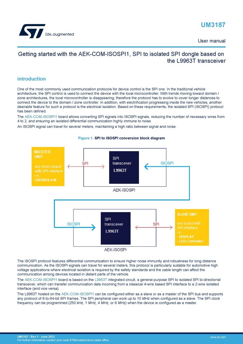
The STEVAL-TTM001V1 evaluation kit is designed to demonstrate the highly efficient ST automotive-grade 100 V STripFET F7
series Power MOSFETs and BLDC motor driver IC operating in typical automotive low voltage (car battery up to 48 V), high
current motor control applications.
The kit includes a board to sense and condition currents, and a driver board with a programmable L9907 FET driver with full
diagnostics to manage all 36 STH315N10F7 Power MOSFETs on a power board also included in the kit.
The driver board also includes an ST motor control connector to interface with any compatible ST motor control board (not
included in the kit), and various other connectors and jumpers for monitoring and protection, motor position feedback
information, and auxiliary power.
Figure 1. STEVAL-TTM001V1 evaluation kit
5 kW low voltage high current inverter for automotive motor control applications
UM2673
User manual
UM2673 - Rev 1 - January 2020
For further information contact your local STMicroelectronics sales office.
www.st.com

1Evaluation kit features
1.1 Electrical and functional characteristics
The kit features the following main characteristics:
•Power board with insulated metal substrate (IMS) hosting 36 STH315N10F7 power MOSFETS in the
H²PAK-6 (6x switch) package for automotive applications.
•L9907 automotive gate drivers to drive the power MOSFETs providing full diagnostic and programmable
parameters (cross conduction, dead time, gate current, etc.) via SPI.
• Maximum power 5 kW at 48 V.
• Isolated current sensing, bus voltage and temperature monitoring.
1.2 Target applications
The STEVAL-TTM001V1 kit is designed for applications involving motor drives for electric traction, such as:
•urban electric cars
• small city buses
• other 48V electric vehicles
UM2673
Evaluation kit features
UM2673 - Rev 1 page 2/42

2Safety and operating instructions
2.1 General terms
All operations involving transportation, installation and use, as well as maintenance, has to be carried out by
skilled technical personnel (national accident prevention rules must be observed). For the purpose of these basic
safety instructions, "skilled technical personnel" are considered as suitably qualified people who are familiar with
the installation, use, and maintenance of power electronic systems.
2.2 Intended use of evaluation kit
This evaluation kit is designed for demonstration purposes only and shall not be used for any commercial
purpose. The technical data, as well as information concerning power supply conditions, must be taken from the
relevant documentation and strictly observed.
2.3 Evaluation kit setup
• The evaluation kit must be set up in accordance with the specifications and the targeted application.
•The board contains electro-statically sensitive components that are prone to damage through improper use.
Electrical components must not be mechanically damaged or destroyed.
•Avoid any contact with other electronic components.
• During the motor driving, converters must be protected against excessive strain. Do not bend or alter the
isolating distances any components during transportation or handling.
2.4 Electronic connections
Applicable national accident prevention rules must be followed when working on the main power supply with a
motor drive. The electrical installation must be completed in accordance with the appropriate requirements. A
system architecture which supplies power to the evaluation board must be equipped with additional control and
protective devices in accordance with the applicable safety requirements (e.g., compliance with technical
equipment and accident prevention rules).
UM2673
Safety and operating instructions
UM2673 - Rev 1 page 3/42

3Evaluation kit overview
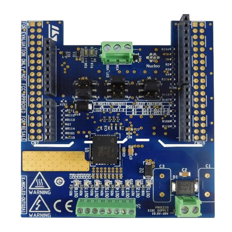
The STEVAL-TTM001V1 evaluation kit is designed to let you evaluate STH315N10F7 power MOSFETs, which
are driven by the automotive grade L9907 three phase gate driver able to provide full diagnostic and
programmable parameters via SPI. The system includes a bulk capacitor board and a current sensing board.
The STEVAL-TTM001V1 can be interfaced with any ST MCU evaluation board with embedded ST motor control
connector and ST FOC firmware library support.
This kit has been tested with the STEVAL-TTM002V1 (not included in this kit) which features an SPC560P50L3
32-bit power architecture MCU for automotive applications.
Figure 2. STEVAL-TTM001V1 block diagram
DRIVING STAGEPOWER STAGE
SPI
Motor Control
ICS
Vin
5V DC/DC
3V3 DC/DC
DRV > PW
L9907
driver
ENC/HALL
PW->DRV PW->DRV PW>DRV
12x
STH315N10F7
in H2PAK-6
-
Phase_U Phase_V Phase_W
Shunt
resistor
Shunt
resistor
Shunt
resistor
12x
STH315N10F7
in H2PAK-6
12x
STH315N10F7
in H2PAK-6
connector on top
connector on bottom
NTC
LEGEND
12V DC/DC
DRV > PW DRV > PW
UM2673
Evaluation kit overview
UM2673 - Rev 1 page 4/42

4STEVAL-CTM004V1 power board
The STEVAL-CTM004V1 power board of the evaluation kit has 36 STH31*N10F7 N-channel Power MOSFETS in
the H²PAK-6 package. A gate resistor is placed near each power MOSFET to eliminate parasitic oscillation. A
pull-down resistor between the gate and the source of each transistor helps to avoid capacitive coupling driving
the transistor and unwanted switch-on when gate is floating. A snubber RC circuit on each switch limits the rate of
voltage change during switching transitions to reduce electromagnetic interference (EMI) and losses.
two decoupling capacitors close to the switching power MOSFETs reduce ringing on the VDS and voltage stress
on the devices. The capacitors reduce voltage overshoot caused by abrupt current change in the parasitic
inductors in the circuit.
To monitor the temperature of the power board and provide over-temperature protection, three NTCs are placed
on the power board near the drain of one power MOSFET for each inverter leg.
The power section also has connectors for the driver board, with CON5 (phase_U), CON6 (phase_V) and CON7
(phase_W) for gate driving and NTC sensing, and J3 for bus voltage. The board also hosts six towers near the
bulk capacitor board connection and three towers near the motor connection.
Figure 3. Main blocks of the STEVAL-CTM004V1 power board
4.1 STH315N10F7 N-channel Power MOSFET characteristics
The N-channel Power MOSFETs use STripFET™ F7 technology with an enhanced trench gate structure for very
low on-state resistance and reduces internal capacitance and gate charge for faster and more efficient switching.
The STH315N10F7 N-channel Power MOSFET has the following features:
• Designed for automotive applications and AEC-Q101 qualified
•Among the lowest RDS(on) on the market
UM2673
STEVAL-CTM004V1 power board
UM2673 - Rev 1 page 5/42

• Excellent figure of merit (FoM)
•Low Crss/Ciss ratio for EMI immunity
•High avalanche ruggedness
Figure 4. Package and internal schematic diagram
UM2673
STH315N10F7 N-channel Power MOSFET characteristics
UM2673 - Rev 1 page 6/42

5STEVAL-CTM007V1 driver board
Figure 5. STEVAL-CTM007V1 driver board functional blocks
1. connections to power board
2. motor control connector
3. ENC/HALL connector
4. ICS connector compatible with STEVAL-CTM008V1
5. L9907 driver
6. 3V3 DC/DC regulation
7. 5V DC/DC regulation
8. 12V DC/DC regulation
11 1
5
4
37
86
2
5.1 Power supply section
The power supply section provides all the voltages necessary for the circuitry. The required input voltage is 8 to
25 V input, which is supplied through connector JP1.
The input voltage is then converted to the following voltage levels:
• +12V for gate driver section (via an A7986 which is a 3 A step-down switching regulator)
• +5V and +3.3V for the control board (via an A6902 which is a 1 A switch step-down regulator)
5.2 Bus voltage monitoring
Bus voltage monitoring is implemented across an input voltage range of 5 to 75 V.
The following table shows the measured input voltage and the corresponding voltage level sent to the ADC input
of the SPC5 microcontroller unit.
Table 1. Input voltage bus and input signal to SPC5 ADC channel
Input Voltage ADC input
48V 2.0V
75V (max value) 3.1V
5.3 Temperature monitor
Three NTCs are placed on the power section to provide temperature information, although only one NTC may be
chosen at a time. Close one of the three jumpers S1, S2 or S3 to read the temperature near the U, V or W phase,
respectively. The microcontroller monitors processed signals to determine the temperature of the driver board and
manage any overload or over-temperature conditions.
To protect the hardware from excess temperature, a safe threshold is set in SPC5-MCTK-LIB.
UM2673
STEVAL-CTM007V1 driver board
UM2673 - Rev 1 page 7/42

Table 2. NTC electrical characteristics
Symbol Parameter Test Condition Min Typ Max Unit
R-40 Resistance T = -40°C - 105.7 - kΩ
R25 Resistance T = 25°C - 4.7 - kΩ
R100 Resistance T = 100°C - 0.426 - kΩ
B B- constant T = 25°C to 50°C - 3500 - -
T Operating temp range - -40 - 125 °C
5.4 L9907 gate driver characteristics
The main features of the L9907 gate driver are listed below:
•dV/dt immunity ±50 V/ns in full temperature range
• AEC-Q100 qualified
•Supply voltage from 6 V to 54 V for working battery applications
• The device can withstand -7 V to 90 V at the FET high-side Driver pins
• Low standby current consumption
• 3.3 V internal regulator supplied by VCC pin
• Boost regulator for full RDSON down to 6 V and over voltage protection
• 3 low-side plus 3 high-side drivers
• PWM operation up to 20 kHz
• Gate driver current adjustable via SPI in 4 steps.
– Range set via external resistor.
– Maximum gate controlled current 600 mA
• Source connection to each MOSFET
• Input pin for each gate driver
RELATED LINKS
For detailed information and pin-out details regarding the L9907 gate driver, see the device datasheet
5.5 L9907 supply voltage configuration for 48 V applications
The L9907 automotive 3 phase BLDC driver has a default typical overvoltage threshold of 36 V. if 48 V is applied
to the VB pin, an OV error is triggered in the start phase with (B11) = ‘1’ in the DIAG register and the FS_FLAG
pin set to low.
As the VB pin is supplied from 48 V, the overvoltage protection VBov (B9) has to be disabled setting ‘0’ in CMD1
register. The overvoltage protection set on the boost regulator BST_C pin also needs to be disabled (default is set
to '0') by setting bit DIS_BSTov (B12) in CMD3 register to ’1’.
Note: This bit is only acknowledged if AND (EN1, EN2) = '0'. Trying to write it without lowering AND (EN1, EN2) will not
generate an SPI error, but the command will be ignored for the specific bit.
While setting CMD3 B12 to 1 disables the overvoltage protection on the BST_C pin, this solution does not allow
use of the FS_FLAG pin (which would always be low) to trigger an error in the microcontroller. This is due to the
fact that only the fault effect is disabled when VBov (B9) is set to ‘0’, while the fault is still latched in the SPI
register DIAG. Continuous polling must therefore be performed to query the device to verify whether errors are
present.
RELATED LINKS
See application note AN5124 for more details
UM2673
L9907 gate driver characteristics
UM2673 - Rev 1 page 8/42

6Bus link capacitor board and current sensing board
6.1 STEVAL-CTM005V1 bus link capacitor board
In EV inverter systems, bus link capacitors reduce ripple current and suppress voltage spikes caused by leakage
inductance and switching operations. These capacitors provide a low impedance path for the ripple currents
caused by output inductance load, the bus voltage and PWM frequency.
The bus link capacitors must sustain a ripple current given by the following formula:
ΔI0.5t= 0.25 × Vbus
f×L
Where:
• ΔI0.5t is the maximum ripple current when duty cycle is 50%
•Vbus is the bus voltage
• f is the switching frequency
• L is the load inductance.
For a very low inductance motor (worst case scenario), ΔI0.5t is about 48 ARMS (Vbus = 52 V, f = 8 kHz and
L = 12 μH). If we add 10% to ΔI0.5t and choose electrolytic capacitors with a ripple current of 2.4 A, 22 electrolytic
capacitors are required. The resulting capacitance is about 6 mF, leading to a negligible ripple voltage on the bus.
Figure 6. STEVAL-CTM005V1 bus link capacitor board
6.2 STEVAL-CTM008V1 current sensing board
The STEVAL-CTM008V1 current sensing board is a general purpose board for motor control that can read up to
three phase motor currents and DC bus currents if four ICS are on-board. The board included in the kit hosts two
ICS to read two phase currents.
This sensing feature determines motor currents for digital control based on FOC algorithms. The sensors provide
high accuracy, with 4 mV/A over a temperature range of -40 °C to +105 °C and a nominal current of 200 ARMS.
The internal reference voltage of the ICSs (according to their VCC) is generally used, but the reference voltage
can be overdriven by providing an external reference voltage through the J1 connector. A female to female flat
cable is used to connect CON2 on the driver board with J1 on the current sensing board.
The signals from the sensors center around 1.65 V (average value at zero current).
UM2673
Bus link capacitor board and current sensing board
UM2673 - Rev 1 page 9/42

Figure 7. STEVAL-CTM008V1 current sensing board
UM2673
STEVAL-CTM008V1 current sensing board
UM2673 - Rev 1 page 10/42

7How to set up the system
Follow the steps below to set up the evaluation kit.
Note: The following boards referenced below are part of the STEVAL-TTM001V1 evaluation kit and are not available
for separate sale:
•STEVAL-CTM004V1 power board
• STEVAL-CTM005V1 bus link capacitor board
• STEVAL-CTM007V1 driver board
• STEVAL-CTM008V1 current sensing board
Step 1. Mount the STEVAL-CTM004V1 power board on the heatsink.
Use standard thermal interface material or a graphite sheet for high thermal conductivity.
Step 2. Connect the STEVAL-CTM004V1 power board with the STEVAL-CTM007V1 driver board.
– Use connectors CON5, CON6, CON7 and J3 on the STEVAL-CTM004V1 power board.
– Use connectors CON1, CON3, CON4 and J2 on the STEVAL-CTM007V1 driver board.
Step 3. Connect the control board:
– If you use the STEVAL-TTM002V1 control board (not included in the kit):
◦ Use connectors J1 and J4 on the STEVAL-CTM007V1 driver board.
◦ Use connectors CON5 and CON2 on the STEVAL-TTM002V1 control board.
– If you use a different control board:
◦ Use connectors J1 and J4 on the driver board to connect your control board.
Step 4. Mount the STEVAL-CTM005V1 bus link capacitor board on the STEVAL-CTM004V1 power board.
Step 5. Set up the STEVAL-TTM002V1 control board (optional, if present).
Step 6. Set up the STEVAL-CTM007V1 driver board.
Close jumper S1, S2 or S3 to read one of the three NTCs on the power stage.
Step 7. Connect the flat cable between CON2 on the STEVAL-CTM007V1 driver board and J1 on the STEVAL-
CTM008V1 current sensing board.
Step 8. Connect a 48 VDC power supply to the CTM005V1 bus link capacitor board.
Step 9. Connect a 12 VDC power supply to the JP1 connector to the STEAVL-CTM007V1.
Step 10. Connect the phase motor cables to the STEVAL-CTM004V1 power board.
Step 11. Turn on the 48 VDC power supply to the CTM005V1 bus link capacitor board.
Step 12. Turn on the 12 VDC power supply to the STEVAL-CTM007V1.
7.1 Connectors
In addition to the connector used for the supply voltage, the driving board has connectors to plug it to the power
board and the control board, and to receive external signals.
•Connector for supply voltage: provided at JP1 (8 to 36 V).
• Connectors to the power board:
–CON1, CON3 and CON4: for power MOSFET driving and NTC sensing.
– J2: connector for DC bus voltage sensing (for undervoltage and overvoltage protection).
• Connectors to the control board
– J1: motor control connector, including signals like fault management, bus voltage monitoring, power
board temperature sensing and current sensing.
– J4: connector used for SPI communication.
UM2673
How to set up the system
UM2673 - Rev 1 page 11/42

• Connectors for external signals
–CON8 (ENC/HALL connector): to receive external signals from Encoder/Hall sensors and provides
+3V3 or +5V supply voltages.
–CON2 (CURRENT SENSING connector): to receive current signals from the external current sensor
board and provide a +5V supply voltage.
Figure 8. Current sensing connector (CON2 on driver board)
Table 3. Current sensing connector pinout
Pin number Pin name / Function
1 Ground
2 ADC_U
3 Ground
4 ADC_V
5 Ground
6 ADC_W
7 Ground
8 Not Connected
9 Ground
10 Vcc_ICS
Figure 9. 34-pin motor control connector (J1 on the driver board)
UM2673
Connectors
UM2673 - Rev 1 page 12/42

Table 4. Motor control connector pinout
Pin number Pin name / Function Pin number Pin name / Function
1 FAULT 18 Ground
2 Ground 19 ADC_W
3 PWM_U_H 20 Ground
4 Ground 21 Not connected
5 PWM_U_L 22 Not connected
6 Ground 23 Not connected
7 PWM_V_H 24 Not connected
8 Ground 25 5V
9 PWM_V_L 26 Heatsink temperature signal
10 Ground 27 Not connected
11 PWM_W_H 28 3.3V
12 Ground 29 Not connected
13 PWM_W_L 30 Ground
14 Bus voltage monitoring 31 Enc A/H1
15 ADC_U 32 Ground
16 Ground 33 Enc B/H2
17 ADC_V 34 Enc Z/H3
7.2 Signal LEDs
Table 5. LED indicators on board
Name Color Description Location
D1 RED 3V3 STEVAL-CTM007V1(1)
D2 RED 5V STEVAL-CTM007V1(1)
D3 RED 12V STEVAL-CTM007V1(1)
D53 RED 48V STEVAL-CTM004V1(1)
1. Board is supplied with kit and not available for separate sale
7.3 Push buttons
Table 6. Push buttons descriptions
Name Description Location
S2 Microcontroller reset Control Board
S1 User push-button Control Board
UM2673
Signal LEDs
UM2673 - Rev 1 page 13/42

8SPC5 Software Development Tools
This evaluation kit is compatible with latest automotive Motor Control FOC Library SPC5-MCTK-LIB and with the
SPC5-STUDIO IDE tool.
RELATED LINKS
SPC5-MCTK-LIB SPC5 Motor Control Tool Kit FOC Library
SPC5-STUDIO Code Generator, Quick resources configurator and Eclipse development environment for SPC5 MCUs
8.1 Firmware for SPC560P50L3
You can use the SPC5Studio IDE tool to customize the FOC library (installed together with the SPC5-MCTK-LIB
FW package).
Table 7. Required parameters for STEVAL-TTM002V1 power stage
Parameter Value Unit
Inrush current limiter disabled -
Dissipative brake disabled -
Bus voltage sensing Enabled -
R1 (Bus voltage sensing) 63.9 kΩ
R2 (Bus voltage sensing) 2.7 kΩ
Min. rated voltage 8 V
Max. rated voltage 60 V
Nominal voltage 48 V
Temperature sensing Enabled -
V0 761 mV
T0 25 °C
ΔV/ΔT 21 mV/°C
Max. working temperature on sensor 125 °C
Current sensing Enabled -
Current reading topology Two insulated current sensors -
ICS gain 0.004 V/A
Overcurrent protection disabled -
Power switches - switching frequency 12
(can be changed according the requirements) kHz
Power switches - dead-time 2.5
(can be changed according the requirements) µs
U,V,W driver
High side driving signal polarity Active high -
U,V,W driver
Low side driving signal Complemented from high side disabled -
U,V,W driver
Low side driving signal Polarity Active low -
UM2673
SPC5 Software Development Tools
UM2673 - Rev 1 page 14/42

Parameter Value Unit
U,V,W driver
Force same values for U, V, W driver disabled -
U,V,W driver
Use STGAP1S gap drive disabled -
UM2673
Firmware for SPC560P50L3
UM2673 - Rev 1 page 15/42

9Experimental measurements
The experimental results were obtained by testing the system at maximum power rating.
The power board was mounted with a heatsink (manuf.: ABL Components; manuf. order code: 159AB2000B; Rth:
0.36 °C/W; dimensions: 200x160x40mm, or equivalent), using a thermal interface material with high thermal
conductivity (1300 W/mK) to form a natural convection cooling system.
A 48 V bus voltage was applied to drive a PMSM connected to a brake dynamometer.
The system was set at 5 kW output power to monitor the behavior of VGS, VDS, phase current and device
temperatures measured by an infrared thermo-camera.
Figure 10. Measured waveforms
Ch1: Ids; Ch2: Vgs HS; Ch3: Vds HS; Ch4: Vgs LS
The figure below shows the temperature of phase U devices after 40 minutes of continuous operation at full
power. The devices operated in safe conditions and the temperature did not exceed the absolute max ratings. The
maximum measured temperature is about 105 °C.
UM2673
Experimental measurements
UM2673 - Rev 1 page 16/42

Figure 11. Measured temperatures of U_phase Power MOSFETs
The following table shows the MOSFET maximum, minimum and average temperature values.
Table 8. Measured case temperatures of the STH315N10F7 power MOSFETs
Case Temperature [°C]
High Side Uphase devices Low Side Uphase devices
Q1 Q2 Q3 Q4 Q5 Q6 Q7 Q8 Q9 Q10 Q11 Q12
max. 99.5 99.8 100.4 101.2 102.4 101.5 98.5 101.9 103.4 104.5 104.3 104.9
min. 85.9 81.1 91.9 91.9 87.9 93.3 NA (1) NA(1) 88.6 90.1 94.9 103.5
Average 94.6 91.6 98.8 96.2 96.7 97.4 NA(1) NA(1) 94.5 96.7 99.9 101.9
1. Not measured due to an obstacle along the measurement line
UM2673
Experimental measurements
UM2673 - Rev 1 page 17/42

10 STEVAL-TTM001V1 kit schematic diagrams
UM2673
STEVAL-TTM001V1 kit schematic diagrams
UM2673 - Rev 1 page 18/42
10.1 Power board schematic diagrams
Figure 12. Power board schematics
10k
Q32
1
D
R178
RES
RT1
LS_GATE_W LS_GATE_W
C85
Q61
Out_PHASE_V
10k
1
2
1uF 1
R155
HS_GATE_V
2
1
7
6
5
TW8
Q30
1
2
HS_GATE_V
2
7
R175
HS_Source_V
10k
1
3
2
7
R157
R125
3
2
DC_BUS+
Q21
1
D
2
2
LS_Source_U
NTC-_U_PW
R129
1
Q19
LS_GATE_V
2
1
7
6
10k
6
5
LS_Source_W
7
6
5
3
2
2
D
LS_GATE_V
D
7
6
5
C81
DC_BUS+_PW_W
4.7k
Q2
GND_W_P
D
Q13
1
R148
1
Q17
1
R89
2
2
0.033uF
LS_GATE_V
V_Sense_W_P
HS_Source_W
7
6
D
2
D
Q24
1
7
6
5
Q15
1
6
5
2
10k
1
2
R135
2
7
6
5
RES
10k
t
7
0.033uF
LS_GATE_U
D
R136
4.7k
1
R85
6
5
Q31
1
R83
RES
10k
1
R82
HS_GATE_U
3
2
10k
1
t
NTC-_W_PW
1
2
1
3
2
R96
10k
1
2
HS_GATE_W
R87
7
6
5
LS_GATE_V
R173
Q23
1
R140
R88
2
t
DC_BUS+_PW_U
LS_Source_W
NTC+_W_PW
3
2
GND_V_P
R74
R153
10k
1
LS_GATE_V
R176
NTC+_W_PW
Q16
1
DC_BUS-
Q121
10k
1
2
LS_Source_W
HS_GATE_U
R137
L
Q
S
8_GATE_U
2
5
1
HS_GATE_V
Q22
1
2
Q
H
1
S_GATE_U
3
2
V_Sense_U_P
NTC+_W_PW
10k
1
2
7
6
D
R146
C87
HS_GATE_V
R177
0.001
2
2
3
2
3
2
1
RT2
GND_W_P
C91
1
10k
2
7
6
5
Q
H
3
S_GATE_U
7
R71
7
NTC+_V_PW
D
10k
1
R78
R130
R174
N.M.
R98
2
3
2
R128
3
2
7
6
D
LS_GATE_U
R144
1
0.033uF
NTC+_U_PW
2
Q5
1
NTC-_V_PW
2
R80
NTC-_U_PW
Q
L
9
S_GATE_U
HS_GATE_U
DC_BUS-_PW_V
2
7
6
5
1uF
1
R149
RT3
R81
C88
1
DC_BUS-_PW_V
HS_GATE_W
7
6
5
1uF
1
1
LS_GATE_V
1
1
7
6
5
GND_V_P
7
R113
HS_Source_U
10k
1
Q36
1
DC_BUS-_PW_U
7
6
5
2
7
6
5
D
1
DC_BUS+
10k
2
LS_GATE_U
D
LS_GATE_W
2
1
10k
1
Q
L7
S_GATE_U
2
7
6
5
D
6
5
0.001
D
R110
C86
R112
2
R152
D
R143
1
3
2
HS_Source_W
0.033uF
HS_Source_W
0.001
1
Q27
1
10k
1
1
6
5
3
2
1
3
HS_Source_U
3
2
HS_Source_U
LS_Source_V
R154
R111
Q
L
1
S
0
_GATE_U
3
2
HS_GATE_W
R114
D
D
1
10k
Q4
D
10k
1
D
10k
4.7k
5
3
1uF
1
HS_GATE_V
V_Sense_U_P
GND_U_P
6
5
10k
1
HS_GATE_W
Q26
1
1
10k
2
R92
3
2
C80
2
1uF
1
D
R131
7
C90
R118
3
2
3
NTC-_V_PW
10k
0.001
R133
RES
R150
2
R147
NTC+_V_PW
HS_GATE_W
Q25
1
HS_Source_V
10k
R124
LS_GATE_V
R107
C92
NTC+_U_PW
3
2
3
2
1
3
2
R123
HS_GATE_U
2
R151
3
2
+HV_Battery
2
2
10k
1
2
D
DC_BUS+_PW_V
R116
R95
D
HS_GATE_V
DC_BUS-
R75
0.033uF
7
6
1
C89
Q29
1
V_Sense_V_P
Out_PHASE_U
R115
6
5
R108
R158
D
10k
1
D
2
10k
1
2
D
DC_BUS-_PW_W
POWER_GND
HS_GATE_U
Out_PHASE_W
LS_Source_U
D
3
2
R79
R127
HS_GATE_W
R94
R142
6
5
2
Q18
1
1
D
2
2
2
10k
1
D
3
2
2
Q35
1
R72
TW9
2
Q14
1
6
5
7
1
1
R84
2
LS_GATE_W
3
2
HS_GATE_V
NTC+_U_PW
R139
D
6
5
7
R73
R119
LS_Source_V
7
6
5
HS_GATE_U
3
2
10k
1
0.001
10k
1
6
5
R126
7
5
NTC-_U_PW
5
R97
2
Phase_U
Phase_V
Phase_W
R141
R77
5
1
0.001
C82
DC_BUS-_PW_W
C83
NTC+_V_PW
V_Sense_W_P
D
D
2
TW7
1
10k
7
6
5
3
2
3
2
2
R134
R132
R122R120
D
HS_Source_V
R138
D
Q28
1
3
2
3
2
6
5
7
6
5
1
LS_GATE_W
1
R156
0.033uF
2
RES
1
3
2
R117
7
10k
R121
1
NTC-_V_PW
RES
3
1
Q
L1
S
1
_GATE_U
10k
2
LS_Source_V
HS_GATE_W
1
R93
1
LS_Source_U
NTC-_W_PW
D
7
R90
LS_GATE_V
1
V_Sense_V_P
2
LS_GATE_W
10k
1
2
NTC-_W_PW
3
2
Q20
1
DC_BUS-_PW_U
HS_GATE_W
7
6
5
R109
LS_GATE_W
2
LS_GATE_W
7
6
5
10k
1
GND_U_P
D
2
R145
R76
Q33
1
Q34
1
3
2
5
7
6
HS_GATE_V
1uF
1
2.22.2
2.2
2.2
2.2 2.2
2.2 2.22.22.2 2.22.2
2.22.2 2.22.22.22.2 2.2
2.2
2.2
2.2
2.22.2
2.2
2.2 2.2 2.2
2.2 2.2
2.2
2.22.2 2.2
2.2 2.2
UM2673 - Rev 1 page 19/42
UM2673
Power board schematic diagrams

10.2 Bulk capacitor board schematic diagrams
Figure 13. Capacitor board schematics
PADs for High Current - 200A
DC_BUS+_U DC_BUS+_V DC_BUS+_W
DC_BUS-_W
DC_BUS-_VDC_BUS-_U
+
270µF
C17
12
+
C21
270µF
12
+
C23
270µF
12
+
270µF
C18
12
+
C13
270µF
12
+
C25
270µF
12
+
C20
270µF
12
+
270µF
C10
12
+
C15
270µF
12
+
C27
270µF
12
+
270µF
C8
12
TW11
DC_BUS-
1
+
C16
270µF
12
TW10
DC_BUS+
1
+
C22
270µF
12
+
270µF
C9
12
+
270µF
C24
12
+
270µF
C12
12
+
C19
270µF
12
+
270µF
C7
12
+
C26
270µF
12
+
270µF
C14
12
+
C11
270µF
12
+
C6
270µF
12
DC_BUS+
DC_BUS-
DC_BUS+_U
DC_BUS-_U
DC_BUS+_V
DC_BUS+_W
DC_BUS-_V
DC_BUS-_W
UM2673 - Rev 1 page 20/42
UM2673
Bulk capacitor board schematic diagrams
This manual suits for next models
1
Table of contents
Other ST Computer Hardware manuals

ST
ST UM2960 User manual

ST
ST AN1235 Installation and operating instructions

ST
ST X-NUCLEO-IDB05A2 User manual
ST
ST ST32M103 Series User manual

ST
ST X-NUCLEO-IDW04A1 User manual

ST
ST X-NUCLEO-IHM01A1 User manual

ST
ST STM32F4 Series Owner's manual

ST
ST STM32WL Series User manual

ST
ST AEK-COM-ISOSPI1 User manual

ST
ST UM0575 User manual

ST
ST UM2967 User manual

ST
ST X-NUCLEO-53L8A1 User manual

ST
ST STEVAL-IFP043V1 User manual

ST
ST X-NUCLEO-IDW01M1 User manual

ST
ST X-NUCLEO-OUT14A1 User manual

ST
ST I-CUBE-LRWAN User manual

ST
ST STM32F3DISCOVERY User manual

ST
ST STEVAL-IOD002V1 User manual

ST
ST STM32Cube User manual

ST
ST X-NUCLEO-EEPRMA1 User manual