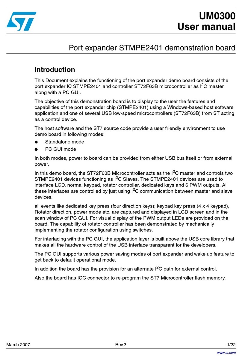
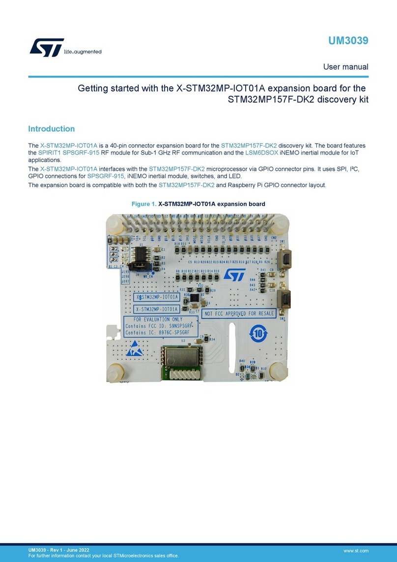
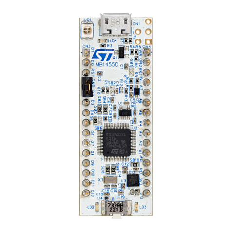
ST STM32MP157D-DK1 User manual

Introduction
The STM32MP157D-DK1 and STM32MP157F-DK2 Discovery kits (STM32MP157x-DKx) are designed as complete
demonstration and development platforms for STMicroelectronics Arm®-based dual Cortex®-A7 32 bits and Cortex®-M4 32
bits MPUs in the STM32MP1 Series and their STPMIC1 companion chip. They leverage the capabilities increased-frequency
800 MHz of STM32MP1 Series microprocessors to allow users to develop applications using STM32 MPU OpenSTLinux
Distribution software (such as STM32MP1Starter) for the main processor and STM32CubeMP1 software for the co-processor.
They feature 16-bit DDR3L 4 Gbits at 533 MHz, MIPI DSISM 2 lanes at 1 Gbps, USB Type-C® DRP HS port, USB Type-A Host
HS ports, audio codec with analog audio input / output, microSD™ card high-speed mode up to 50 MHz, Gigabit Ethernet,
HDMI® up to 720p60 (1280 × 720), 40-pin extended GPIOs, ARDUINO®, Wi‑Fi® 802.11b/g/n, Bluetooth® Low Energy 4.1, and
ST-LINK/V2-1 (UART console).
The STM32MP157F-DK2, shown with display removed in Figure 1 and Figure 2, is used as a reference design for user
application development. It cannot be considered as the hardware design of a final application.
The hardware features of the Discovery kits are available for users to develop their applications: USB, Ethernet, LTDC, TFT
LCD MIPI DSISM, microSD™ card, audio codec, user buttons, Wi‑Fi®, and Bluetooth® Low Energy. Extension headers allow easy
connection of an ARDUINO® board for a specific application.
An ST-LINK/V2-1 is integrated on the board, as embedded in-circuit debugger and programmer for the STM32 MPU and the
USB Virtual COM port bridge.
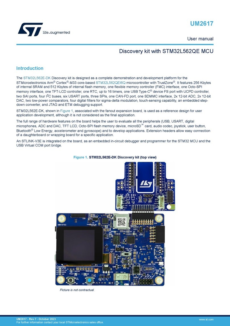
Figure 1. STM32MP157F-DK2 top view Figure 2. STM32MP157F-DK2 bottom view
Pictures are not contractual.
Discovery kits with increased-frequency 800 MHz STM32MP157 MPUs
UM2637
User manual
UM2637 - Rev 2 - January 2022
For further information contact your local STMicroelectronics sales office.
www.st.com

1Features
• Common features
– STM32MP157 Arm®-based dual Cortex®‑A7 800 MHz 32 bits + Cortex®‑M4 32 bits MPU in TFBGA361
package
– ST PMIC STPMIC1
– 4-Gbit DDR3L, 16 bits, 533 MHz
– 1-Gbps Ethernet (RGMII) compliant with IEEE-802.3ab
– USB OTG HS
– Audio codec
– 4 user LEDs
– 2 user and reset push-buttons, 1 wake-up button
–5 V / 3 A USB Type-C® power supply input (not provided)
– Board connectors:
◦ Ethernet RJ45
◦ 4 × USB Host Type-A
◦USB Type-C® DRP
◦MIPI DSISM
◦ HDMI®
◦ Stereo headset jack including analog microphone input
◦ microSD™ card
◦ GPIO expansion connector (Raspberry Pi® shield capability)
◦ ARDUINO® Uno V3 expansion connectors
– On-board ST-LINK/V2-1 debugger/programmer with USB re-enumeration capability: Virtual COM port
and debug port
–STM32CubeMP1 and full mainline open-source Linux® STM32 MPU OpenSTLinux Distribution (such
as STM32MP1Starter) software and examples
– Support of a wide choice of Integrated Development Environments (IDEs) including IAR Embedded
Workbench®, MDK-ARM, and STM32CubeIDE
• Board-specific features
– 4" TFT 480×800 pixels with LED backlight, MIPI DSISM interface, and capacitive touch panel
– Wi‑Fi® 802.11b/g/n
– Bluetooth® Low Energy 4.1
Note: Arm is a registered trademark of Arm Limited (or its subsidiaries) in the US and/or elsewhere.
UM2637
Features
UM2637 - Rev 2 page 2/47

2Ordering information
To order an STM32MP157 Discovery kit, refer to Table 1. Additional information is available from the datasheet
and reference manual of the target STM32.
Table 1. List of available products
Order code Board reference Target STM32 Differentiating feature
STM32MP157D-DK1 • MB1272 STM32MP157DAC1 • Basic security
STM32MP157F-DK2 • MB1272
• MB1407(1) STM32MP157FAC1
• Secure Boot and cryptography
• LCD
• Wi‑Fi®
• Bluetooth® Low Energy
1. LCD extension board.
2.1 Codification
The meaning of the codification is explained in Table 2.
Table 2. Codification explanation
STM32MP1XXY-DKZ Description Example: STM32MP157F-DK2
STM32MP1 MPU series in STM32 Arm Cortex MPUs STM32MP1 Series
XX MPU product line in the series STM32MP157
Y
Options:
• D: basic security, 800 MHz increased frequency
• F: Secure Boot, cryptography hardware, 800 MHz
increased frequency
Secure Boot, cryptography hardware,
800 MHz increased frequency
DKZ
Discovery kit configuration:
• DK1: basic
• DK2: LCD, Wi‑Fi®, and Bluetooth® Low Energy
LCD, Wi‑Fi®, and Bluetooth® Low
Energy
UM2637
Ordering information
UM2637 - Rev 2 page 3/47

3Development environment
3.1 System requirements
• Multi‑OS support: Windows® 10, Linux® 64-bit, or macOS®
• USB Type-C® to USB Type-C® charger 5 V / 3 A
• USB Type-C® to Type-A cable
• USB Type-A or USB Type-C® to Micro-B cable
Note: macOS® is a trademark of Apple Inc., registered in the U.S. and other countries and regions.
Linux® is a registered trademark of Linus Torvalds.
All other trademarks are the property of their respective owners.
3.2 Development toolchains
• IAR Systems® - IAR Embedded Workbench®(1)
• Keil® - MDK-ARM(1)
• STMicroelectronics - STM32CubeIDE
• GCC
1. On Windows® only.
3.3 Demonstration software
The STM32 MPU OpenSTLinux Distribution and STM32CubeMP1 base demonstration software is preloaded in
the microSD™ for easy demonstration of the device peripherals in standalone mode. The latest versions of the
demonstration source code and associated documentation can be downloaded from www.st.com.
UM2637
Development environment
UM2637 - Rev 2 page 4/47

4Conventions
Table 3 provides the conventions used for the ON and OFF settings in the present document.
Table 3. ON/OFF convention
Convention Definition
Jumper JPx ON Jumper fitted
Jumper JPx OFF Jumper not fitted
Jumper JPx [1-2] Jumper fitted between Pin 1 and Pin 2
Solder bridge SBx ON SBx connections closed by 0 Ω resistor
Solder bridge SBx OFF SBx connections left open
Resistor Rx ON Resistor soldered
Resistor Rx OFF Resistor not soldered
Capacitor Cx ON Capacitor soldered
Capacitor Cx OFF Capacitor not soldered
UM2637
Conventions
UM2637 - Rev 2 page 5/47

5Delivery recommendations
Before first use, check the board for any damage that might have occurred during shipment, that all socketed
components are firmly fixed in their sockets and that none are loose in the plastic bag.
UM2637
Delivery recommendations
UM2637 - Rev 2 page 6/47

6Hardware layout and configuration
Figure 3. STM32MP157x-DKx hardware block diagram
STM32MP157x
RTC
SWD
32 KHz crystal
ST-LINK/V2-1
USB
Capacitive touch
panel multi points
USB Type- C® USB
DRP
LCD TFT
4" 480 x 800
USB
Host
USB Hub
UART
ARDUINO® Uno
connectors
GPIOs
Bluetooth® Low
Energy V4.1
UART
microSD™ card
connector SDMMC
HSI
I2C1
GPIO User interface
4x LEDs
User interface
RESET buttons
GPIO
SAI Audio DAC &
amplifier Stereo jack
line out / Mic_IN
STPMIC1
5V_VIN
Type-C® / Type-C®
cable
24 MHz crystal
I2C1
I2C1
GPIO 40-pin
connector
GPIOs
Wi-Fi® 802.11 b/g/n
SDMMC
DDR3L DDR
LTDC HDMI®
RGMII Ethernet
DSI
I2C4
I2C4
I2C1
I2C4
Power supply
Feature not available on STM32MP157D-DK1
UM2637
Hardware layout and configuration
UM2637 - Rev 2 page 7/47

Figure 4. STM32MP157x-DKx PCB layout: top side
Ethernet connector
(CN8)
Power in 5 V
(CN6)
Ethernet PHY
(U18)
Power in LED
(LD2)
Wi-Fi® / Bluetooth® Low Energy
(U8)
DSISM connector (CN4)
VBAT connector (CN3)
STPMIC (U4)
40-pin connector (CN2)
USB Hub (U7)
DDR3L (U5)
USB Host
(CN1)
HDMI® bridge (U14)
STM32MP157 (U13)
USB Host
(CN5)
USB Type-C®
(CN7)
HDMI®
(CN9)
STUSB1600 (U12)
Wake-up button (B1)
Reset button (B2)
User1 button (B3)
User2 button (B4)
Audio connector (CN10)
User LED (LD5)
User LED (LD6)
User LEDs (LD7, LD8)
STLK LED (LD4)
ST-LINK USB (CN11)
ST-LINK STM32 (U19)
UM2637
Hardware layout and configuration
UM2637 - Rev 2 page 8/47

Figure 5. STM32MP157x-DKx PCB layout: bottom side
ARDUINO® connector
(CN13)
ARDUINO® connector
(CN14)
microSD™ card
(CN15)
ARDUINO® connector
(CN16)
ARDUINO® connector
(CN17)
BOOT mode
(SW1)
6.1 Embedded ST-LINK/V2-1
6.1.1 Description
To debug the on-board STM32 MPU, the ST-LINK/V2-1 programming and debugging tool is integrated in the
STM32MP157x-DKx Discovery kit. The embedded ST-LINK/V2-1 supports only SWD and VCP for STM32
devices. For information about the debugging and programming features of ST-LINK/V2-1, refer to the ST-
LINK/V2 in-circuit debugger/programmer for STM8 and STM32 user manual (UM1075) and Overview of ST-LINK
derivatives technical note (TN1235). It is recommended to power the board (5V_VIN) before plugging the USB
debug cable to the Micro-B connector.
Figure 6. CN11 ST-LINK USB Micro-B connector pinout
UM2637
Embedded ST-LINK/V2-1
UM2637 - Rev 2 page 9/47

Table 4. CN11 ST-LINK USB Micro-B connector pinout
Pin Pin name Signal name ST-LINK STM32 pin Function
1 VBUS 5V_USB_ST_LINK - VBUS Power
2 DM USB_STLK_N PA11 DM
3 DP USB_STLK_P PA12 DP
4 ID - GND ID
5 GND GND GND GND
6.1.2 Drivers
Before connecting STM32MP157x-DKx to a Windows® (7, 8, or 10) PC via the USB, a driver for ST-LINK/V2-1
must be installed (not required for Windows® 10). It is available from the www.st.com website.
In cases where the STM32MP157x-DKx Discovery kit is connected to the PC before the driver is installed, some
Discovery kit interfaces may be declared as “Unknown” in the PC device manager. In this case, the user must
install the dedicated driver files, and update the driver of the connected device from the device manager.
6.1.3 ST-LINK/V2-1 firmware upgrade
The ST-LINK/V2-1 embeds a firmware upgrade mechanism for in-situ upgrade through the USB port. As firmware
may evolve during the lifetime of the ST-LINK/V2-1 product (addition of new functionalities, bug fixes, or support
of new microprocessor families), visiting the www.st.com website is recommended before starting to use the
STM32MP157x-DKx Discovery kit, then periodically to stay up-to-date with the latest firmware version.
6.2 Power supply
6.2.1 5 V power supply
The STM32MP157x-DKx Discovery kit is designed to be powered by a 5 V DC power source at 3 A maximum
such as:
• 5V_VBUS connected to the CN6 connector through a USB Type-C® to USB Type-C® cable
The two lines USB_PWR_CC1 and USB_PWR_CC2 are connected to PA4 and PA5 respectively to check
what is connected to CN6 and control features enabling:
– Legacy cable
– Personal computer
– 5 V DC power source at 3 A
Depending on the current needed on the devices connected to the USB port, and the board itself, power
limitations can prevent the system from working as expected. The user must ensure that the STM32MP157x-DKx
Discovery kit is supplied with the correct power source depending on the current needed. It is recommended to
use a USB Type-C® to USB Type-C® 5 V/3 A charger.
6.2.2 STPMIC1 power supply
For general information concerning the STPMIC1, refer to the datasheet on the www.st.com website.
STPMIC1 supply
• VDD_CORE (BUCK1) used to supply the core of the STM32MP157x
– Value: 1.2 V
• VDD_DDR (BUCK2) used to supply the DDR core and I/Os
– Value: 1.35 V
• VDD (BUCK3) used to supply the VDDA and VDD domains of the STM32MP157x
– Value: 3.3 V
• 3V3 (BUCK4) used to provide the 3.3 V to the different features available on the Discovery kit
– Value: 3.3 V
UM2637
Power supply
UM2637 - Rev 2 page 10/47

• VREF_DDR used to supply the DDR reference voltage
– Value: 1.65 V
• VTT_DDR (LDO3) used to supply the termination resistors of the DDR
– Value: 1.65 V
• 1V8_Audio (LDO1) used to supply the digital/analog of the audio codec
– Value: 1.8 V
• 1V2_HDMI (LDO6) used to supply the digital core and analog part of the HDMI transceiver
– Value: 1.2 V
• 3V3_HDMI (LDO2) used to supply the I/Os of the HDMI transceiver
– Value: 3.3 V
• VDD_USB (LDO4) used to supply the USB phy of the STM32MP157x
– Value: 3.3 V
6.3 Clock sources
6.3.1 LSE clock references
The LSE clock references on the STM32MP157x microprocessor are provided by the external crystal X2:
• 32.768 kHz crystal from NDK: reference NX2012SA
6.3.2 HSE clock references
The HSE clock references on the STM32MP157x microprocessor are provided by the external crystal X6:
• 24 MHz crystal from NDK: reference NX2016SA
6.4 Reset sources
The reset signal of STM32MP157x-DKx is active low. The internal PU forces the RST signal to a high level.
The sources of reset are:
• Reset button B2 (black button)
• STPMIC1
• Embedded ST-LINK/V2-1
• ARDUINO® connector CN16: pin 3, reset from the ARDUINO® board
• STM32MP157x
6.5 Boot mode
6.5.1 Description
At startup, the boot source used by the internal bootROM is selected by the Boot pins. Table 5 describes the
configurations of the Boot pins.
Table 5. Boot mode pins
Boot 0 Boot 1(1) Boot 2 Boot mode
0 0 0 Forced USB boot for flashing.
1 0 0 Not supported.
0 0 1 Engineering boot.
1 0 1 SD card on SDMMC1.
1. Pin Boot 1 is always tied to "0" by a pull-down resistor.
UM2637
Clock sources
UM2637 - Rev 2 page 11/47

Figure 7 shows the configurations of the boot-related switch SW1.
Figure 7. Boot-mode switch SW1
Forced USB boot
for flashing Engineering boot Boot from SD card
6.6 Audio
6.6.1 Description
The audio codec is connected through an SAI interface to the STM32MP157x microcontroller. This component
supports the TDM feature of the SAI port. The TDM feature offers STM32MP157x the capability to stream stereo
audio channels.
6.6.2 Operating voltage
The audio codec has two power supplies:
• VL, connected to the 3.3 V provided by the STPMIC1
• 1V8_AUDIO, dedicated 1.8 V source provided by the STPMIC1
6.6.3 Audio codec interface
Audio codec interfacing is performed through the SAI2 and I2C1 interfaces of the STM32MP157x.
Table 6 describes the I/O configuration of the audio codec interface.
Table 6. I/O configuration for the audio interface
I/O Configuration
PG9 PG9 used as AUDIO RESETN (active LOW)
PE0 PE0 used as SAI2_MCLKA
PF11 PF11 used as SAI2_SDB shared with GPIO expansion
PI7 PI7 used as SAI2_FSA shared with GPIO expansion
PI5 PI5 used as SAI2_SCKA shared with GPIO expansion
PI6 PI6 used as SAI2_SDA shared with GPIO expansion
PD12 PD12 used as I2C1_SCL shared between USB, DSI, HDMI
PF15 PF15 used as I2C1_SDA shared between USB, DSI, HDMI
UM2637
Audio
UM2637 - Rev 2 page 12/47

6.6.4 Headphone outputs
The STM32MP157D-DK1 and STM32MP157F-DK2 Discovery kits can drive a stereo headphone. The
STM32MP157x sends the stereo audio channels to the codec via its SAI2 TDM port. The codec converts the
digital audio stream to stereo analog signals. It then boosts them for direct drive of the headphone connected to
the CN10 3.5 mm stereo jack receptacles on the board.
The audio codec is set by an I2C bus. The address is a 7 bit address plus one bit for read/write (high for read, low
for write). The AD0 pin, connected to GND, gives the least-significant address bit. The address of the audio codec
is 0b1001010x: 0x94 to write and 0x95 to read.
6.6.5 Audio jack connector
Figure 8 shows the CN10 audio jack connector pinout.
Figure 8. CN10 audio jack connector pinout
Table 7 describes the CN10 audio jack connector pinout.
Table 7. CN10 audio jack connector pinout
Pin Pin name Signal name Codec pin Function
1 1 MIC_IN MICIN1 Microphone IN
2 2 GND GND GND
3 3 AOUTB AOUTB OUT_SPEAKER_RIGHT
4 4 AOUTA AOUTA OUT_SPEAKER_LEFT
6.6.6 I/O restriction
SAI2 is shared between the audio codec and the GPIO expansion connector. By default, the audio codec is
available because of solder bridges SB13, SB14, SB15, and SB16.
UM2637
Audio
UM2637 - Rev 2 page 13/47

6.7 USB Host
6.7.1 Description
The STM32MP157D-DK1 and STM32MP157F-DK2 Discovery kits provide four USB Host ports (dual-USB
sockets CN1 and CN5) through the use of the USB Hub, which has a full power management for each USB
port: no I/O is needed from the STM32MP157x.
6.7.2 USB Host interface
Table 8 describes the I/O configuration for the USB Host interface.
Table 8. I/O configuration for the USB Host interface
I/O Configuration
PD12 PD12 used as I2C1_SCL shared between AUDIO, DSI, and HDMI(1)
PF15 PF15 used as I2C1_SDA shared between AUDIO, DSI, and HDMI(1)
USB_DP1 USB1_P
USB_DM1 USB1_N
1. I2C1 not connected by default (SB7 and SB8 OFF).
Figure 9 shows the CN1 and CN5 USB Type-A connector pinout.
Figure 9. CN1 and CN5 USB Type-A connector pinout
Table 9 describes CN1 and CN5 USB Host connector pinout.
Table 9. CN1 and CN5 USB Host connector pinout
Pin Pin name Signal name Function
CN1
T1 T1 VBUS VBUS
T2 T2 USB1CN25_N DM
T3 T3 USB1CN25_P DP
T4 T4 GND GND
B1 B1 VBUS VBUS
B2 B2 USB1CN25_N DM
UM2637
USB Host
UM2637 - Rev 2 page 14/47

Pin Pin name Signal name Function
B3 B3 USB1CN25_P DP
B4 B4 GND GND
CN5
T1 T1 VBUS VBUS
T2 T2 USB1CN26_N DM
T3 T3 USB1CN26_P DP
T4 T4 GND GND
B1 B1 VBUS VBUS
B2 B2 USB1CN26_N DM
B3 B3 USB1CN26_P DP
B4 B4 GND GND
6.8 USB Type-C® HS
6.8.1 Description
The STM32MP157D-DK1 and STM32MP157F-DK2 Discovery kits support USB high-speed (HS) communication.
USB connector CN7 is a USB Type-C® connector.
The STM32MP157D-DK1 and STM32MP157F-DK2 Discovery kits support the USB Type-C® Source mode.
6.8.2 Operating voltage
The STM32MP157D-DK1 and STM32MP157F-DK2 Discovery kits support 5 V USB voltage from 4.75 V to
5.25 V.
6.8.3 USB HS Source
When a USB Device connection to the CN7 USB Type-C® connector of STM32MP157D-DK1 or STM32MP157F-
DK2 is detected, the Discovery kit starts behaving as a USB Host.
6.8.4 USB Type-C® connector
Figure 10 shows the pinout of USB Type-C® connector CN7.
Figure 10. CN7 USB Type-C® connector pinout
GND TX1+ TX1- VBUS CC1 D+ D- SBU1 VBUS RX2- RX2+ GND
GND RX1+ RX1- VBUS SBU2 D- D+ CC2 VBUS TX2- TX2+ GND
B12 B11 B10 B9 B8 B7 B6 B5 B4 B3 B2 B1
A1 A2 A3 A4 A5 A6 A7 A8 A9 A10 A11 A12
UM2637
USB Type-C® HS
UM2637 - Rev 2 page 15/47

Table 10 describes the pinout of USB Type-C® connector CN7.
Table 10. CN7 USB Type-C® connector pinout
Function STM32 pin Signal name Pin
name Pin Pin Pin
name Signal name STM32 pin Function
GND - GND GND A1 B12 GND GND - GND
TX1+ - - TX1+ A2 B11 RX1+ - - RX1+
TX1- - - TX1- A3 B10 RX1- - - RX1-
VBUS - - VBUS A4 B9 VBUS - - VBUS
CC1 - - CC1 A5 B8 SBU2 - - SBU2
D+ USB_DP2 USB_DP2 D+ A6 B7 D- USB_DM2 USB_DM2 D-
D- USB_DM2 USB_DM2 D- A7 B6 D+ USB_DP2 USB_DP2 D+
SBU1 - - SBU1 A8 B5 CC2 - - CC2
VBUS - - VBUS A9 B4 VBUS - - VBUS
RX2- - - RX2- A10 B3 TX2- - - TX2-
RX2+ - - RX2+ A11 B2 TX2+ - - TX2+
GND - GND GND A12 B1 GND GND - GND
6.9 microSD™ card
6.9.1 Description
The CN15 slot for the microSD™ card is routed to STM32MP157x SDIO port (SDMMC1). This interface is
compliant with SD Memory Card Specification Version 3.01: SDR50.
6.9.2 Operating voltage
The microSD™ card interface is only compatible with the 3.3 V voltage range: from 2.7 V to 3.6 V. All microSD™
card types are supported (including SDHC and SDXC), but only Default and High-Speed modes (3 V) are
supported on STM32MP157D-DK1 and STM32MP157F-DK2. UHS-I modes (1.8 V) are not supported on these
Discovery kits.
6.9.3 microSD™ card interface
The microSD™ card interface is used in the four data lines D[0:3] with one clock (CLK), one command line (CMD),
and one card detection signal (CARD_DETECT).
The SDMMC1 is a bootable interface.
Table 11 describes the I/O configuration for the SDIO interface.
Table 11. I/O configuration for the SDIO interface
I/O Configuation
PB7 PB7 is connected to µSD_DETECT
PC8 PC8 is connected to SDMMC1_D0
PC9 PC9 is connected to SDMMC1_D1
PC10 PC10 is connected to SDMMC1_D2
PC11 PC11 is connected to SDMMC1_D3
PC12 PC12 is connected to SDMMC1_CLK
PD2 PD2 is connected to SDMMC1_CMD
UM2637
microSD™ card
UM2637 - Rev 2 page 16/47

Figure 11 shows the pinout of the microSD™ connector CN15.
Figure 11. microSD™ card connector CN15
Table 12 describes pinout of the microSD™ connector CN15.
Table 12. CN15 microSD™ connector pinout
Pin Pin name Signal name STM32 pin Function
1 DAT2 SDMMC1_D2 PC10 SDIO.D2
2 DAT3_CD SDMMC1_D3 PC11 SDIO.D3
3 CMD SDMMC1_CMD PD2 SDIO.CMD
4 3V3 3V3 - VDD_SDCARD
5 CLK SDMMC1_CLK PC12 SDIO.CLK
6 VSS GND - GND
7 DAT0 SDMMC1_D0 PC8 SDIO.D0
8 DAT1 SDMMC1_D1 PC9 SDIO.D1
9 GND GND - GND
10 CARD_DETECT uSD_DETECT PB7 SDCARD_DETECT active LOW
6.10 LEDs
6.10.1 Description
The LD2 LED turns green when the power cable is inserted in connector CN6.
Two general-purpose color LEDs (LD7 and LD8) are available as light indicators:
• The LD7 orange LED is used as STM32Cube examples verdict LED.
• The LD8 blue LED is used as Linux® Heartbeat LED, which is blinking as long as Linux® is alive on the
Cortex®-A.
The two user LEDs, the green LD5 and orange LD6 LEDs, are directly connected to the STM32MP157x.
UM2637
LEDs
UM2637 - Rev 2 page 17/47

6.10.2 Operating voltage
All LEDs are driven by the I/O level; they are operating in the 3.3 V voltage range.
6.10.3 LED interface
Table 13 describes the I/O configuration of the LED interface.
Table 13. I/O configuration of the LED interfaces
I/O Configuration
PA14 PA14 is connected to the green LED LD4. Active Low.
PA13 PA13 is connected to the red LED LD6. Active Low.
PH7 PH7 is connected to the orange LED LD7. Active High.
PD11 PD11 is connected to the blue LED LD8. Active High.
6.11 Buttons
6.11.1 Description
The STM32MP157D-DK1 and STM32MP157F-DK2 Discovery kits provide four types of buttons:
• Wake-up button (B1)
– Allows the platform to be woken up from any low-power mode
– Connected to STPMIC1 PONKEY, which generates a wake up signal on STM32MP157x PA0
• Reset button (B2)
– Used to reset the Discovery kit
• USER1 button (B3)
– Used at boot time by U-Boot to enter the USB programming mode
• USER2 button (B4)
–Used at boot time by U-Boot to enter the Android® Fastboot mode
6.11.2 I/O interface
Table 14 describes the I/O configuration for the physical user interface.
Table 14. I/O configuration for the physical user interface
I/O Configuration
NRST Reset button (B2). Active Low.
- Wake-up button (B1). Connected to the PONKEYn pin of the STPMIC1
PA13 USER2 user button (B4)
PA14 USER1 user button (B3)
6.12 HDMI®
6.12.1 Description
The STM32MP157D-DK1 and STM32MP157F-DK2 Discovery kits offer an HDMI® connection for a TV monitor
through the use of an HDMI® transmitter.
The resolution is up to 720p60 (1280 × 720).
UM2637
Buttons
UM2637 - Rev 2 page 18/47

Input signals are 24 bits digital RGB (LTDC) for the video and I2S2 for the audio. Refer to the STM32MP157x
datasheet for details.
The control signals are I2C1, one interruption, and a dedicated reset.
The Consumer Electronic Control (CEC) is also available through the HDMI® transmitter (transmitter bypassed).
6.12.2 HDMI® I/O interface
Table 15 describes the I/O configuration for the HDMI® interface.
Table 15. I/O configuration for the HDMI® interface
I/O Configuration
PB6 PB6 is connected to HDMI_CEC.
PD9 PD9 is connected to LTDC_B0.
PG12 PG12 is connected to LTDC_B1.
PG10 PG10 is connected to LTDC_B2.
PD10 PD10 is connected to LTDC_B3.
PI4 PI4 is connected to LTDC_B4.
PA3 PA3 is connected to LTDC_B5.
PB8 PB8 is connected to LTDC_B6.
PD8 PD8 is connected to LTDC_B7.
PE5 PE5 is connected to LTDC_G0.
PE6 PE6 is connected to LTDC_G1.
PH13 PH13 is connected to LTDC_G2.
PH14 PH14 is connected to LTDC_G3.
PH15 PH15 is connected to LTDC_G4.
PI0 PI0 is connected to LTDC_G5.
PI1 PI1 is connected to LTDC_G6.
PI2 PI2 is connected to LTDC_G7.
PH2 PH2 is connected to LTDC_R0.
PH3 PH3 is connected to LTDC_R1.
PH8 PH8 is connected to LTDC_R2.
PH9 PH9 is connected to LTDC_R3.
PH10 PH10 is connected to LTDC_R4.
PC0 PC0 is connected to LTDC_R5.
PH12 PH12 is connected to LTDC_R6.
PE15 PE15 is connected to LTDC_R7.
PG7 PG7 is connected to LTDC_CLK.
PF10 PF10 is connected to LTDC_DE.
PI10 PI10 is connected to LTDC_HSYNC.
PI9 PI9 is connected to LTDC_VSYNC.
PA9 PA9 is connected to I2S2_CK.
PB9 PB9 is connected to I2S2_WS.
PI3 PI3 is connected to I2S2_SDO.
PG1 PG1 is connected to HDMI_INT.
UM2637
HDMI®
UM2637 - Rev 2 page 19/47

I/O Configuration
PD12 PD12 is connected to I2C1_SCL (I2C shared).
PF15 PF15 is connected to I2C1_SDA (I2C shared).
PA10 PA10 is connected to HDMI_NRST
Figure 12 shows the pinout of HDMI® connector CN9.
Figure 12. CN9 HDMI® connector pinout
Table 16 describes the pinout of HDMI® connector CN9.
Table 16. CN9 HDMI® connector pinout
Pin Pin name Signal name
1 RX2+ TX2C_P
2 GND GND
3 RX2- TX2C_N
4 TX1+ TX1C_P
5 GND GND
6 RX1- TX1C_N
7 RX0+ TX0C_P
8 GND GND
9 RX0- TX0C_N
10 RXC+ TXCC_P
11 GND GND
12 RXC- TXCC_N
13 CEC CEC_A
14 - -
15 SCL DSCL
16 SDA DSDA
17 GND GND
UM2637
HDMI®
UM2637 - Rev 2 page 20/47
This manual suits for next models
2
Table of contents
Other ST Computer Hardware manuals

ST
ST FP-SNS-FLIGHT1 User manual

ST
ST X-NUCLEO-53L3A2 User manual

ST
ST X-NUCLEO-GFX02Z1 User manual

ST
ST STDES-PFCBIDIR User manual

ST
ST STM32F078CB User manual

ST
ST STM32F101 series User manual

ST
ST AEK-LCD-DT028V1 User manual

ST
ST X-NUCLEO-IHM08M1 User manual

ST
ST X-NUCLEO-OUT13A1 User manual

ST
ST EVLKST8500GH-2 User manual

ST
ST X-NUCLEO-6283A1 User manual

ST
ST X-NUCLEO-S2915A1 User manual

ST
ST I-CUBE-LRWAN User manual

ST
ST STM32L562E-DK User manual

ST
ST TIP122FP User manual

ST
ST STM32WL Series User manual

ST
ST STEVAL-CCH002V1 User manual

ST
ST X-NUCLEO-S2868A2 User manual

ST
ST STM32G0 User manual

ST
ST STEVAL-ISF001V2 User manual