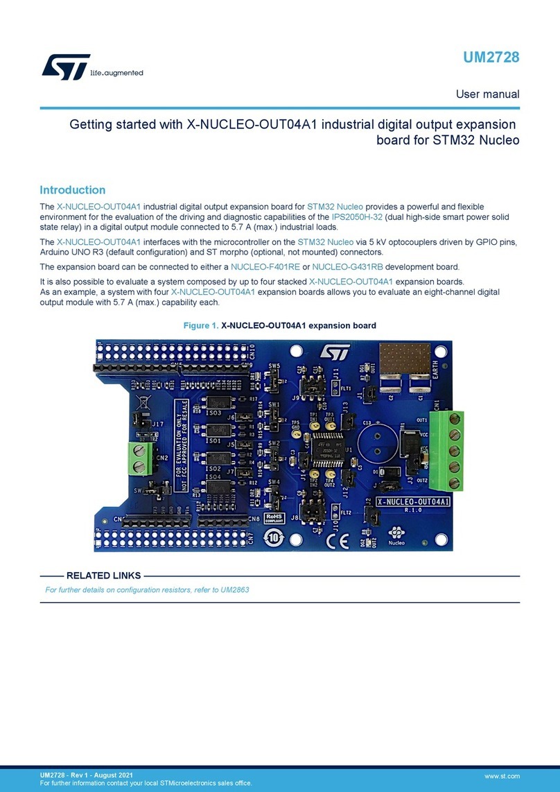
ST STEVAL-SCR002V1 User manual

Introduction
Improvement of power density and reliability is a major trend for power supply manufacturers. Moving from passives and
mechanical parts to silicon devices considerably contributes to this progress.
During the startup of an AC-DC power converter, the high current due to the charge of the DC bulk capacitor can rise up to 10
times the nominal steady state current of the system. This inrush current induces a voltage drop on the AC mains that might
affect the operation of other equipment connected to the same power network.
The inrush triggers or damages the serial devices, such as the circuit breaker, the wire fuse, the capacitor, or the bridge rectifier.
To preserve the safety of the electrical installation and the reliability of the power converter, it is necessary to limit this inrush
current.
The STEVAL-SCR002V1 evaluation board introduces a simple and innovative AC-DC front-end circuit. The bridge rectifier
consists of diodes and silicon-controlled rectifiers (SCRs) that are implemented in the bridge low side.
An uninsulated power supply and a few SMD discrete components make the design very compact. The board can be easily
implemented on existing PFC or fly-back converters for plug-and-play tests. The solution, based on the high temperature
TN1605H-6T SCRs, totally replaces front-end electro-mechanical relays, bypassing the inrush current-limiting resistor.
Figure 1. STEVAL-SCR002V1 evaluation board
Getting started with the STEVAL-SCR002V1 SCR based inrush current limiter
board with non-isolated gate driver
UM2948
User manual
UM2948 - Rev 1 - July 2022
For further information contact your local STMicroelectronics sales office. www.st.com

1Getting started
1.1 Safety precautions
Danger: Use the STEVAL-SCR002V1 board only after applying a fire-resistant cover. The cover is
not included in the board package.
There is danger of serious personal injury, property damage or death due to electrical shock
and burn hazards if the kit or components are improperly used or installed incorrectly.
Warning: The kit is not electrically isolated from the high-voltage supply AC-DC input.
The evaluation board is directly linked to the mains voltage. No insulation is ensured
between the accessible parts and the high voltage. All measurement equipment must be
isolated from the mains before powering the board.
When using an oscilloscope with the evaluation board, it must be isolated from the AC line.
This prevents shock from occurring as a result of touching any single point in the circuit, but
does NOT prevent shock when touching two or more points in the circuit.
Caution: During assembly, testing, and operation, the evaluation board poses several inherent hazards, including bare
wires, moving or rotating parts and hot surfaces. All operations involving transportation, installation, use and
maintenance must be performed by skilled technical personnel who is familiar with the installation, use and
maintenance of power electronic systems.
The board has to be connected directly on the mains. Non-isolated parts at high-voltage levels are present on
both sides of the PCB.
The high current flowing through the two SCRs generates heat: the board temperature can reach up to 150°C
at full power. Be aware that, due to thermal inertia, the board could remain hot even after current has ceased to
flow.
Work area safety:
The work area must be clean and tidy.
Do not work alone when boards are powered.
Protect the area against any unauthorized access by putting suitable barriers and signs.
A system architecture that supplies power to the evaluation board must be equipped with additional control
and protective devices in accordance with the applicable safety requirements (i.e., compliance with technical
equipment and accident prevention rules).
Electrical safety:
Remove the power supply from the evaluation board and electrical loads before performing any electrical
measurement. Arrange measurement setup, wiring, and configuration, paying attention to the high voltage
section. Once the setup is complete, power the board. Fuse protection is not included with this evaluation board.
Danger: Do not touch the evaluation board when it is powered or immediately after it has been
disconnected from the voltage supply as several parts and power terminals containing
potentially energized capacitors need time to discharge, and heat-sinks and transformers
may still be very hot.
UM2948
Getting started
UM2948 - Rev 1 page 2/28

Personal safety:
Always wear suitable personal protective equipment, such as insulating gloves and safety glasses.
Take adequate precautions and install the board preventing accidental touch.
Use protective shields, such as insulating box with interlocks.
1.2 Features
• Two TN1605H-6T 16 A - 600 V Hi Tj SCRs in a TO-220 package, used to bypass the inrush resistor
• Compact solution: 43.6 x 28.5 mm (≈ 1.8 sq in)
• Compatible with AC-DC converters with or without PFC in all modes: CCM, CRM, and DCM
• Enable signal (EN = 3.3 V to 15 V) versus GND_DC (DC or PWM signal)
• Suitable for applications from 50 W up to 1000 W (230 VRMS, TAMB = 60°C)
• Compliant with AC or DC input voltage: 90-265 VAC, 50/60 Hz, or 120-400 VDC
• Robust, immune (2 kV IEC 61000-4-5, 4 kV IEC 61000-4-4)
• Low EMI noise (EN55014 and EN55022) solution
1.3 Circuit and purpose
The STEVAL-SCR002V1 purpose is to bypass the NTC via the SCRs. The SCR driver consists of a triac and two
diodes.
At system startup, inrush current is limited by the NTC (see Section 3.1 ). When the DC capacitor is fully
charged, the MCU turns the SCR driver on to bypass the NTC (see Section 3.2 ).
Thanks to the innovative arrangement of the SCR gate driver components, only the positive biased SCR is on.
Therefore:
• no AC line polarity sensing is required;
• there is no SCR reverse loss;
• a single MCU pin can drive both SCRs.
SCRs gate driver Enable pin (EN) can be supplied by a DC, pulsed signal, or PWM signal to reduce consumption.
Both SCRs are more compact than a relay commonly used to bypass NTC.
The STEVAL-SCR002V1 evaluation board is designed and tested for 1 kW power. Higher power applications can
be easily achieved by choosing higher power SCRs and heatsink.
UM2948
Features
UM2948 - Rev 1 page 3/28

2Connection and startup
The figures below show the circuit diagram and the physical position of the components on the board.
Figure 2. STEVAL-SCR002V1: circuit simplified schematic
Figure 3. STEVAL-SCR002V1 components
STEVAL-SCR002V1 pinout:
•EN: enable pin. The NTC is bypassed as long as the enable pin is supplied with a positive voltage (from 3.3
to 15 V)
•GND_DC: DC voltage reference
•LINE: AC line voltage
•NEUTRAL: AC neutral voltage
•DC+: DC high voltage
The following figure shows a connection example of the STEVAL-SCR002V1 to a standard PFC with inrush
managed via relay.
UM2948
Connection and startup
UM2948 - Rev 1 page 4/28

Figure 4. Connection example of the STEVAL-SCR002V1 to a boost converter (PFC) - relay replacement
UM2948
Connection and startup
UM2948 - Rev 1 page 5/28

3Operation
The most common solution to limit the inrush current at startup is to use a serial impedance after the rectifier
bridge. To reduce the power loss, a mechanical relay bypasses the serial impedance as soon as the output DC
capacitor is charged and when the converter starts up.
The figure below shows the typical schematic of a power converter using a bypass relay at the DC bus high side
(NTC upstream) and at the DC bus low side (NTC downstream).
Figure 5. Typical schematic of a power converter using relay bypass
The bulkiness of the relay and its slow response has led to a new architecture based on a half-controlled rectifier
bridge.
The STEVAL-SCR002V1 board allows replacing the relay with two SCRs triggered by Q1 (Z0110MN, SOT223
package, four-quadrant triac), offering high reliability, long service lifetime, electromagnetic interference reduction
and a faster response to line dips. Moreover, this bypass solid-state solution has no moving parts, preventing from
spark and contact arcing that are the root cause of the reduction of the electromechanical relay lifetime.
Solid-state topologies with SCRs allow applications to comply easily with the following standards:
• IEC61000-3-3 (voltage fluctuations and flicker in public low-voltage supply systems, for equipment with rated
current ≤ 16 A);
• IEC61000-4-11 (voltage dips, short interruptions, and immunity tests for voltage variations).
Figure 6. Schematic of the STEVAL-SCR002V1 connected to PFC
3.1 Startup
At system power-up, the EN signal is disabled and no gate current is applied to the Q1 gate terminal. Then, the
triac remains off and no current can flow through the SCR gates. As a result, SCRs X1 and X2 are in the off state.
The inrush current flows through the bridge diodes of the font-end rectifier, limited by the inrush power resistor
(NTC or PTC) as shown below.
UM2948
Operation
UM2948 - Rev 1 page 6/28

Figure 7. Startup phase - PFC bulk capacitor precharge (EN = 0 V)
During the positive half sine wave, the current flows through D3, boost inductor and diode, NTC, and D6.
During the negative half sine wave, the current flows through D4, boost inductor and diode, NTC, and D5.
With EN = 0 V, inrush current is limited by the NTC.
3.2 Steady state
As soon as the bulk capacitor of the PFC is charged, the PFC converter turns on. Then, the enable signal (for
instance, 5 V DC, or PWM 10 kHz α = 10%) is applied to the gate of the Q1 triac (Z0110MN). Q1 turns on. The
SCR gate currents flow through D1 and D2, according to the AC line polarity. TN1605H-6T X1 or X2 turns on and
off alternately and automatically, according to the AC line polarity.
In nominal operation mode, the two top diodes of the rectifier bridge (D3 and D4) and the two SCRs (X1 and X2)
rectify the AC line: the inrush resistor is then bypassed.
Figure 8. Steady state - PFC on, bypass on
3.3 SCR gate driver with automatic switching operation
One issue of SCR bypass topology is the power loss in the two SCRs when they are reverse biased. During the
steady state, at each mains period, one SCR is closed and rectifies the AC line current. The other SCR is reverse
biased and blocked.
Supplying the gate of the nonconducting SCR leads to high leakage currents, which, associated with reverse high
voltage, brings reverse power losses.
UM2948
Steady state
UM2948 - Rev 1 page 7/28

Figure 9. Example of SCR leakage current (Tj = 125°C)
The evaluation board solution is low side bypass topology: the TN1605H-6T SCR gate driver is implemented with
Z0110MN and STTH110A connected in series to the SCR gates. This solution allows controlling only the SCR
positively biased without sensing the polarity of the AC line signal.
Assume the PFC output capacitor is already charged and the PFC is in normal operation. Consider the AC
positive half sine wave. Also consider that Q1 is on with 50 mA pulsed gate current, thanks to the EN 5 V PWM
signal (10 kHz, α = 0.1, for instance). Thus, the positively biased SCR X1 is turned on. The nominal current flows
through the D3 diode, the PFC output stage, and X1.
During this AC positive half sine wave, D2 cathode to anode voltage is negative (VAK_D2 < 0), D2 diode is
blocked. No current can flow through the X2 gate and, consequently, the SCR X2 remains blocked as long as it is
reversed biased.
Thanks to the SCR gate driver topology, the nonconducting SCR gate cannot be supplied. In fact, its series diode
is blocked. Thus, no more reverse losses are added. D1 and D2 automatically switch the gate current to the
positively biased SCR. This explains why no polarity sense is required and no reverse conduction can occur.
Figure 10. SCR gate driver operation
UM2948
SCR gate driver with automatic switching operation
UM2948 - Rev 1 page 8/28

4Performance
To test the STEVAL-SCR002V1 performance, we used a standard 1500 W PSU. The PSU is rated at 93%
efficiency with 80% load power, with the schematic modified as shown in the figure below.
Figure 11. STEVAL-SCR002V1 performance test configuration
The original configuration, which uses a mechanical relay, has been replaced by connecting the STEVAL-
SCR002V1 low side SCR bypass solution.
4.1 Power efficiency
To perform the efficiency test, we used an electronic load from 10% to 100% of the total admissible power.
The figure below shows the results, which demonstrate the low side SCR bypass topology has no impact on the
total power losses and efficiency results. Thus, the SCR power losses, with their control circuits, have the same
power losses of the electro-mechanical relay, with its control coil consumption.
Figure 12. 1500 W PSU comparative efficiency test results (VAC = 230 V/50 Hz; Tamb = 25°C)
UM2948
Performance
UM2948 - Rev 1 page 9/28

4.2 Conducted EMI noise
The EN55014 standard defines the maximum levels of the conducted noise due to AC mains current switching.
The STEVAL-SCR002V1 evaluation board complies with the standard, as shown in the figure below.
No impact of the low-side SCR bypass topology compared to the original topology has been measured. The
results are identical.
Figure 13. EN55014 standard validation (average measurement) - VAC = 230 V/50 Hz, P = 1000 W
4.3 EMC immunity
We evaluated the immunity of the STEVAL-SCR002V1 subject to fast transient/bursts on the supply, according to
the test method described in the IEC 61000-4-4 standard.
Figure 14. Test schematic and waveform specification for IEC61000-4-4
We tested two couplings: one between line and ground, and one between neutral and ground. For each coupling,
we applied bursts to positive and negative polarities.
We achieved the same IEC61000-4-4 withstanding level with the original configuration using a relay and an NTC.
The low side bypass SCR solution has no impact on the burst immunity system performance.
Table 1. IEC61000-4-4 test results for the STEVAL-SCR002V1
Coupling Minimum level
Original
configuration
level
A class (1) B class (2)
A class (1) B class
(2)
A class
(1)
B class
(2)
L N L N
+ - + - + - + -
2.5 kV 3.8 kV 6 kV 2.5 kV >4 kV >4 kV >4 kV >4 kV 2.5 kV >4 kV 2.5 kV >4 kV
1. Normal operation within the limits specified by the manufacturer.
2. Temporary loss of function, degradation, or performance, which ceases when disturbance finishes. After this temporary loss,
the equipment under test recovers its normal performance without any operator’s intervention.
UM2948
Conducted EMI noise
UM2948 - Rev 1 page 10/28

4.4 Surge robustness
We performed the lightning surge robustness according to the IEC61000-4-5 test. We tested four configurations:
positive and negative surges with 90° and 0° phase angles as shown below.
Figure 15. IEC61000-4-5 surge test configuration
The EN pin is supplied with 5 V DC, the low side SCRs bypass the NTC, and the PFC output capacitor is already
charged through the NTC.
During the positive surge at the peak line voltage (A configuration), the SCR_N is already positively biased and
conducting. The surge current flows through the SCR_N.
Figure 16. Waveforms resulting from the 2 kV IEC61000-4-5 test (A configuration)
There are three phases for negative surge test results at the peak line voltage (B configuration):
• Phase 1: before the surge is applied, the nominal current flows through the SCR_N (positively biased).
• Phase 2: applying a negative surge, the AC main voltage VLN becomes negative and the SCR_N is
negatively biased. The SCR_N turns off and the SCR_L handles the surge current, becoming positively
biased. The TN1605H-6T is specified with an ITSM = 950 A for 30 µs pulse. The gate current is switched to
the positive biased SCR, thanks to the gate driver made of Z0110MN and STTH110A.
• Phase 3: when the lighting surge is completed, the VLN becomes positive again, the SCR_N is positively
biased and turns on. The SCR_L is reversed biased and turns off. The SCR_N handles the nominal current
and the system returns to its normal operation.
UM2948
Surge robustness
UM2948 - Rev 1 page 11/28

Figure 17. Waveforms resulting from the 2 kV IEC61000-4-5 test (B configuration)
The figure below shows how the positively biased SCR handles the surge current, during the surge test at 0°
phase angle.
Figure 18. Waveforms resulting from the 2 kV IEC61000-4-5 test (C and D configurations)
During the IEC 61000-4-5 lightning surge test, the triac, diodes, and SCR measured values are within the
specified values.
Components stay in a safe operating area during the 2 kV IEC61000-4-5 surge test.
UM2948
Surge robustness
UM2948 - Rev 1 page 12/28

5Thermal management
For a safe and reliable operation, it is important to keep the junction temperature of the SCR below its maximum
junction temperature. The STEVAL-SCR002V1 uses two high temperature TN1605H-6T SCRs that can operate at
up to 150°C.
To calculate the junction temperature, you need to know the ambient temperature or the case temperature, the
dissipated power, and the thermal resistance.
5.1 Dissipated power
Current alternatively flows through the two SCRs. The figure below shows the current waveform in a single SCR.
Figure 19. SCR current waveform
Referring to AN533, the dissipated power corresponding to this half wave can be calculated as follows:
Pdis =VTO ×IT av +RD×ITRMS
2
where:
IT av =IP
π
and
ITRMS =IP
2
VTO and RD, respectively, correspond to the threshold voltage and the dynamic resistance.
The following tables are extracts from the TN1605H-6T data sheet.
Table 2. Static electrical characteristics
Symbol Test conditions TjValue Unit
VTO On-state threshold voltage 150°C max. 0.82 V
RDDynamic resistance 150°C max. 25 mΩ
Table 3. Thermal resistance
Symbol Parameter Value Unit
Rth(j-c) Junction to case (DC) 1.1 °C/W
Rth(j-a) Junction to ambient (DC) 60
The junction temperature can then be calculated as shown below.
UM2948
Thermal management
UM2948 - Rev 1 page 13/28

Figure 20. Junction temperature calculation
5.2 Temperature measurements
We measured the SCR and bridge diode case temperatures applying the following conditions:
• Tamb = 60°C
• Load power = 1000 W
• VAC = 230 VRMS/50 Hz
Ip = 2 ⋅1000
230 = 6.15A→Pd = 1.84W
At P = 1000 W, the maximum case temperatures measured are 125°C and 130°C on the SCR and the bridge
diode.
Table 4. Maximum case temperatures for SCR and bridge diode
Case temperature SCR Bridge diode
Tc (°C) 125 130
Tj (°C) 127 145
Guard band Good Low
UM2948
Temperature measurements
UM2948 - Rev 1 page 14/28

6Board possible modifications
6.1 Gate resistors
Depending on the EN power supply voltage level, R1 and R2 values should be modified as described in Table 5
and Table 6.
To calculate the values, we assumed:
• Tamb = 0°C;
•Z0110MN works in the fourth quadrant;
• Igt at 0°C = 1.4 x Igt at 25°C = 35 mA (refer to Z0110MN datasheet on www.st.com);
• EN supply is between 3.3 and 15 V;
• Rated power for SMD 1206 package is 0.75 W.
Table 5. Operation with original gate resistor fixed values
EN_supply voltage (V) R1 & R2 (Ω) Ig (mA) P_R1 & R2 (W) DC control PWM α (max.) for P<0.75 W
3.3
47
35.0 0.058
OK, P<0.75 W N.A.
4 42.6 0.085
5 53.2 0.133
6 63.8 0.191
6.8 72.3 0.246
7 74.5 0.261
8 85.1 0.340
9 95.7 0.431
10 106.4 0.532
11 117.0 0.644
12 127.7 0.766
NOK PWM recommended
0.98
13 138.3 0.899 0.83
14 148.9 1.043 0.72
15 159.6 1.197 0.63
Table 6. Operation with gate resistor values adapted to fit Ig = 35 mA
EN_supply voltage (V) R1 & R2 values to fit Ig = 35 mA Required power rating for the resistors
3.3 47 0.058
4 57 0.070
5 71 0.088
6 86 0.105
6.8 97 0.119
7 100 0.123
8 114 0.140
9 129 0.158
10 143 0.175
11 157 0.193
12 171 0.210
13 186 0.228
14 200 0.245
15 214 0.263
No resistor modification is required with a suitable EN PWM signal.
UM2948
Board possible modifications
UM2948 - Rev 1 page 15/28

6.2 PWM driver control
The STEVAL-SCR002V1 enable pin connected to the Z0110MN gate can be controlled through a DC or PWM
signal. PWM driver control signal allows significantly reducing the driver power consumption with a 12 V power
supply.
Figure 21. PWM driver control diagram
6.3 Soft start solution
The low side ICL bypass solution can be used as a mixed bridge. The mixed bridge topology allows you to
remove the NTC and low side diodes of the bridge rectifier.
This type of topology requires an auxiliary power supply to supply the MCU before charging the DC output
capacitor. In this way, the MCU can ensure the inrush-current limiter soft start. Note that most of the applications
have a standby mode, so the MCU is already supplied through its own auxiliary power supply.
Figure 22. Low side ICL topology as a mixed bridge
In the mixed bridge topology, SCRs are controlled in phase angle to increase smoothly the PFC output capacitor
voltage up to the peak AC line voltage. The MCU controls the precharging peak current value and synchronizes
the driving signal angle step (Δt in the figure below) of the SCR gate.
Figure 23. Mixed bridge soft start principle and waveform
For further details, refer to AN4606.
UM2948
PWM driver control
UM2948 - Rev 1 page 16/28

6.4 BOM reduction
As explained in Section 3.1 Startup, low side bridge diodes are useful only during the PFC output capacitor
precharge startup phase. Therefore, you can remove one low side diode to reduce the bill of materials. However,
this modification results in doubling the PFC output capacitor precharge duration, as shown in the figure below.
Figure 24. Low side diode removal influence on PFC output cap charge time
UM2948
BOM reduction
UM2948 - Rev 1 page 17/28

7Topology sum-up
The low side topology and its dedicated non-insulated driver allow to easily replace electromechanics and/or
passive elements while dealing with the inrush current into a complete solid state solution. This results in the
following advantages for the designers:
•Relay replacement with SCRs
– Full solid-state solution
– No moving parts resulting in high reliability and lifetime operation
– EMI noise reduction (no bounce)
– Fastest response against line dips (IEC61000-4-11)
•AC polarity sense not required
– No added reverse power losses
– SCR gate naturally switched gate current to positively biased SCR
•Easy to drive
– Single ENABLE pin
– Can be driven from MCU
– SCR gates self-powered by AC line
– Relay existing control can be used to drive the SCR bypass
– PWM gate signal allows reducing driver power consumption
•Easy to implement
– TO220AB SCR tab can be put on the same heatsink without insulated transfer interface material
– SMD packages available for SCRs
– Only few SMD components used to drive the circuit (SOT223 and SMA flat)
•Insulated power supply not required
– Driver reference is common with GND DC bus
•Mixed bridge function available
– A single µc pin required to ensure soft start operation
– Compatible with digital soft start (mixed bridge topology) for higher power AC-DC
– No more passive components for inrush (NTC / PTC)
UM2948
Topology sum-up
UM2948 - Rev 1 page 18/28

8Board layout
Figure 25. STEVAL-SCR002V1 top side layout
Figure 26. STEVAL-SCR002V1 bottom side layout
UM2948
Board layout
UM2948 - Rev 1 page 19/28
Table of contents
Other ST Computer Hardware manuals

ST
ST STEVAL-IDZ3V1 Series User manual

ST
ST X-NUCLEO-53L8A1 User manual

ST
ST X-NUCLEO-EEPRMA2 User manual

ST
ST STEVAL-MIC008A User manual

ST
ST X-NUCLEO-IHM09M1 User manual

ST
ST Nomadik NHK-15 User manual

ST
ST STM32 Nucleo User manual

ST
ST STM32Cube User manual

ST
ST X-NUCLEO-LED12A1 User manual

ST
ST UM1472 User manual

ST
ST UM2033 User manual

ST
ST STM32W-RFCKIT User manual

ST
ST STEVAL-IFP045V1 User manual

ST
ST STM32H5 User manual

ST
ST STM32MP157D-DK1 User manual

ST
ST X-NUCLEO-IHM03A1 User manual

ST
ST X-NUCLEO-IHM08M1 User manual

ST
ST X-NUCLEO-IKS4A1 User manual

ST
ST STEVAL-BCN002V1B User manual

ST
ST X-NUCLEO-53L8A1 User manual