ST SPC58XXADPT292S User manual

Introduction
The evaluation board SPC58XXADPT292S Rev. C "mini module" supports STMicroelectronics SPC58XE84C3,
SPC57EM80C3, SPC58XG84C3 and SPC58XN84C3 microcontrollers in FPBGA292 package.
Figure 1. SPC58XXADPT292S Rev. C
Note: picture is not contractual.
SPC58XXADPT292S Rev. C evaluation board
UM2764
User manual
UM2764 - Rev 1 - January 2021
For further information contact your local STMicroelectronics sales office.
www.st.com

1Overview
The "mini module" is an evaluation board supporting STMicroelectronics SPC58XE84C3, SPC57EM80C3,
SPC58XG84C3 and SPC58XN84C3 microcontrollers in FPBGA292 package.
The "mini module" is designed to be connected onto the SPC58xxMB motherboard, offering a mechanism for
easy customer evaluation of the supported devices, and to facilitate hardware and software development.
The "mini module" may be used as a stand-alone unit allowing access to the CPU, but no access to the I/O pins
as any motherboard peripherals.
Figure 2. Overview of SPC58XXADPT292S Rev. C "mini module" - top
UM2764
Overview
UM2764 - Rev 1 page 2/26

Figure 3. Overview of SPC58XXADPT292S Rev. C "mini module" - bottom
1.1 Package contents
An SPC58XXADPT292S Rev. C adapter package includes the following item:
• SPC58XXADPT292S Rev. C "mini module"
1.2 Supported devices
The "mini module" supports the following STMicroelectronics family of microcontrollers in FPBGA292 package:
• SPC58XE84C3
• SPC57EM80C3
• SPC58XG84C3
• SPC58XN84C3
UM2764
Package contents
UM2764 - Rev 1 page 3/26

2License agreement
The packaging of this evaluation board was sealed with a seal stating, " by breaking this seal, you agree to the
terms and conditions of the evaluation board license agreement, the terms and conditions of which are available
at www.st.com/ebla ". Upon breaking the seal, you and STMicroelectronics entered into the evaluation board
license agreement, a copy of which is also enclosed with the evaluation board for convenience.
Attention: This evaluation board only offers limited features for evaluating ST products. It has not been tested for use
with other products and is not suitable for any safety or other commercial or consumer application. This
evaluation board is otherwise provided “AS IS” and STMicroelectronics disclaims all warranties, express or
implied, including the implied warranties of merchantability and fitness for a particular purpose.
UM2764
License agreement
UM2764 - Rev 1 page 4/26

3Handling precautions
Please take care to handle the package contents in a manner such as to prevent electrostatic discharge.
Before the EVB is used or power is applied, please fully read the following sections on how to correctly configure
the board. Failure to correctly configure the board may cause irreparable component, MCU or EVB damage.
UM2764
Handling precautions
UM2764 - Rev 1 page 5/26

4Hardware description
4.1 Hardware features
The "mini module" has the following features:
• Connector for external power supplies input (5 V, 3.3 V, 1.25 V) used in stand-alone mode.
• Reset button with driver and led indicator
• Socket for device in FPBGA292 package with exposed pad down
• Debug ports:
• – 34-pin SAMTEC connector for Nexus 2
– 14-pin header connector for JTAG port
– 10-pin header connector for SIPI interface
• 40 MHz crystal main oscillator with jumpers to optionally disconnect it
• 8 MHz oscillator with jumpers to optionally disconnect it
• Clock input through SMA connector to optionally disconnect it
• 2 X Samtec QSH series, 240 way connector to connect "mini module" to motherboard
4.2 Hardware dimension
The "mini module" has the following dimensions:
• PCB area: 127 mm X 114.3 mm
• Top components height: 19.4 mm max
• Bottom components height: 3.5 mm max
• PCB thickness: 1.6 mm
UM2764
Hardware description
UM2764 - Rev 1 page 6/26

5Power and system configuration
5.1 Power supplies
When the "mini module" is plugged onto the motherboard, power is supplied directly by the motherboard. In this
setup, the external power supply input available on the "mini module" should NOT be used.
When the "mini module" is used as a stand-alone board, external power supplies must be used (5 V, 3.3 V, 1.25
V).
The following jumpers are used to configure the power supply:
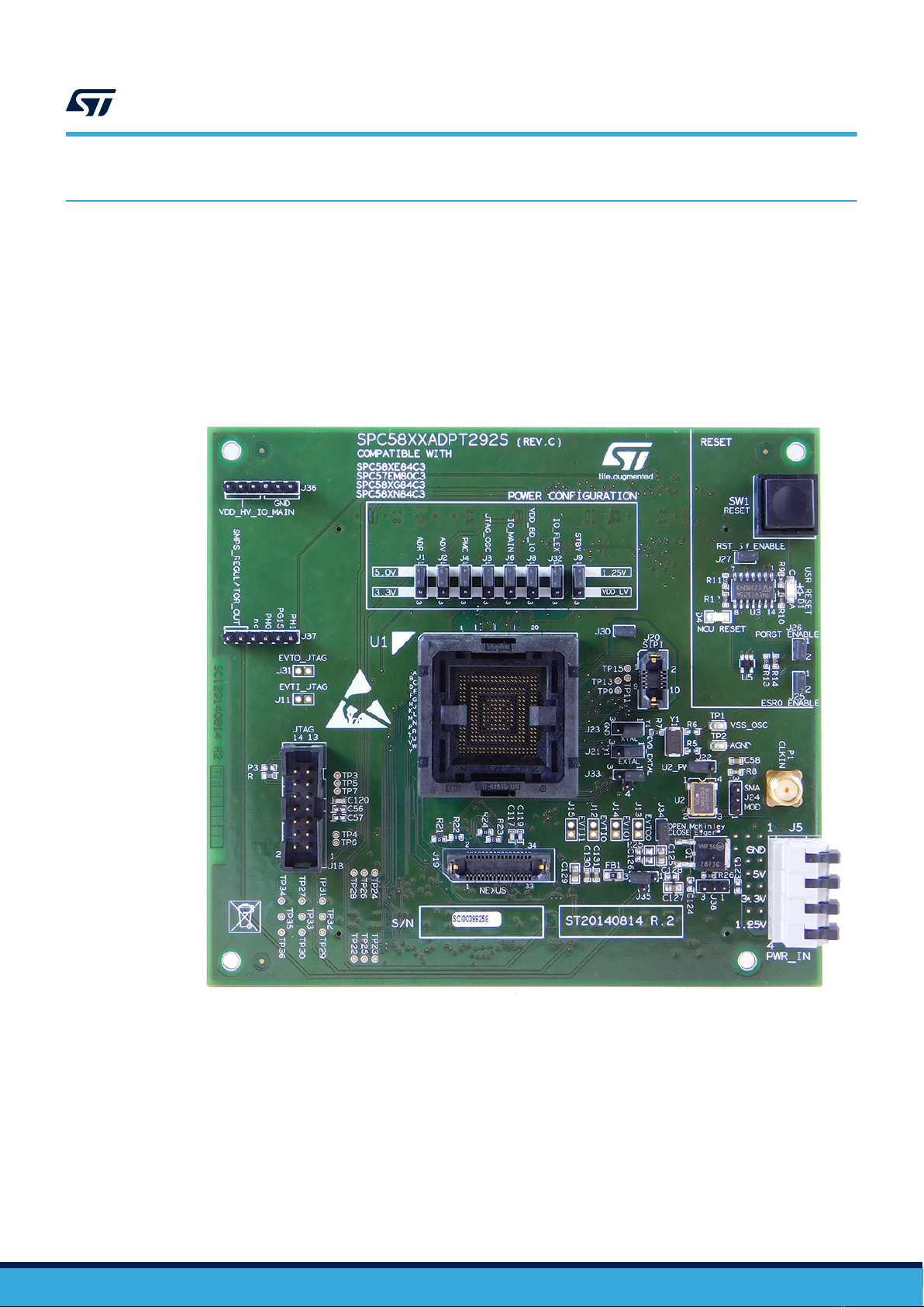
Table 1. Power configuration jumpers
Jumper Description Default Position
J1 VDD_HV_ADR voltage configuration
from 5.0V_LR or 3.3V_SR 1-2 (5.0V_LR) Figure 4. SPC58XXADPT292S Rev. C top "mini
module" view - B2
J2 VDD_HV_ADV voltage configuration
from 5.0V_LR or 3.3V_SR 1-2 (5.0V_LR) Figure 4. SPC58XXADPT292S Rev. C top "mini
module" view - B2
J3 VDD_HV_JTAG_OSC voltage
configuration from 5.0V_SR or 3.3V_SR 1-2 (5.0V_SR) Figure 4. SPC58XXADPT292S Rev. C top "mini
module" view - B2
J4 VDD_HV_PMC voltage configuration
from 5.0V_SR or 3.3V_SR 1-2 (5.0V_SR) Figure 4. SPC58XXADPT292S Rev. C top "mini
module" view - B2
J6 VDD_HV_IO_MAIN voltage
configuration from 5.0V_SR or 3.3V_SR 1-2 (5.0V_SR) Figure 4. SPC58XXADPT292S Rev. C top "mini
module" view - B2
J32 VDD_HV_IO_FLEX voltage
configuration from 5.0V_SR or 3.3V_SR 1-2 (5.0V_SR) Figure 4. SPC58XXADPT292S Rev. C top "mini
module" view - C2
J8 VDDPHYIO voltage configuration from
5.0V_SR or 3.3V_SR 1-2 (5.0V_SR) Figure 4. SPC58XXADPT292S Rev. C top "mini
module" view - C2
J9 VDD_LV_STBY voltage configuration
from 1.25V_SR or VDD_LV 1-2 (1.25V_SR) Figure 4. SPC58XXADPT292S Rev. C top "mini
module" view - C2
J35
VDD_LV voltage configuration from:
• BALLAST circuit
• 1.25V_SR
SMPS_REGULATOR_OUT
2-3 (1.25V_SR) Figure 4. SPC58XXADPT292S Rev. C top "mini
module" view - C4
J38
Supply for BALLAST circuit
configuration from VDD_HV_IO_MAIN
or 5.0V_SR
1-2
(VDD_HV_IO_MAIN)
Figure 4. SPC58XXADPT292S Rev. C top "mini
module" view - D2
UM2764
Power and system configuration
UM2764 - Rev 1 page 7/26

5.2 Microcolntroller configuration
The jumpers described in the following table needs to configure the board to use STMicroelectronics
microcontroller SPC57EM80C3.
Table 2. Microcontroller SPC57EM80C3 configuration related jumpers
Jumper Description Default Position
J33 Device ball T11 VDDSTBY
function configuration
2-3
(Connect VDDSTBY with
3.3_SR)
Figure 4. SPC58XXADPT292S Rev. C top "mini
module" view - C3
J34 Device ball N19 NC
function configuration
Open
(Device ball N19 Not Connected)
Figure 4. SPC58XXADPT292S Rev. C top "mini
module" view - C3
SW2
Device ball E15&D16
VDD_HV_FLA supply
configuration
2-3
(Disconnect VDD_HV_FLA from
VDD_HV_IO_MAIN)
Figure 5. SPC58XXADPT292S Rev. C bottom "mini
module" view - C2
The jumpers described in the following table need to configure the board to use STMicroelectronics
microcontrollers SPC58NE84C3, SPC58XG84C3 and SPC58XN84C3.
Table 3. SPC58NE84C3, SPC58XG84C3 and SPC58XN84C3 jumpers
Jumper Description Default Position
J33
Device ball T11 EXTREG_SEL
function configuration:
• 2-1 (DISABLE BALLAST)
• 2-4 (ENABLE BALLAST)
2-1 (DISABLE BALLAST) Figure 4. SPC58XXADPT292S Rev. C top "mini
module" view - C3
J34 Device ball N19 NC function
configuration
Close
(Connect BCTRL with
BALLAST Circuit)
Figure 4. SPC58XXADPT292S Rev. C top "mini
module" view - C3
SW2
Device ball E15&D16
VDD_HV_FLA supply
configuration
2-1
(Connect VDD_HV_FLA with
VDD_HV_IO_MAIN)
Figure 5. SPC58XXADPT292S Rev. C bottom
"mini module" view - C2
UM2764
Microcolntroller configuration
UM2764 - Rev 1 page 8/26

5.3 Port configuration
The following jumper need to configure the ports:
Table 4. Ports related jumpers
Jumper Description Default Position
J30 TESTMODE settings Close Figure 4. SPC58XXADPT292S Rev. C top "mini module" view - C2
J11 PF[15]/EVTI connection to QSH
motherboard connectors Open Figure 4. SPC58XXADPT292S Rev. C top "mini module" view - A2
J31 PH[11]/EVTO connection to QSH
motherboard connectors Open Figure 4. SPC58XXADPT292S Rev. C top "mini module" view - A2
J12 PM[4]/EVTI0 connection to QSH
motherboard connectors Open Figure 4. SPC58XXADPT292S Rev. C top "mini module" view - C3
J13 PM[5]/EVTO0 connection to QSH
motherboard connectors Open Figure 4. SPC58XXADPT292S Rev. C top "mini module" view - C3
J14 PM[6]/EVTO1 connection to QSH
motherboard connectors Open Figure 4. SPC58XXADPT292S Rev. C top "mini module" view - C3
J15 PK[14]/EVTI1 connection to QSH
motherboard connectors Open Figure 4. SPC58XXADPT292S Rev. C top "mini module" view - C3
UM2764
Port configuration
UM2764 - Rev 1 page 9/26

5.4 System clock configuration
The "mini module" supports the usage of crystal clock sources as well as external clock source:
Table 5. Clock configuration jumpers
Jumper Description Default Position
J21 40 MHz crystal clock source Enable
for pin EXTAL 1-2 (XT1 pin2) Figure 4. SPC58XXADPT292S Rev. C top "mini module"
view - C3
J23 40 MHz crystal clock source Enable
for pin XTAL 1-2 (XT1 pin1) Figure 4. SPC58XXADPT292S Rev. C top "mini module"
view - C3
J22 Enable 8 MHz oscillator power
supply Open Figure 4. SPC58XXADPT292S Rev. C top "mini module"
view - D3
J24 External clock source from 8 MHz
oscillator or SMA connector
1-2 (8 MHz
oscillator)
Figure 4. SPC58XXADPT292S Rev. C top "mini module"
view - D3
5.5 Reset circuit
The "mini module" supports different ways to reset the microcontroller.
To use and perform the reset driving there are different jumpers and switches:
Table 6. Reset configuration jumpers
Jumper Description Default Position
SW1 Reset push button Open Figure 4. SPC58XXADPT292S Rev. C top "mini module" view -
D1
J27
Connect the external reset to the reset
driver for
ESR0 and PORST pins
Close Figure 4. SPC58XXADPT292S Rev. C top "mini module" view -
D1
J25 Connect the external reset to ESR0
pin Close Figure 4. SPC58XXADPT292S Rev. C top "mini module" view -
D2
J26 Connect the external reset to PORST
pin Close Figure 4. SPC58XXADPT292S Rev. C top "mini module" view -
D2
UM2764
System clock configuration
UM2764 - Rev 1 page 10/26

5.6 Test points
The "mini module" has several test points. Below all test point description:
Table 7. Test points
Test Point Description Position
TP1 VSS_OSC test point Figure 4. SPC58XXADPT292S Rev. C top "mini module" view - D3
TP2 AGND test point Figure 4. SPC58XXADPT292S Rev. C top "mini module" view - D3
TP3 JCOMP test point Figure 4. SPC58XXADPT292S Rev. C top "mini module" view - A3
TP4 TCK test point Figure 4. SPC58XXADPT292S Rev. C top "mini module" view - A3
TP5 TMS test point Figure 4. SPC58XXADPT292S Rev. C top "mini module" view - A3
TP6 TDI test point Figure 4. SPC58XXADPT292S Rev. C top "mini module" view - A3
TP7 TDO test point Figure 4. SPC58XXADPT292S Rev. C top "mini module" view - A3
TP9 SIPI_RXN test point Figure 4. SPC58XXADPT292S Rev. C top "mini module" view - C2
TP11 SIPI_TXN test point Figure 4. SPC58XXADPT292S Rev. C top "mini module" view - C2
TP13 SIPI_RXP test point Figure 4. SPC58XXADPT292S Rev. C top "mini module" view - C2
TP15 SIPI_TXP test point Figure 4. SPC58XXADPT292S Rev. C top "mini module" view - C2
TP22 J16A, QSH connector, pin10 (PA5) test point Figure 4. SPC58XXADPT292S Rev. C top "mini module" view - A4
TP23 J16A, QSH connector, pin14 (PA9) test point Figure 4. SPC58XXADPT292S Rev. C top "mini module" view - B4
TP24 J16A, QSH connector, pin19 (PA14) test
point Figure 4. SPC58XXADPT292S Rev. C top "mini module" view - B4
TP25 J16A, QSH connector, pin12 (PA7) test point Figure 4. SPC58XXADPT292S Rev. C top "mini module" view - B4
TP26 J16A, QSH connector, pin13 (PA8) test point Figure 4. SPC58XXADPT292S Rev. C top "mini module" view - B4
TP27 J17B, QSH connector, pin209 (PD7) test
point Figure 4. SPC58XXADPT292S Rev. C top "mini module" view - A4
TP28 J16A, QSH connector, pin11 (PA6) test point Figure 4. SPC58XXADPT292S Rev. C top "mini module" view - A4
TP29 J17B, QSH connector, pin210 (PD6) test
point Figure 4. SPC58XXADPT292S Rev. C top "mini module" view - A4
TP30 J17B, QSH connector, pin183 (PF13) test
point Figure 4. SPC58XXADPT292S Rev. C top "mini module" view - A4
TP31 J17B, QSH connector, pin151 (PJ5) test
point Figure 4. SPC58XXADPT292S Rev. C top "mini module" view - A4
TP32 J17B, QSH connector, pin149 (PJ7) test
point Figure 4. SPC58XXADPT292S Rev. C top "mini module" view - A4
TP33 J17B, QSH connector, pin127 (PL9) test
point Figure 4. SPC58XXADPT292S Rev. C top "mini module" view - A4
TP34 J17B, QSH connector, pin125 (PL11) test
point Figure 4. SPC58XXADPT292S Rev. C top "mini module" view - A4
TP35 J17B, QSH connector, pin123 (PL13) test
point Figure 4. SPC58XXADPT292S Rev. C top "mini module" view - A4
TP36 J17B, QSH connector, pin121 (PL15) test
point Figure 4. SPC58XXADPT292S Rev. C top "mini module" view - A4
UM2764
Test points
UM2764 - Rev 1 page 11/26

5.7 Connectors
The "mini module" has other connectors described in the below table.
Table 8. Other connectors
Connectors Description Position
J20 10-pin header connector for SIPI
interface Figure 4. SPC58XXADPT292S Rev. C top "mini module" view - C2
J18 14-pin header connector for JTAG port Figure 4. SPC58XXADPT292S Rev. C top "mini module" view - A4
J19 34-pin SAMTEC connector for Nexus 2 Figure 4. SPC58XXADPT292S Rev. C top "mini module" view - B4
J36, J37 DC-DC Regulator Module Figure 4. SPC58XXADPT292S Rev. C top "mini module" view -
A1/A2
J16, J17
2 X SAMTEC QSH series, 240-way
connector to connect "mini module" to
Motherboard
Figure 5. SPC58XXADPT292S Rev. C bottom "mini module" view
J5 External power supplies input (5V, 3.3V,
1.25V) Figure 4. SPC58XXADPT292S Rev. C top "mini module" view - D4
P1 SMA Connector for External Clock Input Figure 4. SPC58XXADPT292S Rev. C top "mini module" view - D3
UM2764
Connectors
UM2764 - Rev 1 page 12/26

6Layout overview
Figure 4. SPC58XXADPT292S Rev. C top "mini module" view
1
2
3
4
ABCD
UM2764
Layout overview
UM2764 - Rev 1 page 13/26

Figure 5. SPC58XXADPT292S Rev. C bottom "mini module" view
1
2
3
4
ABCD
UM2764
Layout overview
UM2764 - Rev 1 page 14/26

7BOM
Table 9. BOM
Item Qty Reference Manufacturer code Value Part description
1 16
C1, C3, C5, C7, C10,
C12, C16, C18, C20,
C22, C24 ,C26, C28,
C30, C58, C59
100 nF Mult. cer. cap. 50V 0603
2 23
C2, C4, C6, C8, C11,
C13, C17, C19 ,C21,
C23, C25, C27, C29,
C31, C33, C36, C39,
C42, C45, C48, C51,
C54, C131
10 nF Mult. cer. cap. 50V 0603 (automotive series)
3 2 C14, C15 4.7 µF Mult.cer. cap. 16V 0805
4 9
C32, C35, C38, C41,
C44, C47, C50,C53,
C130
47 nF Mult. cer. cap. 50V 0603
5 13
C34, C37, C40, C43,
C46, C49, C52, C55,
C118, C121, C125,
C127, C129
2.2 µF Mult. cer. cap. 16V 0805 - automotive series
6 2 C56, C57 47 pF Mult. cer. cap. 50V 0603 - do not mount
7 2 C117, C119 100 pF Mult. cer. cap. 50V 0603
8 1 C120 27 pF Mult. cer. cap. 50 V 0603
9 1 C122 DNM Mult. cer. cap. 0805 - do not mount
10 4 C123, C124, C126,
C128 DNM Mult. cer. cap. 50V 0603 - do not mount
11 1 D1 Yellow Led diode yellow 1206
12 1 D4 Red Led diode red 1206
13 1 FB1 0R Resistor 1/10W 1% 0805
14 4
J1, J2, J3, J4, J6, J8,
J9, J21, J22, J23, J24,
J25, J26, J27, J30,
J32, J33, J34, J35,
J38
STRIP 2 mm Male strip, single row, vertical, golden, pitch
2 mm
15 1 J5 AST0250404 Conn 4 pin, 90°, AST board mount
screwless
16 6 J11, J12, J13, J14,
J15, J31 STRIP 2mm Male strip 20 poles, single row, vertical,
golden, pitch 2 mm - do not mount
17 2 J16, J17 Samtec
QSH-120-01-L-D-A Samtec 0.5 mm pitch high speed socket
18 1 J18 N2514-6002RB 3M conn flat male 14 pins, straight - pitch
2.54 mm
19 1 J19 Samtec ASP-137973-01 Samtec 0.8 mm pitch - connector SMD 17x2
- NEXUS connector
20 1 J20 ERF8-005-05.0-L-DV-L-TR Samtec 0.8 mm pitch rugged high speed
female connector
21 1 J36, J37 STRIP Male strip 36 pins pitch 2.54 180°
22 1 P1 CON 1 SMA Female RF SMA 180°
UM2764
BOM
UM2764 - Rev 1 page 15/26

Item Qty Reference Manufacturer code Value Part description
23 1 Q1 NJD2873 NPN plastic power transistor DPAK
24 9 R1, R2, R7, R20, R21,
R22, R23, R24, R26 0R Resistor 1/10W 1% 0603
25 1 R3 10K Resistor 1/10W 1% 0603 - do not mount
26 2 R4, R9 10K Resistor 1/10W 1% 0603
27 2 R5, R6 0R Resistor 1/10W 1% 0603 - Do not mount!
28 1 R8 100R Resistor 1/10W 1% 0603
29 2 R10, R12 560R Resistor 1/10W 1% 0603
30 3 R11, R13, R14 4K7 Resistor 1/10W 1% 0603
31 1 R25 DNM Resistor 1/10W 1% 0805 - Do not mount!
32 1 SW1 Pushbutton Pushbutton NO
33 1 SW2 CJS-1200TA1 CJS-1200TA1 CJS Microswitch slide SPDT SMD J-Lead
(1-2 closing)
34 2 TP1, TP2 Testpoint SMD PCB Test Point
35 24
TP3, TP4, TP5, TP6,
TP7, TP9, TP11,
TP13, TP15, TP22,
TP23, TP24, TP25,
TP26, TP27, TP28,
TP29, TP30, TP31,
TP32, TP33, TP34,
TP35, TP36
TEST POINT Testpoint SMD - ignore
36 1 U1 OTB-292(484RS)-0.8-002 SOCKET Socket for BGA292 -
OTB-292(484RS)-0.8-002 ENPLAS
37 1 U2 8 MHz Hybrid quartz osc ECS 3953M
38 1 U3 74LVC125AMTR I.C. Low Voltage CMOS quad bus buffers -
SO14
39 1 U5 74V1G08STR I.C. single 2-input and gate - SMD
SOT23-5L
40 1 Y1 NX5032GA 40 MHZ Quartz 40 MHz NX5032GA XTAL NDK
UM2764
BOM
UM2764 - Rev 1 page 16/26

8Schematics
Figure 6. Microcontroller power
separate ground for OSC & AGND
For layout: Check layout consideration
document for ground connection of
VSS_HV_ADR/V pins
VDD_LV
VDD_LV_STBY
VDD_HV_FLA
VDDPHYIO
VDD_HV_IO_FLEX
VDD_HV_IO_MAIN
VDD_HV_PMC
VDD_HV_JTAG_OSC
VDD_HV_ADV
VDD_HV_ADR
STBY_RAM_SUPPLY
Jumper conf. :
2-1: Eiger DISABLE BALLAST
2-4: Eiger ENABLE BALLAST
2-3: McKinely RAM SUPPLY
Jumper conf. :
Open /Close
McKinely/Eiger
FB Default resistor 0 ohm
thermal plane,
power 2W /3W
Jumper conf. :
2-1: Eiger
2-3: McKinely
STBY_RAM
GNDGND
VSS_OSC
5.0V_SR
3.3V_SR
VSS_OSC
GND
GND
AGND
GND
VDD_HV_IO_MAIN
GND
GND
GND
GND
3.3V_SR
1.25V_SR
5.0V_LR
5.0V_SR
AGND
GND
GND GND
1.25V_SR
GND GND
GNDGND
GND
GND
GND
GND
GND
AGND
AGND
GND GND
VSS_OSC
AGND
GND
GND
GND
GND GND
VDD_HV_IO_JTAG
3.3V_SR
GND
VDD_HV_IO_MAIN
GND
GND
GND
GND
GND
VDD_LV
VDD_LV
VDD_LV_PLL
VDD_LV_PLL
GND GND
VDD_HV_IO_MAIN
5.0V_SR
1.25V_SR
VDD_HV_IO_FLEX
SMPS_REGULATOR_OUT
C53
47nF
C37
2.2uF
X7R
J35
2
1
3
4
C3
100nF
TP1
1
C16
100nF
C46
2.2uF
X7R
C23
10nF
TP2
1
R26
0R
C7
100nF
J2
1
2
3
C20
100nF
C24
100nF
C5
100nF
C52
2.2uF
X7R
C130
47nF
X7R
C118
2.2uF
X7R
C128
DNP
J8
1
2
3
C122
DNP
R25
DNP
C124
DNP
J4
1
2
3
C2
10nF
C42
10nF
C44
47nF
C131
10nF
X7R
C48
10nF
J5
AST0250404
1
2
3
4
J6
1
2
3
C28
100nF
C4
10nF
C39
10nF
C14
4.7uF
X7R
C19
10nF
C8
10nF
J34
12
C27
10nF
C30
100nF
C129
2.2uF
X7R
C51
10nF
C6
10nF
J9
1
2
3
C41
47nF
J1
1
2
3
C34
2.2uF
X7R
C11
10nF
C54
10nF
C43
2.2uF
X7R
C121
2.2uF
X7R
J38
1
2
3
C35
47nF
Q1
NJD2873
D-PAK
B
E C
C49
2.2uF
X7R
C127
2.2uF
X7R
C18
100nF
C59
100nF
C45
10nF
C22
100nF
R2
0R
C21
10nF
C126
DNP
C10
100nF
C55
2.2uF
X7R
C15
4.7uF
X7R
C47
47nF
C31
10nF
C29
10nF
J32
1
2
3
FB1
0805
0R
R1
0R
C25
10nF
C32
47nF
C26
100nF
C50
47nF
C125
2.2uF
X7R
C123
DNP
C17
10nF
C33
10nF
J3
1
2
3
C12
100nF
SPC5XX 292BGA
POWER PINS
I/O (3.3V-5V)
PMC (5V)
ADC
OSC & JTAG (3.3 OR 5V)
FLEXRAY I/O (3.3V)
BUDDY I/O (3.3V-5V)
FLASH DECOUPLING
BUDDY CORE LOGIC (1.25V)
MCU CORE LOGIC (1.25V)
U1A
SOCKET
VDDSTBY/EXTREG_SEL T11
VSS_HV11
B2
VSS_HV8
D4
VSS_HV6
E5
VSS_HV10
A20
VSS_HV9
B19
VSS_HV7
D17
VSS_HV5
E16
VSS_HV4
T16
VSS_HV3
U17
VSS_HV2
W19
VSS_HV1
Y20
VDD_HV_IO_MAIN4 A2
VDD_HV_IO_MAIN3 B3
VDD_HV_IO_MAIN2 V19
VDD_HV_IO_MAIN1 W20
VDD_HV_IO_MAIN/PMC1 A19
VDD_HV_IO_MAIN/PMC2 B18
VDD_HV_FLEX D5
BD_VDD_LV_STDBY2 G8
BD_VDD_LV_STDBY1 H7
VDD_HV_ADR_S Y6
VDD_HV_ADR_D T1
VSS_HV_ADR_S
Y7
VSS_HV_ADR_D
T2
VSS_LV36
G9
VSS_LV31
H9
VSS_LV32
H10
VSS_LV29
J7
VSS_LV30
J8
VSS_LV27
J10
VSS_LV19
K8
VSS_LV20
K9
VSS_LV21
K10
VSS_LV13
L8
VSS_LV14
L9
VSS_LV15
L10
VSS_LV7
M7
VSS_LV8
M8
VSS_LV9
M10
VSS_LV3
N9
VSS_LV4
N10
VSS_LV2
P9
VSS_LV35
G12
VSS_LV33
H11
VSS_LV34
H12
VSS_LV28
J11
VSS_LV25
J13
VSS_LV26
J14
VSS_LV22
K11
VSS_LV23
K12
VSS_LV24
K13
VSS_LV16
L11
VSS_LV17
L12
VSS_LV18
L13
VSS_LV10
M11
VSS_LV11
M13
VSS_LV12
M14
VSS_LV5
N11
VSS_LV6
N12
VSS_LV1
P12
VDD_HV_IO_BD K14
VDD_HV_FLA1 D16
VDD_HV_FLA2 E15
VDD_LV4 N7
VDD_LV2 P8
VDD_LV6 G13
VDD_LV5 H14
VDD_LV3/VDD_LV_PLL N14
VDD_LV1 P13
NC/BCTRL N19
VSS_HV_OSC
L20
VDD_HV_ADV Y5
VSS_HV_ADV
Y4
NC/VDD_LV L14
VDD_HV_IO_JTAG/PM N20
C1
100nF
C36
10nF
C40
2.2uF
X7R
SW2
CJS-1200TA1
2
1
3
J33
2
1
3
4
C13
10nF
C38
47nF
UM2764 - Rev 1 page 17/26
UM2764
Schematics

Figure 7. Microcontroller I/O
Port pins and reset signal
are routed to motherboard.
High speed signals are not
routed to motherboard, but have
test points to connect to test
on motherboard connector
EVT signal are connected to optional
jumper to be routed to motherboard.
LVDS Test points & off page
connector s
differential signals
PB0
PB1
PB2
PB3
PB4
PB5
PB6
PB7
PB8
PB9
PB10
PB11
PB12
PB13
PB14
PB15
PD0
PD1
PD2
PD3
PD4
PD5
PD8
PD9
PD10
PD11
PD12
PD13
PD14
PD15
PF0
PF1
PF2
PF3
PF4
PF5
PF6
PF7
PF8
PF9
PF10
PF11
PF12
PF14
PH0
PH1
PH2
PH3
PH4
PH5
PH6
PH7
PH8
PH9
PH10
EVTO
PH12
PH13
PH14
PH15
PJ0
PJ1
PJ2
PJ3
PJ4
PJ6
PJ8
PJ9
PJ10
PJ11
PJ12
PJ13
PJ14
PJ15
PL0
PL1
PL2
PL3
PL4
PL5
PL6
PL7
PL10
PL12
PL14
TX2N
TX2P
TX3N
TX3P
ESR0
PORST
XTAL
EXTAL
PF15
SIPI_TXN
TX0P
EVTI1
PK14
EVTO1
EVTO0
PM4
PM5
PM6
EVTI0
SIPI_RXP
SIPI_RXN
SIPI_RXN
CLKP
CLKN
TX1N
TX1P
TX0N
SIPI_RXP
SIPI_TXN
SIPI_TXP
PK2
PC5
PE1
EVTI0
PI2
PI7
PA12
PC15
PA1
PI9
PE3
PA3
PI13
PE15
EVTO1
PM2
PE10
PA0
PK13
PG3
PI14
PC1
PI3
PI10
PE8
PG1
PE0
PC6
PE14
PE2
PM8
PK15
PK7
PI6
PA2
PC12
PM10
PE4
SIPI_TXP
PI15
PE7
PI11
PG11
PC8
PE11
PM9
PE12
PC2
PE5
PI12
PG12
PC14
PG2
PC0
PI1
PK6
PK10
PM7
PM1
PG10
PK8
PG6
PC9
PA13
PE6
PG9
PC7
PC10
PA11
PC13
PK1
PG14
PC4
PI5
PA15
PE13
EVTI1
PK5
PK4
PK11
PK3
PM3
PK9
PG5
PA10
PG15
EVTO0
PG8
PE9
PC11
PK12
PK0
PI8
PG0
PG13
PC3
PI4
PM0
PG4
PA4
PI0
PG7
EVTI
CLKN
CLKP
TX1P
TX1N
TX0P
TX0N
TX2N
TX2P
TX3N
TX3P
PH11EVTO
PL8
PM12
PM11
JCOMP
TMS
TDI
TCK
TDO
GND
GND
PA[0..15]
(pg5)
PK14
(pg5)
)
5
g
p( 4
M
P
)5gp( 5MP
)5gp( 6MP
SIPI_RXN (pg6)
SIPI_TXN (pg6)
SIPI_RXP (pg6)
SIPI_TXP (pg6)
EVTI(pg6 )
PF15 (pg5)
ESR0 (pg6 ,7)
PORST (pg6,7)
XTAL(pg7)
EXTAL(pg7 )
PM[0..12](pg5)
PK[0..15]
(pg5)
PI[0..15](pg5)
PG[0..15](pg5)
PE[0..15](pg5)
PC[0..15](pg5 )
PB[0..15] (pg5)
PD[0..15] (pg5)
PF[0..15] (pg5,6)
PH[0..15] (pg5)
PJ[0..15] (pg5)
PL[0..15] (pg5 )
EVTI0
(pg6)
EVTO0
(pg6)
EVTO1
(pg6)
EVTI1(pg6)
CLKP (pg6)
CLKN (pg6 )
TX1N(pg6 )
TX1P(pg6 )
TX0N(pg6 )
TX0P(pg6 )
TX2N(pg6 )
TX2P(pg6 )
TX3N(pg6 )
TX3P(pg6 )
PH11 (pg5 )
EVTO (pg6)
JCOMP
(pg6)
)6g
p
( K
C
T
)
6
g
p
(S
M
T
)6
g
p( I
DT
)
6
gp( O
D
T
TP11
TP4 TP5TP3 TP6 TP7
J14
DNP
1 2
J13
DNP
1 2
SPC5XX 292BGA
SIGNALS
U1B
SOCKET
PH[13] A3
PF[2] A4
PF[5] A5
PM[10]
A6
PH[15] A7
PC[11]
A8
PC[13]
A9
PE[12]
A10
PD[0] A11
PD[2] A12
PH[9] A13
PH[3] A14
PA[11]
A15
PM[9]
A16
PA[0]
A17
PA[1]
A18
PD[14] B1
PH[12] B4
PF[3] B5
PH[14] B6
PF[4] B7
PC[10]
B8
PC[12]
B9
PC[15]
B10
PD[1] B11
PD[3] B12
PH[4] B13
PE[10]
B14
PE[11]
B15
PA[10]
B16
PA[13]
B17
PA[2]
B20
PC[9]
C1
PD[15] C2
PA[12]
C19
PE[9]
C20
PC[7]
D1
PC[8]
D2
PM[2]
D6
PM[0]
D7
PK[14]
D8
PC[14]
D9
PM[6]
D10
PH[7] D11
PH[8] D12
PH[10] D13
PH[1] D14
PH[0] D15
PD[5] D19
PE[8]
D20
PB[7] Y2
PB[6] Y3
PG[12]
Y8
PE[13]
Y9
PI[12]
Y10
PI[10]
Y11
PF[0] Y12
PD[10] Y13
PB[10] Y14
PB[8] Y15
PD[8] Y16
PF[6] Y17
PJ[0] Y18
PJ[1] Y19
PG[5]
W1
PG[6]
W2
PI[6]
W3
PI[7]
W4
PG[8]
W5
PG[9]
W6
PG[11]
W7
PE[15]
W8
PB[2] W9
PI[13]
W10
PI[11]
W11
PF[1] W12
PD[9] W13
PB[11] W14
PB[9] W15
PA[3]
W16
PF[7] W17
PA[15]
W18
PI[4]
V1
PI[5]
V2
PJ[2] V20
PI[3]
U2
PG[7]
U5
PK[11]
U6 PK[10]
U7
PE[14]
U8
PB[3] U9
PB[1] U10
PL[9]/TX1N U11
PL[11]/TX1P U12
PL[13]/TX0N U13
PL[15]/TX0P U14
PJ[7]/CLKN U15
PJ[5]/CLKP U16
PF[8] U19
PJ[3] U20
PI[2]
U1
PK[7]
T4
PK[8]
T5
PK[9]
T6
PG[10]
T7
PB[4] T8
PD[11] T9
PB[0] T10
NC/ PL[8] A1
PL[10] T12
PL[12] T13
PL[14] T14
PJ[6] T15
PH[6] T17
PJ[4] T19
PH[5] T20
PI[0]
R1
PB[5] R2
PF[11] R20
PK[4]
R4
PK[6]
R5
PJ[8] R16
PJ[9] R17
PF[12] R19
PC[5]
E1
PC[6]
E2
PL[1] E4
PM[3]
E6
PM[1]
E7
PK[15]
E8
PM[4]
E9
PM[5]
E10
PM[7]
E11
PM[8]
E12
PH[2] E13
PG[15]
E14
PE[6]
E17
PE[7]
E19
PD[4] E20
PC[3]
F1
PC[4]
F2
PE[5]
F20
PL[2] F4
PL[0] F5
ESR0 F16
PG[13]
F17
PG[14]
F19
PC[2]
G1 PC[1]
G2
PL[3] G4
PL[4] G5
LPBK_N G10
LPBK_P G11
PA[4]/ESR1
G16
PORST G17
PH[11] G19
PF[15] G20
PB[15] P1
PB[13] P2
PI[1]
P4
PK[5]
P5
TX2N P10
TX2P P11
PJ[10] P16
PJ[11] P17
PF[10] P19
PF[9] P20
PC[0]
H1
PE[0]
H2
PF[14] H20
PL[6] H4
PL[5] H5
PA[9]/TDO
H16 PA[8]/TDI
H17
TESTMODE H19
PE[1]
J1
PE[2]
J2
PD[12] J4
PL[7] J5
PA[6]/TCK
J16
PI[15]
J17
PD[7] J19
PA[14]
J20
PD[13] K1
PE[4]
K2 PE[3]
K4
PG[0]
K5
TX3P K7
PA[7]/TMS
K16
PI[14]
K17
PF[13] K19
PD[6] K20
PG[4]
N1 PG[3]
N2
PB[12] N4
PB[14] N5
PJ[13] N16
PJ[12] N17
PG[2]
M1 PG[1]
M2
PK[2]
M4
PK[3]
M5
PJ[15] M16
PJ[14] M17
XTAL M19
EXTAL M20
PI[8]
L1
PI[9]
L2
PK[0]
L4
PK[1]
L5
TX3N L7
PK[13]
L16 PK[12]
L17
PA[5]
L19
NC/ PM[12]
Y1 NC/ PM[11]
U4
J12
DNP
1 2
J30
STRIP 2mm
12
J15
DNP
1 2
J31
STRIP 2mm
DNP
12
TP15
TP13
TP9
J11
STRIP 2mm
DNP
12
UM2764 - Rev 1 page 18/26
UM2764
Schematics

Figure 8. Board connector
PortE PortF PortG PortH PortIPortC PortJ PortK PortL
PortA PortB Port D
PortM
PK1
PK5
PK7
PK9
PK11
PK3
PK13
PK15
PK2
PK4
PK6
PK8
PK10
PK0
PK12
PK14
PI2
PI4
PI6
PI0
PI8
PI10
PI12
PI14
PG2
PG0
PG4
PG6
PG8
PG10
PG12
PG14
5.0V_SR
PE2
PE4
PE6
PE8
PE0
PE10
PE12
PE14
1.25V_SR
PC0
PC2
PC4
5.0V_SR
PC6
PC8
PC10
PC12
PC14
3.3V_SR
1.25V_SR
PA0
PA2
PA4
PA10
PA12
5.0V_SR
PI1
PI5
PI7
PI3
PI9
PI11
PI13
PI15
PG1
PG3
PG5
PG7
PG9
PG11
PG13
PG15
5.0V_SR
PE1
PE11
PE13
PE15
1.25V_SR
PE5
PE7
PE9
PE3
PC1
PC5
PC7
PC3
PC9
PC11
PC13
PC15
3.3V_SR
1.25V_SR
PA3
PA1
PA11
PA13
PA15
5.0V_SR
1.25V_SR
3.3V_SR
1.25V_SR
5.0V_SR 5.0V_SR
1.25V_SR
3.3V_SR
5.0V_SR
1.25V_SR 5.0V_LR
PM3
PM5
PM1
PM7
PM9
PM0
PM2
5.0V_LR
PM4
PM6
PM8
PM10
5.0V_LR 5.0V_LR
3.3V_SR
3.3V_SR
5.0V_SR
5.0V_SR
1.25V_SR
1.25V_SR
RST-SW
3.3V_SR
3.3V_SR
5.0V_SR
5.0V_SR
1.25V_SR
1.25V_SR
VDD_HV_IO_MAIN VDD_HV_IO_MAIN
VDD_HV_IO_MAIN
VDD_HV_IO_MAIN
PE12
PE13
PE14
PE15
PF0
PF1
PF2
PF3
PF4
PF5
PF6
PF7
PF[0..15]
PF8
PF9
PF10
PF11
PF12
PF14
PF15
PG0
PG1
PG2
PG3
PG4
PG5
PG6
PG7
PG[0..15]
PG8
PG9
PG10
PG11
PG12
PG13
PG14
PG15
PH0
PH1
PH2
PH3
PH4
PH5
PH6
PH7
PH[0..15]
PH8
PH9
PH10
PH11
PH12
PH13
PH14
PH15
PI0
PI1
PI2
PI3
PI4
PI5
PI6
PI7
PI[0..15]
PI8
PI9
PI10
PI11
PI12
PI13
PI14
PI15
PC0
PC1
PC2
PC3
PC4
PC5
PC6
PC7
PC[0..15]
PC8
PC9
PC10
PC11
PC12
PC13
PC14
PC15
PJ0
PJ1
PJ2
PJ3
PJ4
PJ6
PJ[0..15]
PJ8
PJ9
PJ10
PJ11
PJ12
PJ13
PJ14
PJ15
PK0
PK1
PK2
PK3
PK4
PK5
PK6
PK7
PK[0..15]
PK8
PK9
PK10
PK11
PK12
PK13
PK14
PK15
PL0
PL1
PL2
PL3
PL4
PL5
PL6
PL7
PL[0..15]
PL8
PL10
PL12
PL14
PA0
PA1
PA2
PA3
PA4
PA[0..15]
PA10
PA11
PA12
PA13
PA15
PB0
PB1
PB2
PB3
PB4
PB5
PB6
PB7
PB[0..15]
PB8
PB9
PB10
PB11
PB12
PB13
PB14
PB15
PD0
PD1
PD2
PD3
PD4
PD5
PD[0..15]
PD8
PD9
PD10
PD11
PD12
PD13
PD14
PD15
PE0
PE1
PE2
PE3
PE4
PE5
PE6
PE7
PE[0..15]
PE8
PE9
PE10
PE11
PM0
PM1
PM2
PM3
PM4
PM5
PM6
PM7
PM[0..12]
PM8
PM9
PM10
1.25V_SR
5.0V_LR
3.3V_SR
5.0V_SR
VDD_HV_IO_MAIN
PB15
1.25V_SR
5.0V_SR
3.3V_SR
1.25V_SR
3.3V_SR
1.25V_SR
PL3
PL1
PL5
PL7
PJ1
PJ9
PJ11
PJ3
PJ13
PJ15
1.25V_SR
PH3
PH5
PH7
PH1
PH9
PH11
PH13
PH15
3.3V_SR
PF1
PF11
PF15
PF3
PF5
PF7
PF9
5.0V_SR
PD1
PD3
PD5
PD9
PD11
PD13
PD15
3.3V_SR
PB1
PB3
PB5
PB7
PB9
PB11
PB13
5.0V_LR
1.25V_SR
1.25V_SR
5.0V_SR
5.0V_SR
3.3V_SR
3.3V_SR
VDD_HV_IO_MAIN
5.0V_LR
VDD_HV_IO_MAIN
5.0V_LR
1.25V_SR
1.25V_SR
5.0V_SR
5.0V_SR
3.3V_SR
3.3V_SR
VDD_HV_IO_MAIN
5.0V_LR
VDD_HV_IO_MAIN
PL0
PL2
PL4
PL6
PL8
PL10
PL12
PL14
PJ0
PJ2
3.3V_SR
PJ4
PJ6
PJ8
PJ10
PJ12
PJ14
PH0
PH2
PH4
PH6
PH8
1.25V_SR
PH10
PH12
PH14
PF0
PF10
PF12
PF14
3.3V_SR
PF2
PF4
PF6
PF8
5.0V_SR
PD0
PD2
PD4
PD8
PD10
PD12
PD14
1.25V_SR
PB0
PB2
PB4
PB6
PB8
PB10
PB12
PB14
1.25V_SR
5.0V_SR
3.3V_SR
1.25V_SR
3.3V_SR
PM12
PM12
PM11
PM11
VDD_HV_IO_FLEX
VDD_HV_IO_FLEX
VDD_HV_IO_FLEX
VDD_HV_IO_FLEX
GND GND
3.3V_SR1.25V_SR 5.0V_LR5.0V_SR VDD_HV_IO_MAIN
GND GND
VDD_HV_IO_FLEX
PF[0..15](pg4,6) PG[0..15]
(pg4) PH[0..15]
(pg4) PI[0..15]
(pg4)PC[0..15](pg4) PJ[0..15]
(pg4) PK[0..15]
(pg4) PL[0..15]
(pg4)
PA[0..15]
(pg4) PB[0..15]
(pg4) PD[0..15]
(pg4) PE[0..15]
(pg4)
PM[0..12](pg4)
RST-SW(pg7)
TP28
TP26
TP24
J16B
SAMTEC QSH-120-01-L-D-A
SH1
SH1
SH2
SH2
SH3
SH3
SH4
SH4
SH5
SH5
SH6
SH6
SH7
SH7
SH8
SH8
SH9 SH9
121
121
123
123
125
125
127
127
129
129
131
131
133
133
135
135
137
137
139
139
141
141
143
143
145
145
147
147
149
149
151
151
153
153
155
155
157
157
159
159
161
161
163
163
165
165
167
167
169
169
171
171
173
173
175
175
177
177
179
179
181
181
183
183
185
185
187
187
189
189
191
191
193
193
195
195
197
197
199
199
201
201
203
203
205
205
207
207
209
209
211
211
213
213
215
215
217
217
219
219
221
221
223
223
225
225
227
227
229
229
231
231
233
233
235
235
237
237
239
239
SH16 SH16
SH15 SH15
SH14 SH14
SH13 SH13
SH12 SH12
SH11 SH11
SH10 SH10
122 122
124 124
126 126
128 128
130 130
132 132
134 134
136 136
138 138
140 140
142 142
144 144
146 146
148 148
150 150
152 152
154 154
156 156
158 158
160 160
162 162
164 164
166 166
168 168
170 170
172 172
174 174
176 176
178 178
180 180
182 182
184 184
186 186
188 188
190 190
192 192
194 194
196 196
198 198
200 200
202 202
204 204
206 206
208 208
210 210
212 212
214 214
216 216
218 218
220 220
222 222
224 224
226 226
228 228
230 230
232 232
234 234
236 236
238 238
240 240
TP29 TP27
TP30
TP22
TP31
TP32
TP25
TP33
J17A
SAMTEC QSH-120-01-L-D-A
11
33
55
77
99
11 11
13 13
15 15
17 17
19 19
21 21
23 23
25 25
27 27
29 29
31 31
33 33
35 35
37 37
39 39
41 41
43 43
45 45
47 47
49 49
51 51
53 53
55 55
57 57
59 59
61 61
63 63
65 65
67 67
69 69
71 71
73 73
75 75
77 77
79 79
81 81
83 83
85 85
87 87
89 89
91 91
93 93
95 95
97 97
99 99
101 101
103 103
105 105
107 107
109 109
111 111
113 113
115 115
117 117
119 119
2
24
46
68
810
10 12
12 14
14 16
16 18
18 20
20 22
22 24
24 26
26 28
28 30
30 32
32 34
34 36
36 38
38 40
40 42
42 44
44 46
46 48
48 50
50 52
52 54
54 56
56 58
58 60
60 62
62 64
64 66
66 68
68 70
70 72
72 74
74 76
76 78
78 80
80 82
82 84
84 86
86 88
88 90
90 92
92 94
94 96
96 98
98 100
100 102
102 104
104 106
106 108
108 110
110 112
112 114
114 116
116 118
118 120
120
TP23
TP34
TP35
TP36
J16A
SAMTEC QSH-120-01-L-D-A
1
1
3
3
5
5
7
7
9
9
11
11
13
13
15
15
17
17
19
19
21
21
23
23
25
25
27
27
29
29
31
31
33
33
35
35
37
37
39
39
41
41
43
43
45
45
47
47
49
49
51
51
53
53
55
55
57
57
59
59
61
61
63
63
65
65
67
67
69
69
71
71
73
73
75
75
77
77
79
79
81
81
83
83
85
85
87
87
89
89
91
91
93
93
95
95
97
97
99
99
101
101
103
103
105
105
107
107
109
109
111
111
113
113
115
115
117
117
119
119
22
44
66
88
10 10
12 12
14 14
16 16
18 18
20 20
22 22
24 24
26 26
28 28
30 30
32 32
34 34
36 36
38 38
40 40
42 42
44 44
46 46
48 48
50 50
52 52
54 54
56 56
58 58
60 60
62 62
64 64
66 66
68 68
70 70
72 72
74 74
76 76
78 78
80 80
82 82
84 84
86 86
88 88
90 90
92 92
94 94
96 96
98 98
100 100
102 102
104 104
106 106
108 108
110 110
112 112
114 114
116 116
118 118
120 120
J17B
SAMTEC QSH-120-01-L-D-A
SH1 SH1
SH2 SH2
SH3 SH3
SH4 SH4
SH5 SH5
SH6 SH6
SH7 SH7
SH8 SH8
SH9
SH9
121 121
123 123
125 125
127 127
129 129
131 131
133 133
135 135
137 137
139 139
141 141
143 143
145 145
147 147
149 149
151 151
153 153
155 155
157 157
159 159
161 161
163 163
165 165
167 167
169 169
171 171
173 173
175 175
177 177
179 179
181 181
183 183
185 185
187 187
189 189
191 191
193 193
195 195
197 197
199 199
201 201
203 203
205 205
207 207
209 209
211 211
213 213
215 215
217 217
219 219
221 221
223 223
225 225
227 227
229 229
231 231
233 233
235 235
237 237
239 239
SH16
SH16
SH15
SH15
SH14
SH14
SH13
SH13
SH12
SH12
SH11
SH11
SH10
SH10
122
122 124
124 126
126 128
128 130
130 132
132 134
134 136
136 138
138 140
140 142
142 144
144 146
146 148
148 150
150 152
152 154
154 156
156 158
158 160
160 162
162 164
164 166
166 168
168 170
170 172
172 174
174 176
176 178
178 180
180 182
182 184
184 186
186 188
188 190
190 192
192 194
194 196
196 198
198 200
200 202
202 204
204 206
206 208
208 210
210 212
212 214
214 216
216 218
218 220
220 222
222 224
224 226
226 228
228 230
230 232
232 234
234 236
236 238
238 240
240
UM2764 - Rev 1 page 19/26
UM2764
Schematics

Figure 9. JTAG, Nexus and SIPI
Place CAPS as close to
connector pins as
possible but do NOT fit
caps at board assembly.
JTAG Connector
(VSS)
(VSS)
(VSS)
(VSS)
JTAG interface
SIPI interface
DRCLK
Nexus interface
RDY not implemented on SPC57xxmM
TDI, TDO, TCK, TMS & JCOMP are not connected to
daughter card.
PORST, ESR0, EVTI and EVTO are connected to daughtercard
LVDS signals are not routed to motherboard.
JTAG signals are not routed to motherboard.
EVT signals have the option of adding a jumper on
daughtercard to route signals to motherboard.
Previson Eiger DC-DC Regulator
ball E14
(s mps_pmo s0 )
ball D15
(smps_vlx)
ball D14
(smps_nmos1)
EVTI
TDO
ESR0
TCK
TMS
TDI
JCOMP
TMS
JCOMP
PF14
SIPI_TXP
SIPI_TXN
TX0P
TX0N
TX1P
TX1N
TX2P
TX2N
TX3P
TX3N
TCK
TMS
TDI
TDO
JCOMP
EVTI1
EVTI0
EVTO0
PORST
ESR0
EVTO1
PORST
PORST
SIPI_RXN
SIPI_RXP
EVTO
PH0
PG15
PH1
VDD_HV_IO_JTAG
GND
GND
GND
GND GND
3.3V_SR
GND
VDD_HV_IO_JTAG
VDD_HV_IO_MAIN
GND
GND
TDI
(pg4,6)
TDO(pg4,6)
TCK(pg4,6)
)4
g
p
(IT
V
E
JCOMP
(pg4,6)
TMS
(pg4,6)
SIPI_TXP(pg4)
SIPI_TXN(pg4)
SIPI_RXN
(pg4)
SIPI_RXP(pg4)
TX0P
(pg4)
TX0N
(pg4)
TX1P
(pg4)
TX1N(pg4)
TX2P(pg4)
TX2N(pg4)
TX3P
(pg4)
TX3N
(pg4)
PF14 (pg4,5)
TCK (pg4,6)
TMS (pg4,6)
TDI (pg4,6)
TDO (pg4,6)
JCOMP (pg4,6)
EVTI1 (pg4)
EVTI0 (pg4)
EVTO0 (pg4)
PORST(pg4,6,7)
ESR0 (pg4,6,7)
CLKP (pg4)
CLKN (pg4)
EVTO1 (pg4)
ESR0(pg4,6,7)
PORST(pg4,6,7)
EVTO(pg4)
SMPS_REGULATOR_OUT
PH[0..15]
(pg4)
PG[0..15](pg4)
J37
STRIP
2
1
3
4
5
6
J20
ERF8-005-05.0-L-DV-L-TR
1 2
3 4
65
78
9 10
11 12
J18
N2514-6002RB
12
34
6
5
7 8
910
11 12
13 14
J19
SAMTEC ASP-137973-01
1
3
5
7
9
11
13
15
2
4
6
8
10
12
14
16
18
20
22
24
26
28
30
19
23
29
25
17
27
21
31 32
33 34
SH1 SH2
C117
100pF
R3
10K
DNP
R22 0R
C119
100pF
C57
47pF
DNP
C56
47pF
DNP
R4
10K
R23 0R
R20 0R
R24 0R
C120
27pF
J36
STRIP
2
1
3
4
5
6
R21 0R
UM2764 - Rev 1 page 20/26
UM2764
Schematics
Table of contents
Other ST Motherboard manuals

ST
ST FDA803S User manual

ST
ST NUCLEO-H745ZI-Q User manual

ST
ST STMPE801 User manual

ST
ST X-NUCLEO-S2868A1 User manual

ST
ST STEVAL-IPE005V1 User manual

ST
ST EVAL-L9963E-MCU User manual

ST
ST STEVAL-USBPD45H User manual

ST
ST X-NUCLEO-IDW01M1 User manual

ST
ST STEVAL-IHP007V1 User manual

ST
ST STEVAL-USBPD45H Administrator Guide