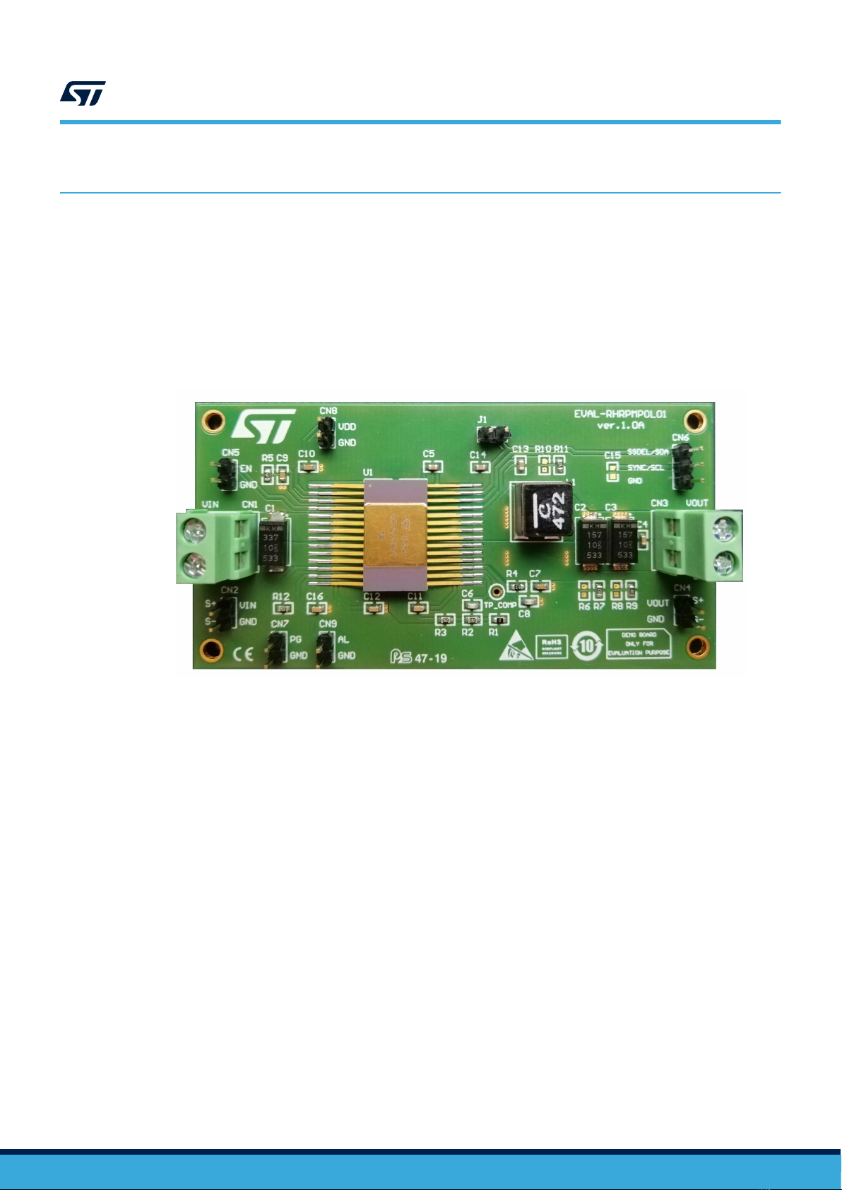
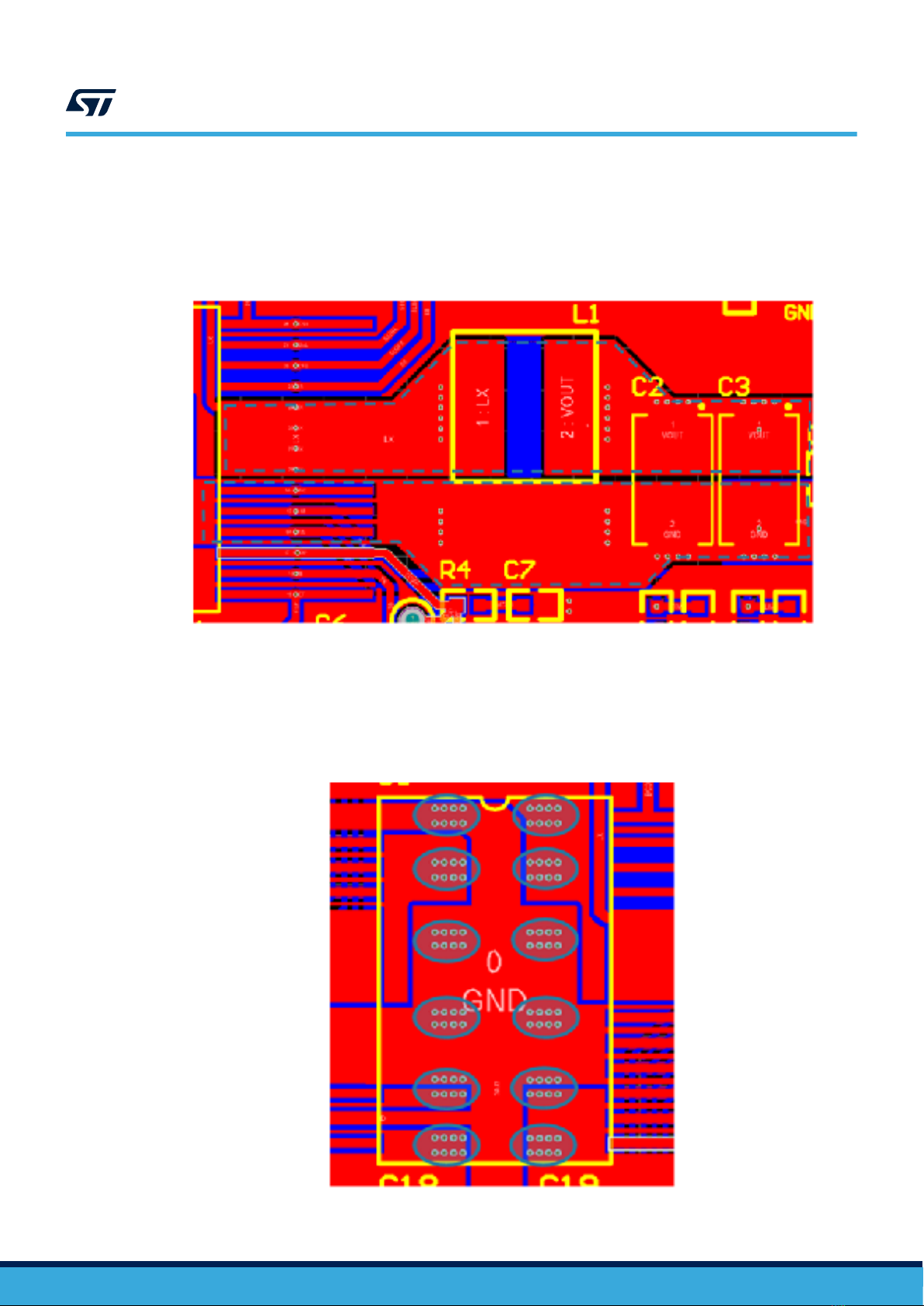
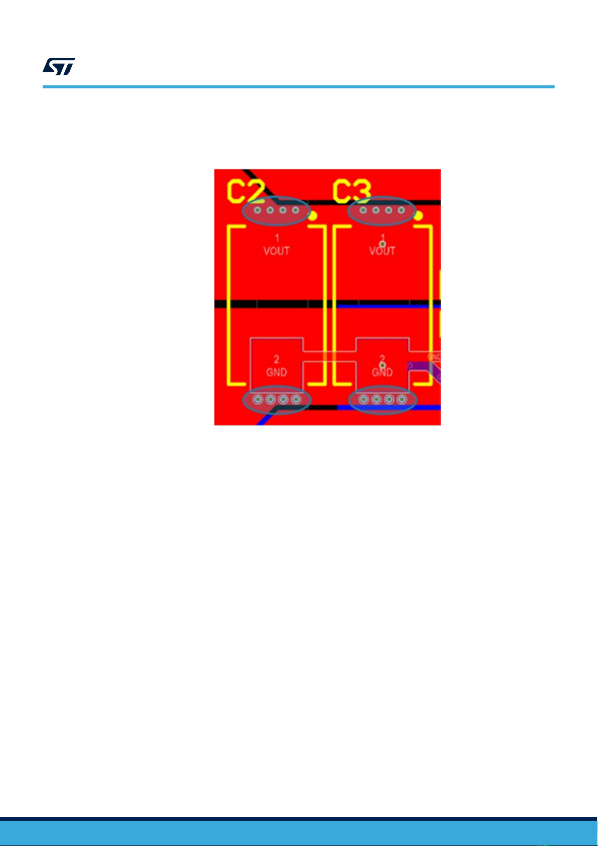
ST EVAL-RHRPMPOL01 User manual

Introduction
This user manual provides an overview of the use of the EVAL-RHRPMPOL01 evaluation board. It has been developed and
optimized for a typical application of the RHRPMPOL01 device, a single phase, step-down monolithic switching regulator with
high precision internal voltage reference and integrated power MOSFETs for synchronous conversion. The regulator
RHRPMPOL01 converts 3 V - 12 V input voltage to 0.8 V - (0.85xVIN) output voltage. The controller is based on a peak current
mode architecture, which ensures a fast load transient response and very stable switching frequency. An embedded integrator
compensates the DC voltage error due to the output voltage ripple.
General features:
• Input operating voltage: 5.0 V
• Output voltage: 1.2 V
• Output current: up to 5 A
• Enable input voltage: 2.5 V
• Switching frequency: 500 kHz
• Output overcurrent protection: 10 A
• Easy synchronization with 180 ° out-of-phase (up to 2 ICs) management
Figure 1. EVAL-RHRPMPOL01
• Orderable part number: EVAL-RHRPMPOL01
• Description: evaluation board of RHRPMPOL01
EVAL-RHRPMPOL01 evaluation board of radiation hardened 7 A monolithic
synchronous switching regulator
UM2706
User manual
UM2706 - Rev 1 - April 2020
For further information contact your local STMicroelectronics sales office.
www.st.com

1Schematic diagram
Figure 2. Schematic diagram
GND
GND
GND
2
1
CN1
1
2
CN4
1
2
CN3
GND
2
1
CN 2
330uF
C1
GND GND
GND
8.2K
R3
1uF
C11
VIN
5.0V
S+
S-
GND
VOUT
S+
S-
GND
4.7uHL1 VOUT
LX
EN
100nF
C13
100nF C14
GND
1uF
C9
GND
100nF
C5
GND
1uF
C10
GND
1uF
C12
GND
GND
27K
R4
GND
4.7K
R12 4.7nF
C7
SSDEL/SDA
SYNC/SCL
GND
SSDEL
3
2
1
CN6
GND
SYNC
VIN
VDD
VDD
EN
VCC
PGOOD
VDRIVE
REF
SS
FB
COMP
FSW
ILIM
SLOPE
I2C
SSDEL
SYNC
BOOST
GND
4.7
R5
VIN
GND
VIN
GND
VOUT
GND
100pF-NC
C15
VDRIVE 14
BOOT 28
VDD 2
VCC
3
EN
4
VIN4
8
PGND1
9
ILIM 19
SYNC
20
LX2 22
LX3 23
VIN2
6
VIN3
7
SS
25
VIN1
5
PGND2
10
LX1 21
LX4 24
SLOPE 26
SSDEL
27
PGND3
11
PGOOD
12
AL 13
AGND 1
FSW 18
COMP 17
FB 16
REF 15
U1
RHRPMPOL01
2
1
CN5
1uF
C16
GND
AL
3.9k
R2
270pF
C6
0
R1
GND
GNDGND
15pF
C8
GND
150uF
C3
150uF
C2
0.1uF
C4
0-NC
R6
50K
R7
0-NC
R8
1.2V
5 A
GND
1K
R9
0-NC
R10
12K
R11
VDDVDDVDD
2
1
CN7 PGOOD
GND
1
TP_COMP
COMP
PG
GND
2
1
CN8
VDD
GND
VDD
GND
2
1
CN9
AL
GND
AL.
GND
J1
Table 1. List of external components
Component Manufacturer Part number / description Value Size
C1 Kemet T530X337M010ATE006 330 µF 7343
C2,C3 Kemet T530D157M010ATE006 150 µF 7343
C4,C5,C13, C14 Murata GRM188R71H104KA93D 100 nF 0603
C9,C10, C11,C12, C16 Murata GRM188R61E105KA12D 1 µF 0603
C15 Murata GRM1885C1H101JA01 NC 0603
C6 Murata GRM1885C1H271JA01 270 pF 0603
C8 Murata GRM1885C1H150JA01 15 pF 0603
C7 Murata GRM188R71H472KA01 4.7 nF 0603
R4 Any Resistor 27 kΩ 0603
R1 Any Resistor 0 Ω 0603
R2 Any Resistor 3.9 kΩ 0603
R3 Any Resistor 8.2 kΩ 0603
R5 Any Resistor 4.7 Ω 0603
R12 Any Resistor 4.7 kΩ 0603
R6, R8,R10 Any Resistor NC 0603
R7 Any Resistor 50 kΩ 0603
R9 Any Resistor 1 kΩ 0603
R11 Any Resistor 12 kΩ 0603
UM2706
Schematic diagram
UM2706 - Rev 1 page 2/19

Component Manufacturer Part number / description Value Size
J1 Any 2-pin male strip line 2.54 mm pitch
CN1, CN3 Phoenix Contact 2-way PCB terminal 5.08 mm pitch
CN6 Any 3-pin male strip line 2.54 mm pitch
CN2, CN4,CN5, CN7, CN8, CN9 Any 2-pin male strip line 2.54 mm pitch
L1
Coilcraft XAL8080-472MEB
4.7 µH
8.60x8.10 mm
Wurth 7443330470 10.9x10.0 mm
TP Any Test point 0.9 hole size
U1 ST RH-PMPOL01KPX FLAT28
UM2706
Schematic diagram
UM2706 - Rev 1 page 3/19

2Input and output connections
Table 2. Input and output connections
Reference/Designator Name Description
CN1 VIN CN1_1: VIN power
CN1_2: GND power
CN2 VIN_SENSE CN2_1: VIN sense (s+)
CN2_2: GND sense (s-)
CN3 VOUT CN3_1: VOUT power
CN3_2: GND power
CN4 VOUT_SENSE CN4_1: VOUT sense (s+)
CN4_2: GND sense (s-)
CN5 EN CN5_1: EN pin
CN5_2: GND
CN6 SSDEL/SYNC
CN6_1: SSDEL/SDA pin
-J1: through a capacitor to GND
CN6_2: SYNC/SCL pin
CN6_3:GND
CN7 PGOOD CN7_1: PGOOD pin
CN7_2: GND
CN8 VDD CN8_1: VDD pin
CN8_2: GND
CN9 AL CN9_1: AL pin
CN9_2: GND
UM2706
Input and output connections
UM2706 - Rev 1 page 4/19

3Connectors
Figure 3. In/out connectors
1. Connect a power supply between VIN power (CN1_1) and GND power (CN1_2) and a power supply
between EN (CN5_1) and GND (CN5_2). The output voltage is present on VOUT pin at the voltage value
set by R1 and R2
2. Connect a multimeter between VIN (S+) (CN2_1) and GND (S-) (CN2_2) for a precise input voltage sensing
3. Connect a multimeter between VOUT (S+) (CN3_1) and GND (S-) (CN3_2) for a precise output voltage
sensing
4. Connect a multimeter between VDD (CN8_1) and GND (CN8_2) for a precise VDD voltage sensing. This pin
outputs a 2.7 V regulated voltage
5. R10 and R11 – SLOPE: the slope compensation ramp is programmed by connecting an external RSLOPE
resistor (R11) between the SLOPE pin and GND. The default internal slope compensation is also
implemented and it can be enabled by pulling up the voltage on SLOPE pin higher then 2 V or, better, up to
VDD by a resistor (R10) or simply by a short. If the SLOPE pin is directly shorted to GND, both ramps,
default current slope and programmed external current slope, are disabled
6. R8 and R9 – ILIM: the default value for the overcurrent threshold is 10 A, with a second level OCP of 13 A
(ILIM pin pulled up to VDD through R8). If a resistor (R9) is connected between ILIM pin and GND the ILIM1
threshold can be set to a lower value, and the ILIM2 will be consequently set at 1.3 x ILIM1
7. R6 and R7 – FSW: the regulator switching frequency can be programmed by connecting an external resistor
(R7) between FSW pin and GND. A voltage of 1 V is present on the FSW pin, so a current of 1 V/RFSW is
set on the resistor. This current is used to charge an internal capacitor (~20 pF). The switching frequency
can range from 100 kHz to 1 MHz. If the FSW pin is connected to a voltage higher than 2 V, (better if it is
shorted to VDD through R6), the external programmability is turned off and the internal default frequency,
tuned at 500 kHz, is enabled. To set “slave mode” configuration, FSW pin must be forced to a voltage lower
than 0.1 V or better shorted to ground. The internal clock is normally present to the SYNC pin with 180 °
phase shifting.
8. CN6 – SSDEL/SYNC: the device can also use the connectors on the demonstration board to directly control
the features through an I²C interface. In order to enable the serial interface the EN pin must be set to -2 V
and J1 has to be left open. Take care about capacitive load on pin SYNC: max. allowed capacitive load
(equivalent) for SLAVE devices is 150 pF
UM2706
Connectors
UM2706 - Rev 1 page 5/19

4Board layout guidelines
4.1 Guidelines
The DC-DC converter area is very sensitive, and it is necessary to pay attention to the layout of this part. This is
because the DC-DC converter generates GND noise that can get coupled with surrounding ground reducing the
sensitivity and high-frequency components can disturb the RF part of the system. To ensure a correct layout it is
necessary to provide efficient filtering by placing capacitors as close as possible to the device pins. To reduce
parasitic inductance and resistance, it is recommended to use connections as wide and short as possible.
Figure 4. Demo boards
4.2 Four-layer board
A four-layer board is strongly recommended, with top and bottom layers connected to ground (0 V). Use a ground
plane internally (mid layer) to reduce the coupling among the traces. Put this ground layer very close to the top
layer to obtain a good ground plane reference. A thickness between the top layer and ground layer of 0.2 mm or
0.3 mm is suggested.
If it is not possible to use a four-layer board, it is recommended to shield the area under the RF part (mainly
traces of LX and ground-current return paths) of the board with ground metal to reduce or eliminate radiation
emissions. Board routing and wiring should not be placed in this region to prevent coupling effects and to ensure
a good ground reference plane to the RF parts.
UM2706
Board layout guidelines
UM2706 - Rev 1 page 6/19

Figure 5. 4-layer board
4.3 Ground plane
Any switch mode power supply requires a good PCB layout in order to achieve the maximum performance.
Component placement, GND trace routing and width are the major issues. Basic rules commonly used for DC-DC
converters for good PCB layout should be followed. All traces carrying current should be drawn on the PCB as
short and thick as possible. This should minimize resistive and inductive parasitic effects, and increase system
efficiency. Suggested PCB (ring) ground plane avoids spikes on the output voltage. Good soldering of the
exposed pad helps on this issue.
Connect all the ground metallization and/or layers with as many vias as possible. Ground vias among layers
should be added liberally throughout the RF portion of the PCB. This helps prevent accrual of parasitic ground
inductance due to ground-current return paths. The vias also help to prevent cross- coupling from RF and other
signal lines across the PCB.
Figure 6. Ground plane
The layers assigned to system bias (DC supply) and ground must be considered in terms of the return current for
the components. The general guidance is not to have signals routed on layers between the bias layer and the
ground layer.
UM2706
Ground plane
UM2706 - Rev 1 page 7/19

Figure 7. Ground plane assignment
Figure 8. Ground plane assignment 2
4.4 Capacitor placing
Particular care has to be taken in the placement of the supply voltage filtering capacitors. It is, in fact, important to
ensure efficient filtering by placing these capacitors as close as possible to their dedicated pins on the
VIN,VREF,VFB,VDD and VDRIVE.
Figure 9. Capacitor placing
The layout of decoupling capacitors is extremely important to minimize the induction loop formed between the
capacitor and the IC power and ground. The vias should be placed on the side of the capacitor lands (at the
ends). The vias should be located at minimum keep-out distance and connected to the capacitor lands with a
wide trace, at least as wide as the via pad. Vias of opposite polarity should be placed as close together as
possible (minimum keep-out distance) and vias of the same polarity should be kept separated as much as
possible. If space allows, a second pair of vias on the opposite side of the capacitor may be added to further
reduce the inductance.
UM2706
Capacitor placing
UM2706 - Rev 1 page 8/19

4.5 Inductor placing
The DC-DC converter inductor has to be placed as close as possible to the LX pin, with short and thick traces.
This should minimize resistive parasitic effects, and increase system efficiency.
Figure 10. Inductor placing
4.6 Vias placing
It is crucial to connect very well the ground of the exposed pad of the FLAT28 to the ground on the application
board. This may be accomplished by placing many vias to be sure that the parasitic inductance introduced from
each via is negligible.
Figure 11. Vias placing
UM2706
Inductor placing
UM2706 - Rev 1 page 9/19

Connect all the ground metallization and/or layers with as many vias as possible. The vias should be located at
minimum keepout distance, in order to minimize resistive and inductive parasitic effects.
Figure 12. Vias placing 2
4.7 Feedback voltage
VFB is generated by a precision voltage divider (use of low tolerance resistors is recommended). Place a
decoupling capacitor very close to the VFB pin. Use good capacitor layout techniques. Place the voltage divider
resistors close to the VFB pin to minimize trace length, but not so close that they interfere with other critical signal
or power routing. Do not route the VFB trace near noisy traces or planes. Do not place a decoupling capacitor at
the junction of the resistors – only at the VFB pin.
UM2706
Feedback voltage
UM2706 - Rev 1 page 10/19

Figure 13. Feedback voltage
4.8 Thermal aspects
The RHRPMPOL01 power dissipation inside the IC is mainly due to the DC-DC integrated MOSFETs power loss.
The heat generated due to this power dissipation level requires a suitable heatsink to keep the junction
temperature below the overtemperature protection threshold at the rated ambient temperature. Try to increase,
where possible, the number of power planes connected, at least below the IC position, to improve the heat
dissipation. However, different layouts are also possible. Basic principles suggest:
• keeping the IC and its ground exposed pad approximately in the middle of the dissipating area
• to provide as many vias as possible
• to design a dissipating area having a shape as square as possible and not interrupted by other copper
traces
UM2706
Thermal aspects
UM2706 - Rev 1 page 11/19

Figure 14. Thermal aspects
UM2706
Thermal aspects
UM2706 - Rev 1 page 12/19

5Board layout
Figure 15. Assembly layer
Figure 16. Top layer
UM2706
Board layout
UM2706 - Rev 1 page 13/19

Figure 17. Mid layer1
Figure 18. Mid layer2
UM2706
Board layout
UM2706 - Rev 1 page 14/19

Figure 19. Bottom layer
UM2706
Board layout
UM2706 - Rev 1 page 15/19

Revision history
Table 3. Document revision history
Date Version Changes
14-Apr-2020 1 Initial release.
UM2706
UM2706 - Rev 1 page 16/19

Contents
1Schematic diagram ................................................................2
2Input and output connections......................................................4
3Connectors........................................................................5
4Board layout guidelines............................................................6
4.1 Guidelines ....................................................................6
4.2 Four-layer board ...............................................................6
4.3 Ground plane ..................................................................7
4.4 Capacitor placing...............................................................8
4.5 Inductor placing ................................................................9
4.6 Vias placing ...................................................................9
4.7 Feedback voltage .............................................................10
4.8 Thermal aspects ..............................................................11
5Board layout......................................................................13
Revision history .......................................................................16
UM2706
Contents
UM2706 - Rev 1 page 17/19

List of figures
Figure 1. EVAL-RHRPMPOL01 ...............................................................1
Figure 2. Schematic diagram ................................................................2
Figure 3. In/out connectors ..................................................................5
Figure 4. Demo boards .....................................................................6
Figure 5. 4-layer board .....................................................................7
Figure 6. Ground plane .....................................................................7
Figure 7. Ground plane assignment ............................................................8
Figure 8. Ground plane assignment 2 ...........................................................8
Figure 9. Capacitor placing ..................................................................8
Figure 10. Inductor placing ...................................................................9
Figure 11. Vias placing ......................................................................9
Figure 12. Vias placing 2.................................................................... 10
Figure 13. Feedback voltage ................................................................. 11
Figure 14. Thermal aspects .................................................................. 12
Figure 15. Assembly layer ................................................................... 13
Figure 16. Top layer ....................................................................... 13
Figure 17. Mid layer1 ...................................................................... 14
Figure 18. Mid layer2 ...................................................................... 14
Figure 19. Bottom layer..................................................................... 15
UM2706
List of figures
UM2706 - Rev 1 page 18/19

IMPORTANT NOTICE – PLEASE READ CAREFULLY
STMicroelectronics NV and its subsidiaries (“ST”) reserve the right to make changes, corrections, enhancements, modifications, and improvements to ST
products and/or to this document at any time without notice. Purchasers should obtain the latest relevant information on ST products before placing orders. ST
products are sold pursuant to ST’s terms and conditions of sale in place at the time of order acknowledgement.
Purchasers are solely responsible for the choice, selection, and use of ST products and ST assumes no liability for application assistance or the design of
Purchasers’ products.
No license, express or implied, to any intellectual property right is granted by ST herein.
Resale of ST products with provisions different from the information set forth herein shall void any warranty granted by ST for such product.
ST and the ST logo are trademarks of ST. For additional information about ST trademarks, please refer to www.st.com/trademarks. All other product or service
names are the property of their respective owners.
Information in this document supersedes and replaces information previously supplied in any prior versions of this document.
© 2020 STMicroelectronics – All rights reserved
UM2706
UM2706 - Rev 1 page 19/19
Table of contents
Other ST Motherboard manuals

ST
ST AN3954 Installation and operating instructions

ST
ST X-NUCLEO-IDB04A1 User manual

ST
ST SPC584B-DISP User manual

ST
ST STSW-STUSB002 User manual

ST
ST STEVAL-DIGAFEV1 User manual

ST
ST ST25DV-I2C User manual

ST
ST STEVAL-AETKT2V1 User manual

ST
ST STEVAL-PCC008V1 User manual

ST
ST SPC58XXADPT292S User manual

ST
ST STMPE801 User manual
Popular Motherboard manuals by other brands

MSI
MSI MS-CF06 user guide

Texas Instruments
Texas Instruments TLC6C5724-Q1 user guide

Analog Devices
Analog Devices DC353A quick start guide

Gigabyte
Gigabyte B660M AORUS ELITE AX DDR4 user manual

Linear Technology
Linear Technology DC980A manual

Freescale Semiconductor
Freescale Semiconductor M68HC12A4EVB user manual