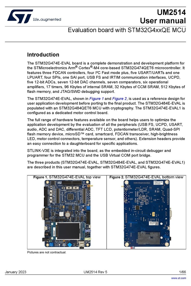
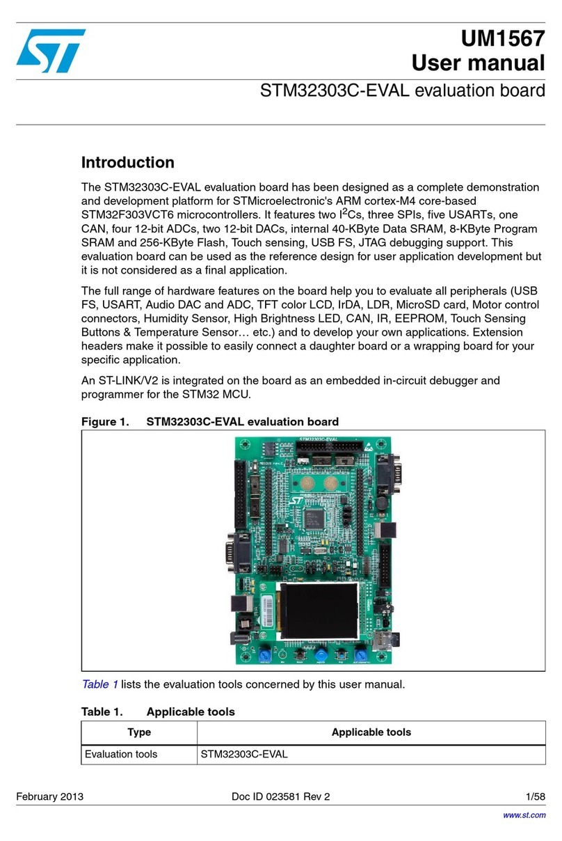
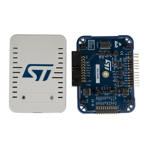
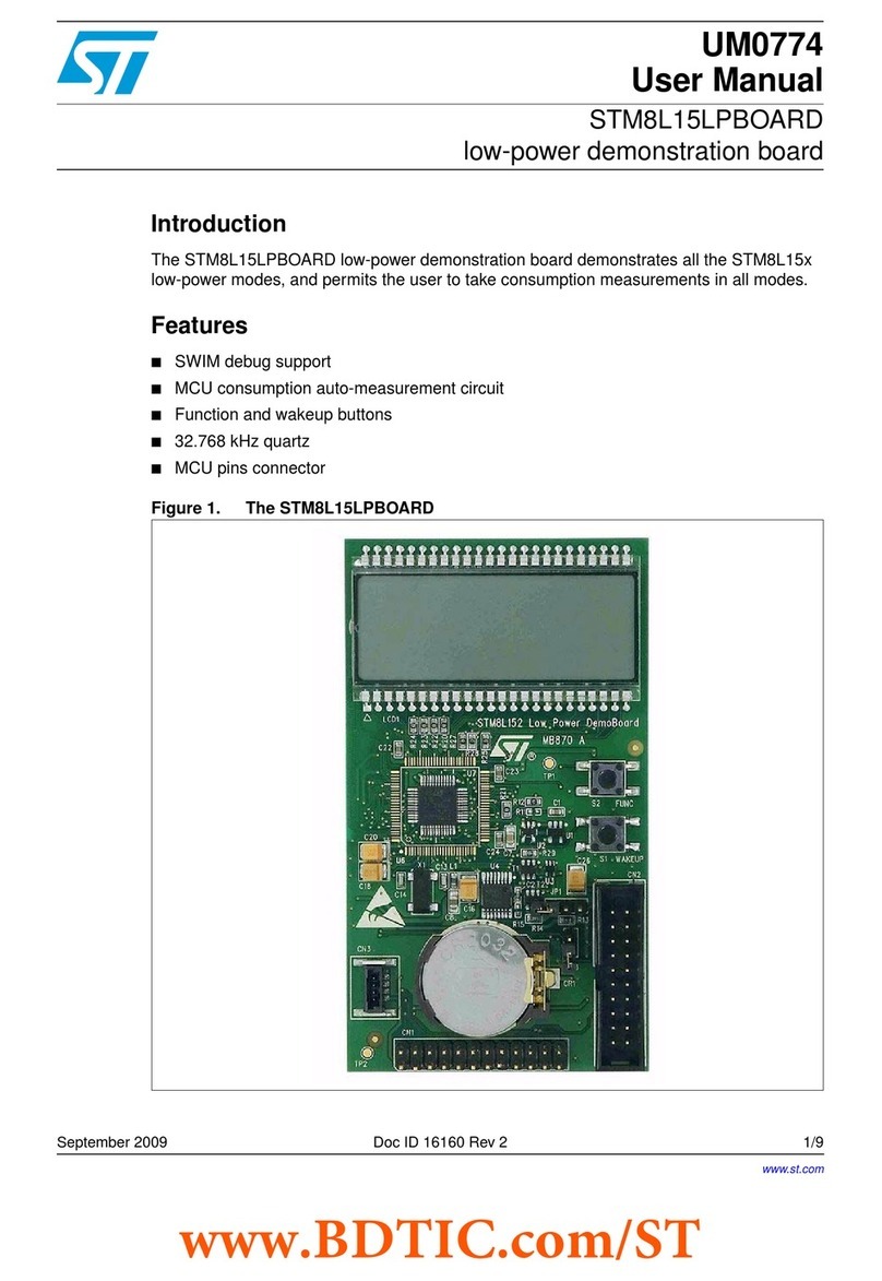
ST EVALSPEAr320CPU User manual

EVALSPEAr320CPU
SPEAr320 CPU
evaluation board
UM1015
User manual
Doc ID 18124 Rev 1
October 2010
www.st.com
STMicroelectronics

BLANK

October 2010 Doc ID 18124 Rev 1 3/38
UM1015
User manual
EVALSPEAr320CPU
SPEAr320 CPU evaluation board
Introduction
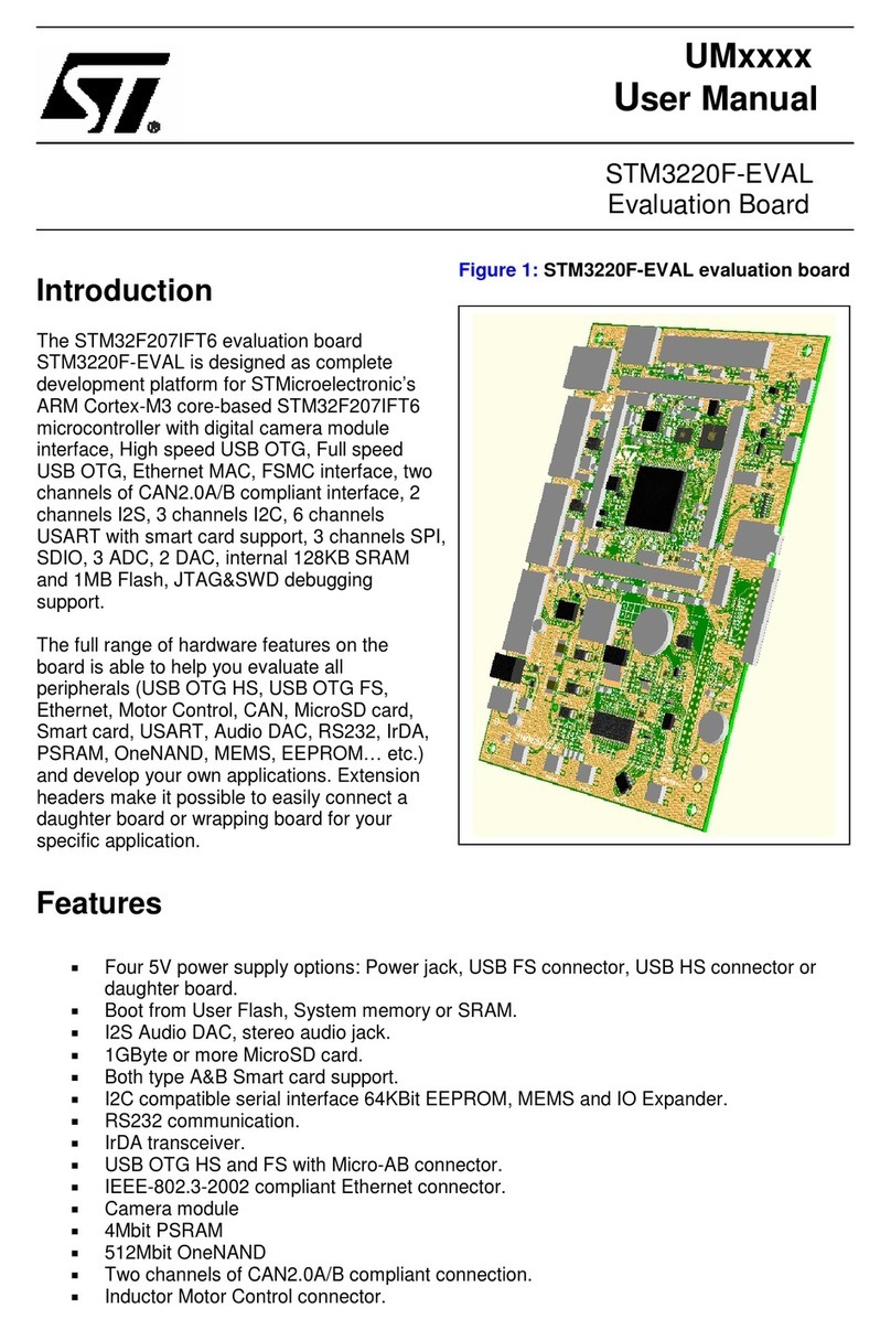
This document applies to revision 2.0 SPEAr320 CPU evaluation boards.
This board can be used to evaluate SPEAr320 microprocessors; the evaluation board kit
comprises one board, one serial cable interface, and one power supply.
CPU board features
■SPEAr320 embedded MPU
■Up to 2 Gbit DDR2 333 MHz (standard 128 Mbytes)
■Up to 16 Mbyte Serial Flash memory (standard 8 Mbytes)
■Two USB 2.0 full host port channels
■One USB 2.0 host device port
■One serial port (up to 115 baud)
■JTAG Debug ports
Figure 1. SPEAr320 CPU evaluation board
Top Bottom
www.st.com

Contents UM1015
4/38 Doc ID 18124 Rev 1
Contents
1 Getting started . . . . . . . . . . . . . . . . . . . . . . . . . . . . . . . . . . . . . . . . . . . . . . 7
1.1 Connections . . . . . . . . . . . . . . . . . . . . . . . . . . . . . . . . . . . . . . . . . . . . . . . . 7
1.2 Booting procedure . . . . . . . . . . . . . . . . . . . . . . . . . . . . . . . . . . . . . . . . . . . 7
2 Block diagram . . . . . . . . . . . . . . . . . . . . . . . . . . . . . . . . . . . . . . . . . . . . . . 8
3 Expansion connectors . . . . . . . . . . . . . . . . . . . . . . . . . . . . . . . . . . . . . . 11
4 Switch and jumper settings . . . . . . . . . . . . . . . . . . . . . . . . . . . . . . . . . . 15
4.1 Switch 1 settings . . . . . . . . . . . . . . . . . . . . . . . . . . . . . . . . . . . . . . . . . . . 15
4.2 Switch 2 settings . . . . . . . . . . . . . . . . . . . . . . . . . . . . . . . . . . . . . . . . . . . 16
4.3 Jumpers and connectors . . . . . . . . . . . . . . . . . . . . . . . . . . . . . . . . . . . . . 17
5 Board components . . . . . . . . . . . . . . . . . . . . . . . . . . . . . . . . . . . . . . . . . 18
6 Schematics . . . . . . . . . . . . . . . . . . . . . . . . . . . . . . . . . . . . . . . . . . . . . . . 22
7 Board layout . . . . . . . . . . . . . . . . . . . . . . . . . . . . . . . . . . . . . . . . . . . . . . . 31
8 Revision history . . . . . . . . . . . . . . . . . . . . . . . . . . . . . . . . . . . . . . . . . . . 32
8.1 Hardware revision history . . . . . . . . . . . . . . . . . . . . . . . . . . . . . . . . . . . . . 32
8.2 Document revision history . . . . . . . . . . . . . . . . . . . . . . . . . . . . . . . . . . . . 32
A License agreements. . . . . . . . . . . . . . . . . . . . . . . . . . . . . . . . . . . . . . . . . 33

UM1015 List of tables
Doc ID 18124 Rev 1 5/38
List of tables
Table 1. Switch SW1 bits [2:1] . . . . . . . . . . . . . . . . . . . . . . . . . . . . . . . . . . . . . . . . . . . . . . . . . . . . . . 9
Table 2. CPU board extension connector J12 . . . . . . . . . . . . . . . . . . . . . . . . . . . . . . . . . . . . . . . . . 11
Table 3. CPU board extension connector J13 . . . . . . . . . . . . . . . . . . . . . . . . . . . . . . . . . . . . . . . . . 13
Table 4. Switch 1 (SoC functional configuration) . . . . . . . . . . . . . . . . . . . . . . . . . . . . . . . . . . . . . . . 15
Table 5. Switch 1 (debug configuration) . . . . . . . . . . . . . . . . . . . . . . . . . . . . . . . . . . . . . . . . . . . . . . 15
Table 6. Switch 1 (functional configuration) . . . . . . . . . . . . . . . . . . . . . . . . . . . . . . . . . . . . . . . . . . . 15
Table 7. Switch 2 settings. . . . . . . . . . . . . . . . . . . . . . . . . . . . . . . . . . . . . . . . . . . . . . . . . . . . . . . . . 16
Table 8. CPU board components . . . . . . . . . . . . . . . . . . . . . . . . . . . . . . . . . . . . . . . . . . . . . . . . . . . 18
Table 9. Document revision history . . . . . . . . . . . . . . . . . . . . . . . . . . . . . . . . . . . . . . . . . . . . . . . . . 32

List of figures UM1015
6/38 Doc ID 18124 Rev 1
List of figures
Figure 1. SPEAr320 CPU evaluation board. . . . . . . . . . . . . . . . . . . . . . . . . . . . . . . . . . . . . . . . . . . . . 3
Figure 2. EVALSPEAr320CPU board block diagram. . . . . . . . . . . . . . . . . . . . . . . . . . . . . . . . . . . . . . 8
Figure 3. Serial cable setting . . . . . . . . . . . . . . . . . . . . . . . . . . . . . . . . . . . . . . . . . . . . . . . . . . . . . . . 9
Figure 4. 86-pin connectors (J12 and J13) . . . . . . . . . . . . . . . . . . . . . . . . . . . . . . . . . . . . . . . . . . . . 11
Figure 5. Schematic interconnections . . . . . . . . . . . . . . . . . . . . . . . . . . . . . . . . . . . . . . . . . . . . . . . . 22
Figure 6. DDR interface schematic . . . . . . . . . . . . . . . . . . . . . . . . . . . . . . . . . . . . . . . . . . . . . . . . . . 23
Figure 7. USB interface schematic . . . . . . . . . . . . . . . . . . . . . . . . . . . . . . . . . . . . . . . . . . . . . . . . . . 24
Figure 8. USB power and optional part schematic. . . . . . . . . . . . . . . . . . . . . . . . . . . . . . . . . . . . . . . 25
Figure 9. Miscellaneous interfaces schematic . . . . . . . . . . . . . . . . . . . . . . . . . . . . . . . . . . . . . . . . . . 26
Figure 10. Power supply schematic . . . . . . . . . . . . . . . . . . . . . . . . . . . . . . . . . . . . . . . . . . . . . . . . . . . 27
Figure 11. Customization interface schematic . . . . . . . . . . . . . . . . . . . . . . . . . . . . . . . . . . . . . . . . . . . 28
Figure 12. Daughterboard interface schematic . . . . . . . . . . . . . . . . . . . . . . . . . . . . . . . . . . . . . . . . . . 29
Figure 13. Schematic revision history . . . . . . . . . . . . . . . . . . . . . . . . . . . . . . . . . . . . . . . . . . . . . . . . . 30
Figure 14. SPEAr320 CPU evaluation board layout (top view) . . . . . . . . . . . . . . . . . . . . . . . . . . . . . . 31
Figure 15. SPEAr320 CPU evaluation board layout (bottom view) . . . . . . . . . . . . . . . . . . . . . . . . . . . 31

UM1015 Getting started
Doc ID 18124 Rev 1 7/38
1 Getting started
Warning: This board contains static sensitive devices.
The EVALSPEAr320CPU board is shipped in protective anti-static packaging. Do not submit
the board to high electrostatic potentials, and follow good practices for working with static
sensitive devices.
●Wear an anti-static wristband. Wearing a simple anti-static wristband can help
prevent ESD from damaging the board.
●Zero potential. Always touch a grounded conducting material before handling the
board, and periodically while handling it.
●Use an anti-static mat. When configuring the board, place it on and anti-static mat to
reduce the possibility of ESD damage.
●Handle only the edges. Handle the board by its edges only, and avoid touching board
components.
1.1 Connections
Refer to Figure 14 on page 31.
1. Connect a serial cable from connector J17 (serial link) to a host PC.
2. On the host PC running Windows or Linux, start the Terminal program.
3. Connect the +5 V voltage adapter (supplied in the EVALSPEAR320CPU package) to
the J11 power voltage connector on the CPU board.
4. Apply power to the board.
5. The Terminal program displays a sequence of boot messages followed by the Linux
console prompt.
For more information, refer to user manual UM0844 Getting started with Linux for SPEAr,
available at www.st.com/spear.
1.2 Booting procedure
The SPEAr320 CPU evaluation board can boot a Linux kernel that has been pre-installed in
the serial NOR Flash.
At power on, the serial port outputs a brief header message with some uBoot information
(uBoot version, SDK version, and some internal hardware information). At this point you can
choose to:
●Stop the system directly in uBoot: Press the spacebar on the host computer
keyboard before the boot delay time expires (default is 3 seconds).
●Boot Linux: The system logs you in automatically as super user, and displays the
Linux shell prompt on the screen.
Block diagram UM1015
8/38 Doc ID 18124 Rev 1
2 Block diagram
Figure 2. EVALSPEAr320CPU board block diagram
2.0.1 Dynamic memory subsystem
The Dynamic memory subsystem comprises three major parts:
Memory chip
The SPEAr320 MPU supports up to 256 Mbytes of memory. Place and route is provided for
2 chips but only one has been populated. The memory used is a Micron DDR2 device, its
part number is MT47H64M16HR-3 and its size is 128 Mbits x 8 (16 Mbits x 8 x 8 banks).
Local power supply
The local power supply is based on a monolithic voltage regulator for the chip set and
DDR2/3 (PM6641). It is generated locally in order to minimize the layout impact and also to
avoid any noise injection between different subsystems.
Signal termination
A parallel termination is added on the clock lines to compensate, if needed, for the layout
dissymmetry. Two 100k ohm resistors are used for each line in order to obtain an
impedance of 50 ohms. All the other terminations are directly inside the pads (both on the
SPEAr320 MPU and the memory sides).

UM1015 Block diagram
Doc ID 18124 Rev 1 9/38
2.0.2 Static memory subsystem (Serial Flash memory)
The SPEAr320 MPU supports up to 16 Mbytes of Serial Flash memory. Place and route for
2 blocks of 8 Mbytes are provided on the board, but only one is populated. It is based on an
M25P64-VMF6P (Numonix) Serial Flash memory device.
Resistor R8 protects the Flash memory from any unwanted write access.
2.0.3 USB 2.0 subsystem
Host ports
The board has two host ports that are fully compliant with the USB 2.0 specification (two
controllers with one port each). This means that the two hosts can work in concurrent mode
with the maximum possible bandwidth. Each host has also full control of the VBUS supplied
by the ST2052 power switch that also provides over current protection in case of a short
circuit in the USB cable.
Device port
The board has one USB 2.0 device port.
2.0.4 Debug interface
The JTAG interface can be used for static debugging, which means that it is possible to set
a breakpoint, and when the system stops, verify the contents of the memory or registers, or
both, and modify them if needed.
To select the debug feature, set Switch SW1 bits [2:1].
For more information on the ETM interface, refer to the trace box manufacturer’s
documentation (www.lauterbach.com, www.agilent.com, www.yokogawa.com).
2.0.5 Serial interface
One serial interface port is available. Typically used as an OS monitor, this port is available
on the J17 connector. It is possible to simulate a cross cable by changing the position of the
J22 jumpers.
Figure 3. Serial cable setting
Table 1. Switch SW1 bits [2:1]
Bit 2 Bit 1 Description
0 0 No debug features available
0 1 The ARM JTAG is connected to J4
Nul
Modem
Cable
J22
24
13
Cross
Cable
J22
24
13

Block diagram UM1015
10/38 Doc ID 18124 Rev 1
2.0.6 Real time clock (battery powered)
The real time clock (RTC) is powered by an external battery (3V) in order to prevent data
loss even if the main power supply is switched off.
2.0.7 General power supply
From a 5 V external AC/DC regulator power source, this block generates all the required
voltages as follows:
●1.2V (Switching regulator PM6641) to supply the internal logic of the SPEAr320 MPU
●1.8V (Switching regulator PM6641) for the DDR2 memory
●2.5V (LDO regulator) for the analog portion of SPEAr320
●3.3V (Switching regulator PM6641) to supply the other interfaces
A power monitor is also present to provide the general reset of the board.
2.0.8 Reset button
A manual reset button (P1) on the top of the board (see Figure 14 on page 31) resets the
microprocessor on the core board.

UM1015 Expansion connectors
Doc ID 18124 Rev 1 11/38
3 Expansion connectors
The CPU board has two 86-pin connectors (J12 and J13) that are used to extend the board.
On the board the connectors are horizontally center-aligned, and the distance between the
mechanical holes is 3400.00 th.
Tabl e 2 lists connector J12 pins.
Tabl e 3 on page 13 lists connector J13 pins.
Note: Connector through hole pins (10 pins) are connected to GND
Figure 4. 86-pin connectors (J12 and J13)
Table 2. CPU board extension connector J12
Pin Description Pin Description
1 +1.8V 2 +5V
3 +1.8V 4 +5V
5 +1.8V 6 +5V
7 +1.8V 8 +5V
9 PL_GPIO2 (RS232-TX LVTTL)(1) 10 PL_GPIO44
11 PL_GPIO3 (RS232-RX LVTTL)(2) 12 PL_GPIO39
13 RS232-TX(3) 14 PL_GPIO40
15 RS232-RX(4) 16 PL_GPIO38
17 PL_GPIO42 18 PL_GPIO29
19 PL_GPIO43 20 PL_GPIO37
21 PL_GPIO34 22 PL_GPIO30
23 PL_GPIO33 24 PL_GPIO28
25 PL_GPIO16 26 PL_GPIO26
27 PL_GPIO24 28 PL_GPIO27
29 PL_GPIO20 30 PL_GPIO9
31 PL_GPIO23 32 PL_GPIO13
33 PL_GPIO18 34 PL_GPIO8
1
2
75
76

Expansion connectors UM1015
12/38 Doc ID 18124 Rev 1
35 PL_GPIO11 36 PL_GPIO6
37 PL_GPIO19 38 PL_GPIO4
39 PL_GPIO15 40 PL_GPIO5
41 PL_GPIO14 42 NC
43 PL_GPIO36 44 NC
45 PL_GPIO41 46 NC
47 PL_GPIO35 48 NC
49 PL_GPIO31 50 +2.5V
51 PL_GPIO32 52 +2.5V
53 PL_GPIO25 54 +2.5V
55 PL_GPIO22 56 +2.5V
57 PL_GPIO21 58 INRESET
59 PL_GPIO17 60 nRESET
61 PL_GPIO12 62 +1.2V
63 PL_GPIO10 64 +1.2V
65 PL_GPIO7 66 +1.2V
67 PL_GPIO1 68 +1.2V
69 PL_GPIO0 70 +3.3V
71 NC 72 +3.3V
73 NC 74 +3.3V
75 NC 76 +3.3V
77
GND(5)
78
GND(5)
79 80
81 82
83 84
85 86
1. If J20 Jumper is set to pin2-3, otherwise NC.
2. If J21 Jumper is set to pin2-3, otherwise NC.
3. If J22 Jumper is set to pin2-4 and pin1-3, otherwise RS232-RX.
4. If J22 Jumper is set to pin2-4 and pin1-3, otherwise RS232-TX.
5. Physically connected to the internal metal plane of the connector. Pins 77 through 81 and 82 through 86
are shorted together.
Table 2. CPU board extension connector J12 (continued)
Pin Description Pin Description

UM1015 Expansion connectors
Doc ID 18124 Rev 1 13/38
Table 3. CPU board extension connector J13
Pin Description Pin Description
1 PL_GPIO47 2 +3.3V
3 PL_GPIO49 4 PL_GPIO63
5 PL_GPIO56 6 PL_GPIO46
7 PL_GPIO58 8 PL_GPIO57
9 PL_GPIO64 10 PL_GPIO61
11 PL_GPIO45 12 PL_GPIO66
13 PL_GPIO48 14 PL_GPIO69
15 PL_GPIO50 16 PL_GPIO72
17 PL_GPIO55 18 PL_GPIO73
19 PL_GPIO59 20 PL_GPIO70
21 PL_GPIO60 22 PL_GPIO67
23 PL_GPIO65 24 PL_GPIO71
25 PL_GPIO62 26 PL_GPIO75
27 PL_GPIO68 28 PL_GPIO82
29 PL_GPIO52 30 PL_GPIO76
31 PL_GPIO53 32 PL_GPIO85
33 PL_GPIO51 34 PL_GPIO87
35 PL_GPIO54 36 PL_GPIO95
37 PL_GPIO74 38 PL_GPIO79
39 PL_GPIO77 40 PL_GPIO94
41 PL_GPIO78 42 ADC VREFN
43 PL_GPIO81 44 AIN0
45 PL_GPIO80 46 GND
47 PL_GPIO84 48 AIN1
49 PL_GPIO83 50 GND
51 PL_GPIO86 52 AIN2
53 PL_GPIO91 54 GND
55 PL_GPIO90 56 AIN3
57 PL_GPIO96 58 GND
59 PL_GPIO88 60 AIN4
61 PL_GPIO89 62 GND
63 PL_GPIO92 64 AIN5
65 PL_GPIO93 66 GND
67 PL_GPIO97 68 AIN6
69 PL_CLK4 70 GND

Expansion connectors UM1015
14/38 Doc ID 18124 Rev 1
71 PL_CLK3 72 AIN7
73 PL_CLK2 74 GND
75 PL_CLK1 76 ADC VREFP
77
GND(1)
78
GND(1)
79 80
81 82
83 84
85 86
1. Physically connected to the internal metal plane of the connector. Pins 77 through 81 and 82 through 86
are shorted together.
Table 3. CPU board extension connector J13 (continued)
Pin Description Pin Description

UM1015 Switch and jumper settings
Doc ID 18124 Rev 1 15/38
4 Switch and jumper settings
4.1 Switch 1 settings
Note: When Switch SW1-x is in the ON position, the bit value is 0. When Switch 1 is in the OFF
position, the bit value is 1.
Bits 3, 4, 5 and 6 enable you to set the Functional configuration. The default configuration is
Configuration 3. For other configurations, refer to the SPEAr320 user manual available at
www.st.com/spear.
Table 4. Switch 1 (SoC functional configuration)
Bit Description
1 Test – see Debug configuration below
2 Reserved
3 Reserved
4 Reserved
5 Reserved
6 BootSel – see Debug configuration below
Table 5. Switch 1 (debug configuration)
Test bit Debug configuration
21
0 0 Normal Mode (No debug enabled)
0 1 ARM1 JTAG connected to J4
10Reserved
Table 6. Switch 1 (functional configuration)
Test bit
Functional configuration
6543
1011Configuration3

Switch and jumper settings UM1015
16/38 Doc ID 18124 Rev 1
4.2 Switch 2 settings
Note: If SW2-1 and SW2-2 are both off, B0 (pin PL_GPIO51) is in HiZ state, and can be controlled
from the application board.
If SW2-3 and SW2-4 are both off, B1 (pin PL_GPIO52) is in HiZ state, and can be controlled
from the application board.
If SW2-5 and SW2-6 are both off, B2 (pin PL_GPIO53) is in HiZ state, and can be controlled
from the application board.
If SW2-7 and SW2-8 are both off, B3 (pin PL_GPIO54) is in HiZ state, and can be controlled
from the application board.
SW2-1 and SW2-2 on: invalid condition
SW2-3 and SW2-4 on: invalid condition
SW2-5 and SW2-6 on: invalid condition
SW2-7 and SW2-8 on: invalid condition
Table 7. Switch 2 settings
Boot from SW2-1 SW2-2 SW2-3 SW2-4 SW2-5 SW2-6 SW2-7 SW2-8
USB_BOOT Off On Off On Off On Off On
ETH (parameter from I2C
ROM) On Off Off On Off On Off On
ETH (parameter from SPI
ROM) Off On On Off Off On Off On
Serial NOR (default setting) On Off On Off Off On Off On
Parallel NOR 8 (EMI with ACK) Off On Off On On Off Off On
Parallel NOR 16 (EMI with
ACK) On Off Off On On Off Off On
Parallel NAND 8 Off On On Off On Off Off On
Parallel NAND 16 On Off On Off On Off Off On
Reserved for SPI Off On Off On Off On On Off
Reserved for I²C On Off Off On Off On On Off
UART_BOOT Off On On Off Off On On Off
BootROM bypass On Off On Off Off On On Off
Parallel NOR 8 (EMI without
ACK) Off On Off On On Off On Off
Parallel NOR 16 (EMI without
ACK) On Off Off On On Off On Off
Reserved Off On On Off On Off On Off
Reserved On Off On Off On Off On Off

UM1015 Switch and jumper settings
Doc ID 18124 Rev 1 17/38
4.3 Jumpers and connectors
The jumpers and connectors numbered below refer to the CPU board schematics (available
on www.st.com/spear).
Sheet 4
●Connector J3 is a standard 20-pin 2.54 mm connector used for JTAG connections.
●Jumper J5 enables the power supply to the Real Time Clock block.
If jumper J5 is closed, the RTC is powered (standard).
●Connector J10 is a 2 vie 1.25 mm pitch connector for battery back-up with cable.
Sheet 5
●Connector J11 is a standard power connector for the ADC power supply with a 2.1-mm
central pitch.
Sheet 6
●Jumpers J6, J7, J8 and J9 are serial jumpers for the SPEAr power rail.
All jumpers MUST be closed. This configuration is used for power measurements.
Sheet 7
●Jumper J22 is a 4-pin symmetric IDC (or strip) connector that switches RX and TX
signals for different types of RS-232 cables(a):
– Two pins are connected to the ST3232 Receive/Transmit side.
– Two pins are connected to the RS-232 Receive/Transmit connector side.
●Connector J17 is a connector for standard IDC-to-DSUB converters.
●Jumper J20 switches between RS-232 transmit signals or GPIO2:
– If jumper is on pins 1 and 2, pin PL_GPIO2 is connected to U12 (ST3232) and the
COM0 is available on J17.
– If jumper is on pins 2 and 3, pin PL_GPIO2 is connected to the expansion
connector J12 pin 9. In this case the COM0 is available on CN13.
●Jumper J21 switches between RS-232 receive signals or GPIO3:
– If jumper is on pins 1 and 2, pin PL_GPIO3 is connected to U12 (ST3232) and the
COM0 is available on J17.
– If jumper is on pins 2 and 3, pin PL_GPIO3 is connected to the expansion
connector J12 pin 11. In this case the COM0 is available on CN13.
a. With 2 jumpers (inserted) it is possible to switch between two jumper inserted vertically and two jumpers
inserted horizontally. This enables the serial cable (null modem cable) to be adapted to the CPU board.

Board components UM1015
18/38 Doc ID 18124 Rev 1
5 Board components
Table 8. CPU board components
Component Designator Footprint Description
Capacitor
C1 C2 C3
C4 C5 C6
C7 C8 C9
C10 C11
C12 C13
C14 C15
C16 C17
C18 C19
C20 C21
C22 C23
C24 C25
C26 C27
C28 C29
C30 C31
C32 C33
C34 C35
C36 C37
C38 C39
C40 C41
C42 C43
C44 C45
C46 C47
C48 C49
C50 C56
C57 C58
C59 C60
C99 C100
C101 C102
0402 Ceramic capacitor 0.1uF 10% 10V X5R 0402
Resistor
R42 R43
R44 R45
R46 R47
R48 R50
0603 Resistor 0603 0 ohm
Resistor
R30 R31
R32 R33
R34 R35
R36 R37
R38 R72
R73 R74
0603 Resistor 0603 1k ohm 1% 0.1W
Inductor L3 LPS3.9X3.9 Power Inductor 1uH 1.7A 3.9x3.9mm SMD
Capacitor C89 0603 Ceramic capacitor 2.2nF 10% 50V X7R 0603
Inductor L1 L2 LPS3.9X3.9 Power Inductor 2.2uH 1.2A 3.9x3.9mm SMD
Resistor R59 R60 0603 Resistor 0603 4.3 ohm 1% 0.1W
Resistor R27 R28 0603 Resistor 0603 4.7k ohm 1% 0.1W

UM1015 Board components
Doc ID 18124 Rev 1 19/38
Resistor
R10 R11
R12 R13
R14 R15
R16 R17
R18 R19
R20 R21
R22 R23
R24 R25
R26
0603 Resistor 0603 10k ohm 1% 0.1W
Capacitor C75 C76
C77 0603 Ceramic capacitor 10 nF 10% 50V X7R 0603
Capacitor
C61 C62
C63 C64
C65 C66
C67 C68
C69 C70
C71 C72
C73 C74
C98
0805 Ceramic capacitor 10uF 10% 10V X5R 0805
Resistor R68 0603 Resistor 0603 15k ohm 1% 0.1W
Capacitor C78 C79 0603 Ceramic capacitor 15pF 5% 50V COG 0603
Capacitor C87 C88
C91 0603 Ceramic capacitor 22nF 10% 50V X7R 0603
Capacitor C93 1206 Ceramic capacitor 22 uF Y5V -20+80% 6.3V 1206
Crystal oscillator Y2 RAD-HC49 Crystal Oscillator 24MHz 30ppm through-hole
Resistor R70 0603 Resistor 0603 27k ohm 1% 0.1W
Crystal oscillator Y1 XT38T Crystal Oscillator 32.768KHz 20ppm d2x6mm
Capacitor C92 0603 Ceramic capacitor 33 nF 10% 50V X7R 0603
Capacitor C80 C81 0603 Ceramic capacitor 33pF 5% 50V COG 0603
Resistor R29 0805 Resistor 0805 43.2 ohm 0.1% 0.1W
Resistor R69 0603 Resistor 0603 47k ohm 1% 0.1W
Capacitor
C82 C83
C84 C85
C86 C94
C95 C96
C97
3528+ Tantalium Capacitor 47uF 10% 10V 3528-21
Resistor R49 0603 Resistor 0603 56k ohm 1% 0.1W
Resistor
R62 R63
R64 R65
R66 R67
0603 Resistor 0603 68k ohm 1% 0.1W
Resistor R61 0603 Resistor 0603 75k ohm 1% 0.1W
Resistor R2 R3 R4
R5 R6 R7 0603 Resistor 0603 100 ohm 1% 0.1W
Table 8. CPU board components (continued)
Component Designator Footprint Description

Board components UM1015
20/38 Doc ID 18124 Rev 1
Resistor R1 R53 0805 Resistor 0805 121k ohm 0.1% 0.1W
Resistor R55 R56
R57 0603 Resistor 0603 150 Kohm 1% 0.1W
Resistor R39 R40 0603 Resistor 0603 150 ohm 1% 0.1W
Resistor R75 0603 Resistor 0603 330 ohm 1% 0.1W
Resistor R58 0603 Resistor 0603 390k ohm 1% 0.1W
Resistor R8 R9 0603 Resistor 0603 470 ohm 1% 0.1W
Capacitor C90 0603 Ceramic capacitor 470 pF 10% 50V X7R 0603
Resistor R41 0603 Resistor 0603 680 ohm 1% 0.1W
Battery U8 BR2032 BATT BR2032: Coin type Lithium batterie 3V straight d20mm
Ferrite bead
FB3 FB4
FB5 FB6
FB7
0805 Ferrite Murata BLM21BD601SN1D
600 ohm/100MHz 200mA 0.35hm 0805
Diode D3 SOT23 Hi speed switching dual diode 200mA 70V
D BAV70
DC power socket J11 DPS2.5MM DC Power socket 2.5mm
DIP switch SW1 SWM-6X-SMD Surface mount 6-way micro dip switch pitch1.27mm
DIP switch SW2 SWM-8X-SMD Surface mount 8-way micro dip switch pitch1.27mm
Ferrite bead
FB8 FB9
FB12 FB13
FB14 FB15
FB10 FB16
0603 Ferrite 2506033007Y0 SMD 400mA
LED D5 D6 D7
D8 D9 0805P LED SMD 2,0 x 1,25mm Superbright Green
Connector J17 IDC5X2MD IDC 5X2 MD POL; IDC header 10pin p2.54mm straight male
polarized
Connector J3 IDC10X2MD IDC header 20pin p2.54mm straight male polarized
LED D1 D2 0805P Led SMD 2,0 x 1,25mm Superbright red
Memory U5 SO16 M25P64; Numonix 64Mbit SPI Serial Flash Memory 3.3V
16pin SO
Diode Z1 SOD123-C425 MMSZ5232BT1; Zener Diode 5.6V 0.5W
Connector J10 MLX-1.25MM-M MOLEX 1.25MM 2W M; Molex 1.25mm 2way male straight
SDRAM U2 U3 FBGA84 MT47H64M16HR3; MICRON DDR2 128MB 1.8V FBGA84
Transistor Q1 SOT23 NPN BC848; NPN transistor 30Vbc 5Vbe 100mA
Transistor Q2 Q3 SOT23 NPN PDTD123Y; Digital transistor NPN Rb 2.2K Re 10K
500mA 250mW SOT23
Pad PD1 PDX280H60SQ PADX2-80H60; Two square pad 80x80mils 60mils Hole
100mils pitch
Resistor R54 0603 R 0603 0 OHM; Resistor 0603 0 ohm
Table 8. CPU board components (continued)
Component Designator Footprint Description
This manual suits for next models
1
Table of contents
Other ST Motherboard manuals

ST
ST STM32100B-EVAL User manual

ST
ST EVAL-L9960 User manual

ST
ST STEVAL-AKI002V1 User manual

ST
ST STM32303C-EVAL User manual

ST
ST UM1682 User manual

ST
ST STM32L4R9I-EVAL User manual

ST
ST EVALSTPM34 User manual

ST
ST STM32F4 Series Installation and operating instructions

ST
ST STLink User manual

ST
ST eMotion STEVAL-MKI109V1 User manual

ST
ST STEVAL-AKI001V1 User manual

ST
ST STM3240G-EVAL User manual

ST
ST STM32373C-EVAL User manual

ST
ST STEVAL-L6983IV1 User manual

ST
ST STEVAL-ILL009V1 Installation and operating instructions

ST
ST EVALST-3PHISOSD User manual

ST
ST L9679E-EVB User manual

ST
ST STEVAL-WBC86TX User manual

ST
ST STM32 Nucleo User manual

ST
ST SPC582B-DIS User manual