List of figures
Figure 1: P-NUCLEO-USB002 kit...............................................................................................................1
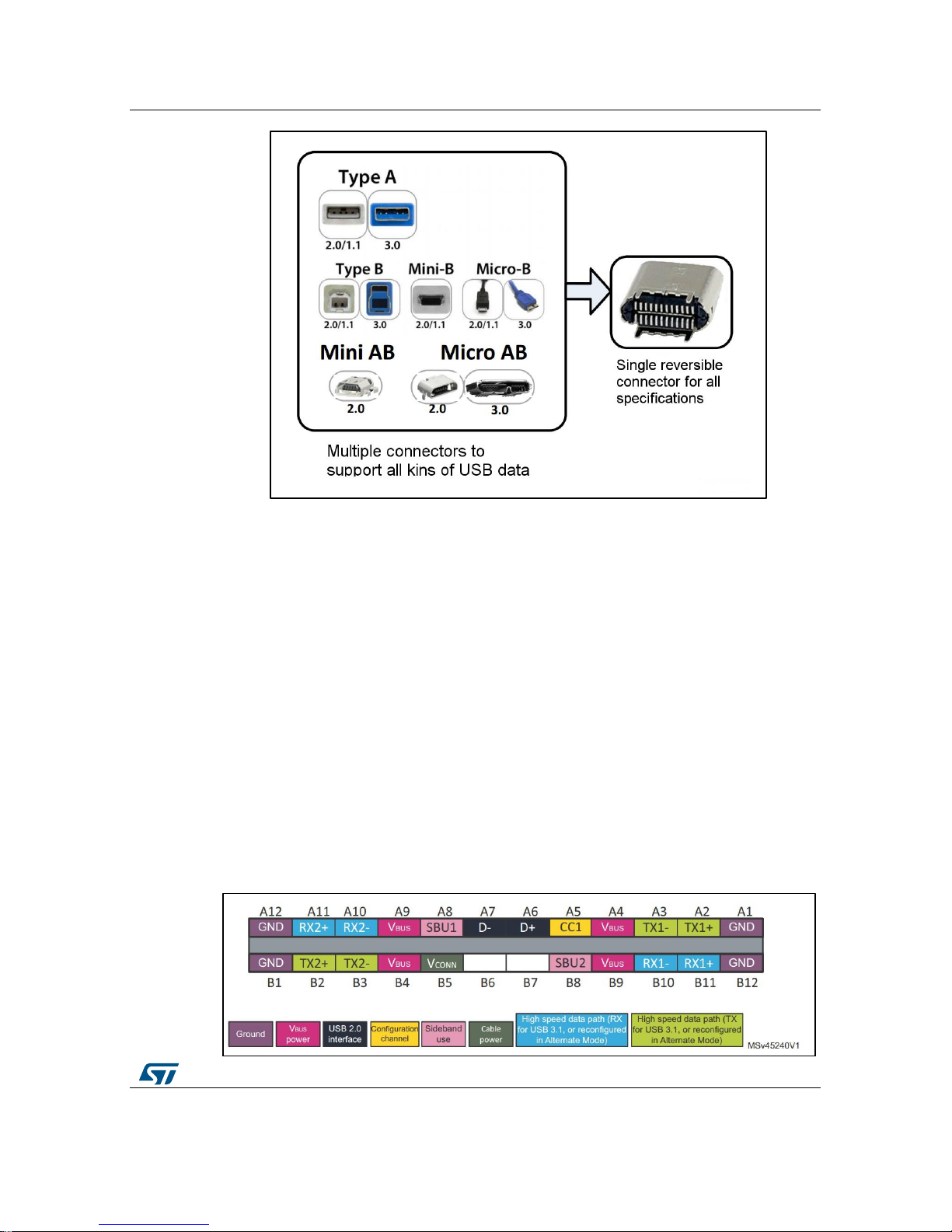
Figure 2: USB plug form factors .................................................................................................................7
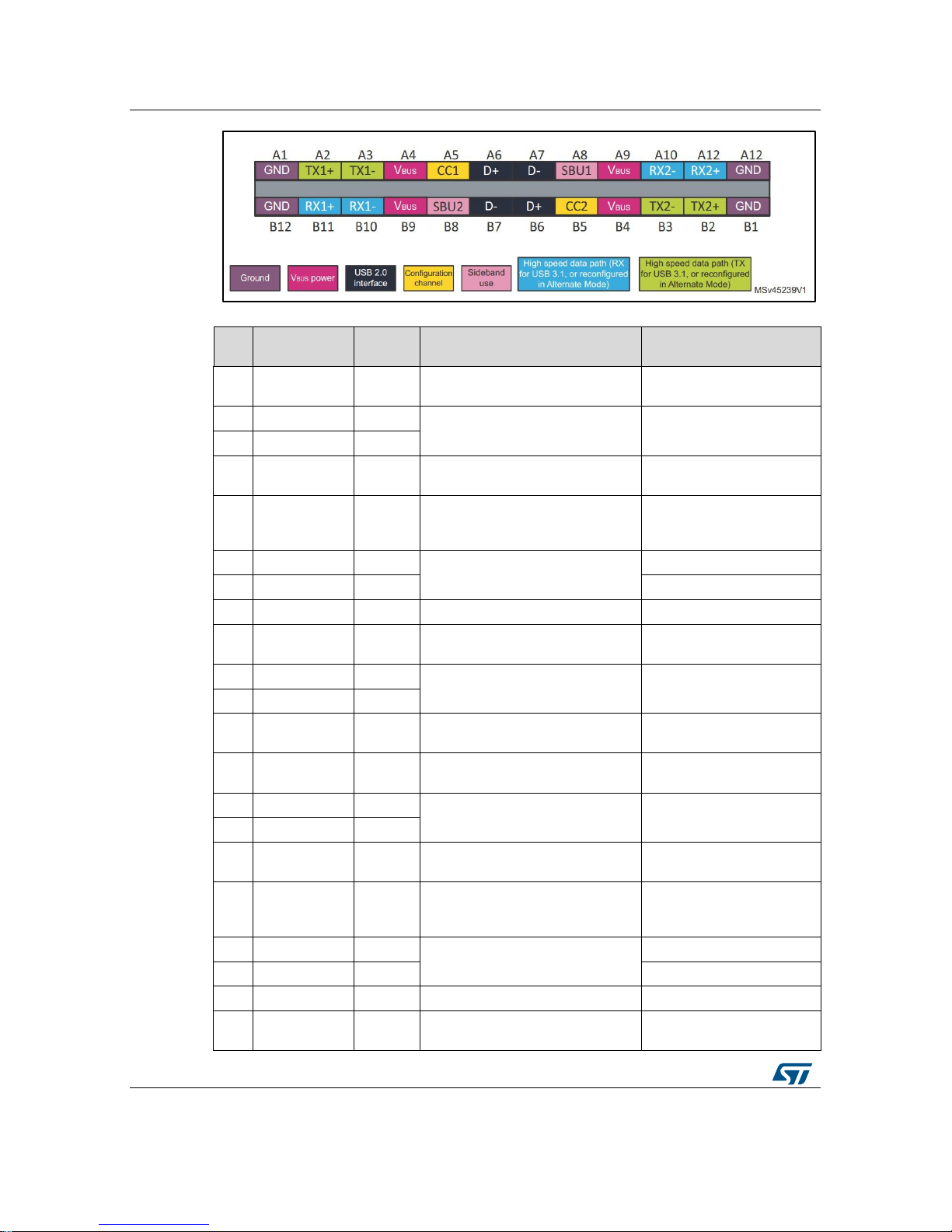
Figure 3: USB Type-C plug pinout..............................................................................................................7
Figure 4: USB Type-C receptacle pinout....................................................................................................8
Figure 5: USB power delivery architecture...............................................................................................10
Figure 6: Pull up/down CC detection ........................................................................................................12
Figure 7: Message flow during power negotiation....................................................................................14
Figure 8: Pins available for reconfiguration on the plug of the full-featured cable ...................................15
Figure 9: Pins available for reconfiguration on the receptacle for direct connect applications.................15
Figure 10: The two boards composing the P-NUCLEO-USB002 kit ........................................................17
Figure 11: Block scheme of the complete architecture.............................................................................19
Figure 12: STM32 Nucleo development board.........................................................................................20
Figure 13: STM32 Nucleo board top and bottom view .............................................................................21
Figure 14: P-NUCLEO-USB002 expansion board....................................................................................22
Figure 15: P-NUCLEO-USB002 expansion board functional blocks........................................................22
Figure 16: P-NUCLEO-USB002 expansion board connectors and jumpers............................................23
Figure 17: P-NUCLEO-USB002 expansion board silkscreen...................................................................23
Figure 18: P-NUCLEO-USB002 expansion board USB Type-C receptacle and current sensing (port 0)
schematic view..........................................................................................................................................24
Figure 19: P-NUCLEO-USB002 expansion board USB Type-C receptacle and Current sensing (port 1)
schematic view..........................................................................................................................................25
Figure 20: P-NUCLEO-USB002 expansion board Port 0 Current sensing stage schematic view...........25
Figure 21: P-NUCLEO-USB002 expansion board Port 1 Current sensing stage schematic view...........26
Figure 22: STUSB1602 front end for Port 0 .............................................................................................27
Figure 23: P-NUCLEO-USB002 expansion board: JP000 and JP001 jumper settings to provide VCONN
through the local voltage regulator ...........................................................................................................29
Figure 24: P-NUCLEO-USB002 expansion board Port 0 schematic view of the VBUS management
mechanism................................................................................................................................................30
Figure 25: P-NUCLEO-USB002 expansion board Port 1 schematic view of the VBUS management
mechanism................................................................................................................................................30
Figure 26: P-NUCLEO-USB002 expansion board: schematic view of the load switches of the local
power management..................................................................................................................................31
Figure 27: P-NUCLEO-USB002 expansion board: schematic view of the local DC-DC converter..........32
Figure 28: P-NUCLEO-USB002 expansion board: STSAFE-A100 schematic view ................................32
Figure 29: P-NUCLEO-USB002 expansion board: JP100 and JP101 connectors for USB 2.0
configurations............................................................................................................................................34
Figure 30: P-NUCLEO-USB002: CN13 and C14 connector pinout..........................................................35
Figure 31: P-NUCLEO-USB002: CN4 connector .....................................................................................36
Figure 32: P-NUCLEO-USB002 expansion board CN2_1 and CN3_TX pin indications .........................37
Figure 33: P-NUCLEO-USB002 mounting orientation..............................................................................39
Figure 34: P-NUCLEO-USB002 expansion board circuit schematic - global view...................................43
Figure 35: P-NUCLEO-USB002 expansion board circuit schematic - MCU interface .............................43
Figure 36: P-NUCLEO-USB002 expansion board circuit schematic - STUSB1602 front end Port0 .......44
Figure 37: P-NUCLEO-USB002 expansion board circuit schematic - STUSB1602 front end Port1 .......44
Figure 38: P-NUCLEO-USB002 expansion board circuit schematic - local power ..................................45
Figure 39: P-NUCLEO-USB002 expansion board circuit schematic - local voltage supply.....................45
Figure 40: P-NUCLEO-USB002 expansion board circuit schematic - Type-C Connector 0....................46
Figure 41: P-NUCLEO-USB002 expansion board circuit schematic - Type-C Connector 1....................46
Figure 42: P-NUCLEO-USB002 expansion board circuit schematic - Current Sensing C0.....................47
Figure 43: P-NUCLEO-USB002 expansion board circuit schematic - Current Sensing C1.....................47
Figure 44: P-NUCLEO-USB002 expansion board circuit schematic - security........................................47